EP0778518B1 - Verfahren zum Erzeugen eines Parameters J0 bezüglich der Verwendung von modularen Operationen nach der Montgomery-Methode - Google Patents
Verfahren zum Erzeugen eines Parameters J0 bezüglich der Verwendung von modularen Operationen nach der Montgomery-Methode Download PDFInfo
- Publication number
- EP0778518B1 EP0778518B1 EP96470022A EP96470022A EP0778518B1 EP 0778518 B1 EP0778518 B1 EP 0778518B1 EP 96470022 A EP96470022 A EP 96470022A EP 96470022 A EP96470022 A EP 96470022A EP 0778518 B1 EP0778518 B1 EP 0778518B1
- Authority
- EP
- European Patent Office
- Prior art keywords
- register
- bits
- bit
- significant bit
- content
- Prior art date
- Legal status (The legal status is an assumption and is not a legal conclusion. Google has not performed a legal analysis and makes no representation as to the accuracy of the status listed.)
- Expired - Lifetime
Links
Images

Classifications
-
- G—PHYSICS
- G06—COMPUTING OR CALCULATING; COUNTING
- G06F—ELECTRIC DIGITAL DATA PROCESSING
- G06F7/00—Methods or arrangements for processing data by operating upon the order or content of the data handled
- G06F7/60—Methods or arrangements for performing computations using a digital non-denominational number representation, i.e. number representation without radix; Computing devices using combinations of denominational and non-denominational quantity representations, e.g. using difunction pulse trains, STEELE computers, phase computers
- G06F7/72—Methods or arrangements for performing computations using a digital non-denominational number representation, i.e. number representation without radix; Computing devices using combinations of denominational and non-denominational quantity representations, e.g. using difunction pulse trains, STEELE computers, phase computers using residue arithmetic
- G06F7/728—Methods or arrangements for performing computations using a digital non-denominational number representation, i.e. number representation without radix; Computing devices using combinations of denominational and non-denominational quantity representations, e.g. using difunction pulse trains, STEELE computers, phase computers using residue arithmetic using Montgomery reduction
Definitions
- the invention relates to a method for producing a calculation parameter involved in the implementation of modular operations according to the Montgomery method.
- Modular operations according to the Montgomery method make it possible to perform modular calculations in a finite body GF (2 n ) (Welsh body of 2 n elements) without performing division.
- the montgomery method allows the calculation of the basic operation, called P fieid .
- n is equal to 256, 512, and in the very near future 1024.
- Bt 32.
- k * Bt ⁇ n> (k - 1) * Bt there exists an integer k such that k * Bt ⁇ n> (k - 1) * Bt.
- EP-A-0 502 782 discloses circuits dedicated to modular calculations.
- EP-A-0 502 782 discloses, among other things, a parallel architecture calculation circuit dedicated to the calculation of the parameter J 0 associated with the Montgomery method.
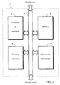
- FIG. 1 represents an encryption circuit 1 which comprises a processing processor 2, for example a microprocessor 8, 16 or 32 bits, a memory 3, a coprocessor 4, a circuit dedicated to the calculation of J 0 5 and a communication bus 6.
- the communication bus 6 links together processor 2, memory 3, coprocessor 4 and the calculation circuit of J 0 .
- This communication bus 6 also serves to receive a clear or encrypted message which, after processing, will come out, after a certain processing time, by this same communication bus 6 after being encrypted or decrypted.
- Such an encryption circuit 1 allows several processing possibilities.
- the communication bus 6 includes all the signals which are exchanged inside the encryption circuit 1.
- a first possibility of treatment is purely software.
- the processing processor 2 will perform all the encryption or decryption calculations using a program stored in the memory 3. Such processing does not require the presence of the coprocessor 4 and the calculation circuit of J 0 5 but takes considerable processing time.
- a second processing possibility consists in having all the calculations processed by the coprocessor 4, the processor 2 only serving to control the good progress of the operations. This possibility is very fast but limits the encryption to operations using data compatible with coprocessor 4 and therefore prevents certain calculations from being made.
- the use of a circuit for calculating J 0 5 makes it possible to optimize the specific calculation of the parameter J 0 .
- a third processing possibility consists in a mixed use of processor 2, coprocessor 4 and the calculation circuit of J 0 . This makes it possible to process all types of encryption with a duration less than the first purely software possibility.
- Figure 2 shows coprocessor 4 modular arithmetic.
- J 0 is calculated externally to the coprocessor.
- the invention proposes a circuit 5 dedicated inter alia to the calculation of J 0 .
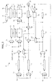
- a preferred embodiment of this circuit 5 is visible in Figure 3 and it includes among others: a first, a second and a third shift register 40, 41 and 42 Bt bits each having a serial input and an output series, three multiplexers 43, 44 and 45 each having a first and second entry and exit, one adder 46 having first and second input serial and a serial output and a test circuit 47 having an entry and an exit.
- the first register 40 has its input connected to the output of the multiplexer 43
- the first register 40 has its output connected to the first input of adder 46
- the second register 41 has its input connected to the output of test circuit 47
- the second register has its output connected to an output terminal
- the third register has its input connected to the output of multiplexer 44
- the third register has its output linked on the one hand to the first input of multiplexer 44 and secondly to the first input of multiplexer 45
- multiplexer 43 has its first input linked on the one hand to the output of the adder 46 and on the other hand at the input of the circuit 47
- multiplexer 43 has its second input connected to a first input terminal
- the multiplexer 44 has its second input connected to a second terminal input
- multiplexer 45 has its second input connected to a logic zero (usually 0V).
- control signals of the multiplexers and of the registers are not shown in order to clarify the diagram in FIG. 3.
- the different control signals are generated by a state machine easily achievable by those skilled in the art after having read the development of the production process for parameter J 0 using this circuit.
- the second register 41 can coincide with the register 17, this makes it possible to delete Bt cycles d 'clock and obtain the parameter J 0 in BT 2 + (2 * Bt) - 1 clock cycles.
- the second register 41 can coincide with the register 17, this allows delete Bt clock cycles and obtain the parameter J 0 in BT 2 + (3 * Bt) clock cycles.
- This second method is slightly slower than the first method stated, it is however noted that for this method, the steps E1 and E2 can be combined, which again makes it possible to save Bt clock cycles.
- step E4 In total, counting E4, we use between 4 * Bt - 2 and Bt 2 + (2 * Bt) - 1 clock cycles.
- the Bt clock cycles used in step E4 may or may not be subtracted.
- counting E4 we use between 4 * Bt and Bt 2 + (3 * Bt) clock cycles.
- the Bt clock cycles used in step E4 may or may not be subtracted.
- N 0 can appear as a calculation step which would not be counted. It is quite possible to carry out this calculation in "soft" in the processing processor 2 while carrying out the loading of the data N 0 and N 0 + 1. If the processing processor is not very efficient and does not allow these simultaneous treatments , it is then possible for a person skilled in the art to add an additional serial adder between an input terminal and the multiplexer 43, the addition being carried out simultaneously with the loading without adding additional delays.
- FIG. 4 shows a register 40, which could be register 41 or 42 which is broken down into two 50 and 51 shift sub-registers of Bt bits each having a serial input and output, a multiplexer 52 having a first input connected to the output from register 50, a second input connected to the input of register 50 and an output connected to the input of register 51.
- a register 40 which could be register 41 or 42 which is broken down into two 50 and 51 shift sub-registers of Bt bits each having a serial input and output, a multiplexer 52 having a first input connected to the output from register 50, a second input connected to the input of register 50 and an output connected to the input of register 51.
- Such a device behaves like a shift register 40 having its input confused with the entry of register 50 and its exit confused with the exit from register 51.
- the shift register 40 will have a size varying from Bt or 2 * Bt bits.
- a second possibility is to use a maximum of elements of the coprocessor 4.
- the subtraction circuit 27 must be replaced by a circuit capable of performing as well additions as subtractions to have the functionality of the adder 46.
- register 17 must be substituted for the second register 41.
- test circuit 47 In order to be able to carry out the functionality of the calculation of J 0 , only one test circuit 47 is missing which will have its output connected to the input of register 17 and its input connected to one of the bits of register 10, there is also missing a connection between the output of the addition / subtraction circuit which replaces the subtraction circuit 27 and a fourth input of the multiplexer 13.
Landscapes
- Physics & Mathematics (AREA)
- Engineering & Computer Science (AREA)
- General Physics & Mathematics (AREA)
- Mathematical Analysis (AREA)
- Mathematical Optimization (AREA)
- Pure & Applied Mathematics (AREA)
- Computational Mathematics (AREA)
- Theoretical Computer Science (AREA)
- Computing Systems (AREA)
- Mathematical Physics (AREA)
- General Engineering & Computer Science (AREA)
- Error Detection And Correction (AREA)
- Complex Calculations (AREA)
- Logic Circuits (AREA)
Claims (7)
- Verfahren zur Erzeugung eines Parameters J0 in einem Koprozessor mit modularer Arithmetik einer integrierten Schaltung zur Durchführung einer modularen Operation nach der Montgomery-Methode, wobei der Koprozessor Schieberegister mit Bt und k * Bt Bits (10 bis 12, 16 bis 18), serielle Additions- und Subtraktionsschaltungen (27 bis 31), eine Testschaltung (35) und weitere Einrichtungen zum Ausführen modularer Operationen nach der Montgomery-Methode umfaßt,
dadurch gekennzeichnet, daß
J0 auf Bt Bits codiert ist und somit
((J0 * N0) + 1) mod 2 Bt = 0 gilt, wobei N0 eine auf Bt Bits codierte Information ist, und daß folgende Schritte ausgeführt werden:E1: Laden der Information N0 in ein erstes und ein drittes Register (40 und 42) mit Bt Bits, wobei das Bit von N0 mit geringem Gewicht gleich 1 ist,E2: Laden einer 1 auf das Bit mit großem Gewicht eines zweiten Registers (41) mit Bt Bits,E3: Ausführen einer mit dem Index i bezeichneten Schleife, mit i zwischen 1 und Bt - 1, wobei jede Iteration die folgenden Schritte aufweist:B1: Der Inhalt des ersten Registers (40) wird um eine Einheit nach rechts verschoben,B2: das Bit mit dem geringsten Gewicht des ersten Registers (40) wird getestet:T1: ist das getestete Bit gleich 1, wird der Inhalt des zweiten Registers (41) um eine Einheit nach rechts verschoben und eine 0 in das Bit mit großem Gewicht geladen,T2: ist das getestete Bit gleich 0, wird der Inhalt des zweiten Registers (41) um eine Einheit nach rechts verschoben und eine 1 in das Bit mit großem Gewicht geladen, der Inhalt des ersten und des dritten Registers (40 und 42) werden in einem Addierer (46) bitweise addiert, wobei ein Ausgang des Addierers (46) an einen Eingang des ersten Registers (40) angeschlossen ist und ein Eingang des dritten Registers (42) mit seinem Eingang zur Schleife geschaltet ist,E4: das zweite Register (41) enthält den gewünschten Parameter J0. - Verfahren zur Erzeugung eines Parameters J0 in einem Koprozessor mit modularer Arithmetik einer integrierten Schaltung zur Durchführung einer modularen Operation nach der Montgomery-Methode,
dadurch gekennzeichnet, daß
J0 auf Bt Bits codiert ist und somit
((J0 * N0) + 1) mod 2 Bt = 0 gilt, wobei N0 eine auf Bt Bits codierte Information ist, und daß folgende Schritte ausgeführt werden:E1: Laden der Information N0 in ein erstes und ein drittes Register (40 und 42) mit Bt Bits, wobei das Bit mit geringem Gewicht von N0 gleich 1 ist,E2: Laden einer 1 auf das Bit mit großem Gewicht eines zweiten Registers (41) mit Bt Bits,E3: Ausführen einer mit dem Index i bezeichneten Schleife, mit i zwischen 1 und Bt - 1, wobei jede Iteration die folgenden Schritte aufweist:B1: nach der Durchführung des Tests beim Schritt 32 wird der Inhalt des ersten Registers (40) um eine Einheit nach rechts verschoben,B2: das zweite Bit mit dem geringsten Gewicht des ersten Registers (40) wird getestet:T1: ist das getestete Bit gleich 1, wird der Inhalt des zweiten Registers (41) um eine Einheit nach rechts verschoben, und eine 0 wird in das Bit mit großem Gewicht des zweiten Registers geladen,T2: ist das getestete Bit gleich 0, wird der Inhalt des zweiten Registers (41) um eine Einheit nach rechts verschoben, und eine 1 wird in das Bit mit großem Gewicht geladen, der Inhalt des ersten und des dritten Registers (40 und 42) wird in einem Addierer (46) bitweise addiert, wobei ein Ausgang des Addierers (46) an einen Eingang des ersten Registers (40) angeschlossen ist und wobei ein Ausgang des dritten Registers (42) mit seinem Eingang zur Schleife geschaltet ist,E4: das dritte Register (41) enthält den gewünschten Parameter J0. - Verfahren nach Anspruch 2, dadurch gekennzeichnet, daß der während des Schrittes B2 durchgeführte Test mit dem Bit mit der Wertigkeit 21 der dem Test voranstehenden Addition durchgeführt wird.
- Verfahren nach einem der Ansprüche 1 bis 3, dadurch gekennzeichnet, daß in einer ersten Alternative T1 des Testes darüber hinaus im Addierer (46) eine bitweise Addition des Inhalts des ersten Registers (40) mit einer Null durchgeführt wird, wobei der Ausgang des Addierers (46) mit dem Eingang des ersten Registers (40) verbunden ist.
- Verfahren nach Anspruch 4, dadurch gekennzeichnet, daß der Schritt der folgende ist:E2: der Inhalt des zweiten Registers (41) wird um eine Einheit nach rechts verschoben, eine 1 wird auf das Bit mit großem Gewicht geladen, der Inhalt des ersten Registers (40) wird bitweise im Addierer (46) zu einer Null addiert, wobei der Ausgang des Addierers (46) mit dem Eingang des ersten Registers (40) verbunden ist.
- Verfahren nach einem der Ansprüche 1 bis 5, dadurch gekennzeichnet, daß die ersten, zweiten und dritten Register (40, 41, 42) mehrere Multiplexer (52, 54) aufweisen, die eine variable Größe haben können.
- Verfahren nach Anspruch 6, dadurch gekennzeichnet, daß die Größe des ersten und des dritten Registers (40 und 42) während der Erzeugung des Parameters J0 abnimmt.
Applications Claiming Priority (2)
| Application Number | Priority Date | Filing Date | Title |
|---|---|---|---|
| FR9514614 | 1995-12-04 | ||
| FR9514614A FR2741973B1 (fr) | 1995-12-04 | 1995-12-04 | Procede de production d'un parametre jo associe a la mise en oeuvre d'operation modulaire selon la methode de montgomery |
Publications (2)
| Publication Number | Publication Date |
|---|---|
| EP0778518A1 EP0778518A1 (de) | 1997-06-11 |
| EP0778518B1 true EP0778518B1 (de) | 2000-01-19 |
Family
ID=9485344
Family Applications (1)
| Application Number | Title | Priority Date | Filing Date |
|---|---|---|---|
| EP96470022A Expired - Lifetime EP0778518B1 (de) | 1995-12-04 | 1996-11-27 | Verfahren zum Erzeugen eines Parameters J0 bezüglich der Verwendung von modularen Operationen nach der Montgomery-Methode |
Country Status (4)
| Country | Link |
|---|---|
| US (1) | US5999953A (de) |
| EP (1) | EP0778518B1 (de) |
| DE (1) | DE69606273T2 (de) |
| FR (1) | FR2741973B1 (de) |
Families Citing this family (6)
| Publication number | Priority date | Publication date | Assignee | Title |
|---|---|---|---|---|
| FR2743646B1 (fr) * | 1996-01-12 | 1998-03-06 | Sgs Thomson Microelectronics | Coprocesseur d'arithmetique modulaire comportant un circuit de division entiere |
| FR2768245B1 (fr) * | 1997-09-09 | 1999-10-15 | Sgs Thomson Microelectronics | Procede de production d'une division entiere avec un coprocesseur d'arithmetique modulaire |
| FR2773231B1 (fr) * | 1997-12-31 | 2000-02-25 | Sgs Thomson Microelectronics | Procede de production ameliore d'un parametre jo associe a la mise en oeuvre d'operations modulaires selon la methode de montgomery |
| FR2775369B1 (fr) * | 1998-02-26 | 2001-08-03 | Sgs Thomson Microelectronics | Procede de mise en oeuvre d'une multiplication modulaire specifique relative a la methode de montgomery |
| US7085791B2 (en) * | 2003-02-14 | 2006-08-01 | Lucent Technologies Inc. | Method and apparatus for generating a pseudo random number |
| US8526601B2 (en) * | 2004-04-05 | 2013-09-03 | Advanced Micro Devices, Inc. | Method of improving operational speed of encryption engine |
Family Cites Families (8)
| Publication number | Priority date | Publication date | Assignee | Title |
|---|---|---|---|---|
| US4538237A (en) * | 1983-01-18 | 1985-08-27 | Honeywell Information Systems Inc. | Method and apparatus for calculating the residue of a binary number |
| US4891781A (en) * | 1987-03-04 | 1990-01-02 | Cylink Corporation | Modulo arithmetic processor chip |
| IL97413A (en) * | 1991-03-04 | 1995-06-29 | Fortress U & T 2000 Ltd | Microcircuit for the implementation of rsa algorithm and ordinary and modular arithmetic in particular exponentiation with large operands |
| FR2679054A1 (fr) | 1991-07-10 | 1993-01-15 | Fortress U T 2000 Ltd | Procede et appareil d'exponentiation sur gf(2n). |
| US5513133A (en) * | 1992-11-30 | 1996-04-30 | Fortress U&T Ltd. | Compact microelectronic device for performing modular multiplication and exponentiation over large numbers |
| US5535225A (en) * | 1993-10-12 | 1996-07-09 | Hughes Aircraft Company | Time domain algebraic encoder/decoder |
| FR2726668B1 (fr) * | 1994-11-08 | 1997-01-10 | Sgs Thomson Microelectronics | Procede de mise en oeuvre de reduction modulaire selon la methode de montgomery |
| FR2726667B1 (fr) * | 1994-11-08 | 1997-01-17 | Sgs Thomson Microelectronics | Procede de mise en oeuvre de multiplication modulaire selon la methode montgomery |
-
1995
- 1995-12-04 FR FR9514614A patent/FR2741973B1/fr not_active Expired - Fee Related
-
1996
- 1996-11-27 EP EP96470022A patent/EP0778518B1/de not_active Expired - Lifetime
- 1996-11-27 DE DE69606273T patent/DE69606273T2/de not_active Expired - Lifetime
- 1996-12-03 US US08/759,892 patent/US5999953A/en not_active Expired - Fee Related
Also Published As
| Publication number | Publication date |
|---|---|
| FR2741973A1 (fr) | 1997-06-06 |
| FR2741973B1 (fr) | 1998-01-02 |
| DE69606273T2 (de) | 2000-05-31 |
| EP0778518A1 (de) | 1997-06-11 |
| US5999953A (en) | 1999-12-07 |
| DE69606273D1 (de) | 2000-02-24 |
Similar Documents
| Publication | Publication Date | Title |
|---|---|---|
| EP0712071B1 (de) | Verfahren zur Verwendung der modularen Multiplikation nach der Montgomery-Methode | |
| EP0712072B1 (de) | Verfahren zur Ausführung von modularen Reduktion nach der Montgomery-Methode | |
| EP0853275B1 (de) | Koprozessor mit zwei parallel arbeitenden Multiplizierschaltungen | |
| FR2867579A1 (fr) | Multiplieur modulaire de montgomery | |
| FR2822260A1 (fr) | Procedes et dispositifs pour accelerer le temps de calcul d'un produit de montgomery d'un multiplication et d'une exponentiation modulaire | |
| EP0703528B1 (de) | Elektronische Schaltung zur Modularberechnung in einem endlichen Körper | |
| EP0939362B1 (de) | Koprozessor für moduläre Arithmetik mit einer schnellen Ausführung von nicht-modulären Operationen | |
| EP0793165B1 (de) | Koprozessor für moduläre Arithmetik mit einer schnellen Ausführung von nicht-modulären Operationen | |
| FR2868628A1 (fr) | Generateur de nombres aleatoires et procede de production de nombres aleatoires | |
| EP0712070A1 (de) | Verfahren zum Erzeugen eines Fehlerkorrekturparameters in Verbindung mit der Verwendung von modularen Operationen nach der Montgomery-Methode | |
| EP0939363B1 (de) | Verfahren zur Ausführung der modularen Multiplikation nach der Montgomery-Methode | |
| EP0778518A1 (de) | Verfahren zum Erzeugen eines Parameters J0 bezüglich der Verwendung von modularen Operationen nach der Montgomery-Methode | |
| EP1071008B1 (de) | Verfahren zur Durchführung einer Multiplikation mit Akkumulation in einem Galois-Feld | |
| EP0690584B1 (de) | Schaltung zur Ortung von Fehlern in einem Reed-Solomon Dekoder | |
| EP0927928B1 (de) | Verbessertes Verfahren zum Erzeugen eines Parameters J0 bezüglich der Verwendung von modularen Operationen nach der Montgomery-Methode | |
| EP0785502B1 (de) | Verfahren zum Erzeugen eines Fehlerkorrekturparameters bezüglich der Verwendung von modularen Operationen nach der Montgomery-Methode | |
| EP1012703B1 (de) | Modulo-arithmetischer koprozessor mit einer schaltung für die division ganzer zahlen | |
| EP0947913B1 (de) | Verbessertes Verfahren zur Ausführung ganzzahliger Division | |
| EP0784262B1 (de) | Einrichtung und Verfahren zur Verbesserung der Verarbeitungsgeschwindigkeit eines Koprozessors für moduläre Arithmetik | |
| FR2818765A1 (fr) | Multiplicateur modulaire et processeur de cryptage/decryptage utilisant le multiplicateur modulaire | |
| EP0902359B1 (de) | Verfahren und Anordnung zur Durchführung ganzzahliger Divisionsoperationen mit einem modulo-arithmetischen Koprozessor | |
| FR2771525A1 (fr) | Procede de production d'un parametre de correction d'erreur associe a la mise en oeuvre d'operation modulaire selon la methode de montgomery | |
| WO2005024627A2 (fr) | Reduction modulaire pour un procede cryptographique, et coprocesseur pour la realisation d’une telle reduction modulaire | |
| FR2788616A1 (fr) | Circuit de multiplication dans un corps de galois | |
| FR2745646A1 (fr) | Coprocesseur d'arithmetique modulaire permettant de realiser des operations non modulaires rapidement |
Legal Events
| Date | Code | Title | Description |
|---|---|---|---|
| PUAI | Public reference made under article 153(3) epc to a published international application that has entered the european phase |
Free format text: ORIGINAL CODE: 0009012 |
|
| AK | Designated contracting states |
Kind code of ref document: A1 Designated state(s): DE FR GB IT |
|
| 17P | Request for examination filed |
Effective date: 19970730 |
|
| 17Q | First examination report despatched |
Effective date: 19970916 |
|
| RAP3 | Party data changed (applicant data changed or rights of an application transferred) |
Owner name: STMICROELECTRONICS S.A. |
|
| GRAG | Despatch of communication of intention to grant |
Free format text: ORIGINAL CODE: EPIDOS AGRA |
|
| GRAG | Despatch of communication of intention to grant |
Free format text: ORIGINAL CODE: EPIDOS AGRA |
|
| GRAH | Despatch of communication of intention to grant a patent |
Free format text: ORIGINAL CODE: EPIDOS IGRA |
|
| GRAH | Despatch of communication of intention to grant a patent |
Free format text: ORIGINAL CODE: EPIDOS IGRA |
|
| GRAA | (expected) grant |
Free format text: ORIGINAL CODE: 0009210 |
|
| AK | Designated contracting states |
Kind code of ref document: B1 Designated state(s): DE FR GB IT |
|
| GBT | Gb: translation of ep patent filed (gb section 77(6)(a)/1977) |
Effective date: 20000119 |
|
| REF | Corresponds to: |
Ref document number: 69606273 Country of ref document: DE Date of ref document: 20000224 |
|
| ITF | It: translation for a ep patent filed | ||
| PLBE | No opposition filed within time limit |
Free format text: ORIGINAL CODE: 0009261 |
|
| STAA | Information on the status of an ep patent application or granted ep patent |
Free format text: STATUS: NO OPPOSITION FILED WITHIN TIME LIMIT |
|
| 26N | No opposition filed | ||
| REG | Reference to a national code |
Ref country code: GB Ref legal event code: IF02 |
|
| PGFP | Annual fee paid to national office [announced via postgrant information from national office to epo] |
Ref country code: GB Payment date: 20031126 Year of fee payment: 8 |
|
| PG25 | Lapsed in a contracting state [announced via postgrant information from national office to epo] |
Ref country code: GB Free format text: LAPSE BECAUSE OF NON-PAYMENT OF DUE FEES Effective date: 20041127 |
|
| GBPC | Gb: european patent ceased through non-payment of renewal fee |
Effective date: 20041127 |
|
| PG25 | Lapsed in a contracting state [announced via postgrant information from national office to epo] |
Ref country code: IT Free format text: LAPSE BECAUSE OF NON-PAYMENT OF DUE FEES;WARNING: LAPSES OF ITALIAN PATENTS WITH EFFECTIVE DATE BEFORE 2007 MAY HAVE OCCURRED AT ANY TIME BEFORE 2007. THE CORRECT EFFECTIVE DATE MAY BE DIFFERENT FROM THE ONE RECORDED. Effective date: 20051127 |
|
| PGFP | Annual fee paid to national office [announced via postgrant information from national office to epo] |
Ref country code: FR Payment date: 20071129 Year of fee payment: 12 |
|
| REG | Reference to a national code |
Ref country code: FR Ref legal event code: ST Effective date: 20090731 |
|
| PGFP | Annual fee paid to national office [announced via postgrant information from national office to epo] |
Ref country code: DE Payment date: 20101025 Year of fee payment: 15 |
|
| PG25 | Lapsed in a contracting state [announced via postgrant information from national office to epo] |
Ref country code: FR Free format text: LAPSE BECAUSE OF NON-PAYMENT OF DUE FEES Effective date: 20081130 |
|
| REG | Reference to a national code |
Ref country code: DE Ref legal event code: R119 Ref document number: 69606273 Country of ref document: DE Effective date: 20120601 |
|
| PG25 | Lapsed in a contracting state [announced via postgrant information from national office to epo] |
Ref country code: DE Free format text: LAPSE BECAUSE OF NON-PAYMENT OF DUE FEES Effective date: 20120601 |