EP0145557A2 - Procédé de brasage à la vague et capteur capillaire de brasure mettant en oeuvre ce procédé - Google Patents
Procédé de brasage à la vague et capteur capillaire de brasure mettant en oeuvre ce procédé Download PDFInfo
- Publication number
- EP0145557A2 EP0145557A2 EP84402304A EP84402304A EP0145557A2 EP 0145557 A2 EP0145557 A2 EP 0145557A2 EP 84402304 A EP84402304 A EP 84402304A EP 84402304 A EP84402304 A EP 84402304A EP 0145557 A2 EP0145557 A2 EP 0145557A2
- Authority
- EP
- European Patent Office
- Prior art keywords
- component
- substrate
- capillary
- solder
- connection pads
- Prior art date
- Legal status (The legal status is an assumption and is not a legal conclusion. Google has not performed a legal analysis and makes no representation as to the accuracy of the status listed.)
- Granted
Links
Images


Classifications
-
- B—PERFORMING OPERATIONS; TRANSPORTING
- B23—MACHINE TOOLS; METAL-WORKING NOT OTHERWISE PROVIDED FOR
- B23K—SOLDERING OR UNSOLDERING; WELDING; CLADDING OR PLATING BY SOLDERING OR WELDING; CUTTING BY APPLYING HEAT LOCALLY, e.g. FLAME CUTTING; WORKING BY LASER BEAM
- B23K1/00—Soldering, e.g. brazing, or unsoldering
- B23K1/20—Preliminary treatment of work or areas to be soldered, e.g. in respect of a galvanic coating
-
- H—ELECTRICITY
- H05—ELECTRIC TECHNIQUES NOT OTHERWISE PROVIDED FOR
- H05K—PRINTED CIRCUITS; CASINGS OR CONSTRUCTIONAL DETAILS OF ELECTRIC APPARATUS; MANUFACTURE OF ASSEMBLAGES OF ELECTRICAL COMPONENTS
- H05K3/00—Apparatus or processes for manufacturing printed circuits
- H05K3/30—Assembling printed circuits with electric components, e.g. with resistors
- H05K3/32—Assembling printed circuits with electric components, e.g. with resistors electrically connecting electric components or wires to printed circuits
- H05K3/34—Assembling printed circuits with electric components, e.g. with resistors electrically connecting electric components or wires to printed circuits by soldering
- H05K3/341—Surface mounted components
- H05K3/3421—Leaded components
- H05K3/3426—Leaded components characterised by the leads
-
- H—ELECTRICITY
- H05—ELECTRIC TECHNIQUES NOT OTHERWISE PROVIDED FOR
- H05K—PRINTED CIRCUITS; CASINGS OR CONSTRUCTIONAL DETAILS OF ELECTRIC APPARATUS; MANUFACTURE OF ASSEMBLAGES OF ELECTRICAL COMPONENTS
- H05K3/00—Apparatus or processes for manufacturing printed circuits
- H05K3/30—Assembling printed circuits with electric components, e.g. with resistors
- H05K3/32—Assembling printed circuits with electric components, e.g. with resistors electrically connecting electric components or wires to printed circuits
- H05K3/34—Assembling printed circuits with electric components, e.g. with resistors electrically connecting electric components or wires to printed circuits by soldering
- H05K3/341—Surface mounted components
- H05K3/3431—Leadless components
- H05K3/3442—Leadless components having edge contacts, e.g. leadless chip capacitors, chip carriers
-
- H—ELECTRICITY
- H05—ELECTRIC TECHNIQUES NOT OTHERWISE PROVIDED FOR
- H05K—PRINTED CIRCUITS; CASINGS OR CONSTRUCTIONAL DETAILS OF ELECTRIC APPARATUS; MANUFACTURE OF ASSEMBLAGES OF ELECTRICAL COMPONENTS
- H05K3/00—Apparatus or processes for manufacturing printed circuits
- H05K3/30—Assembling printed circuits with electric components, e.g. with resistors
- H05K3/32—Assembling printed circuits with electric components, e.g. with resistors electrically connecting electric components or wires to printed circuits
- H05K3/34—Assembling printed circuits with electric components, e.g. with resistors electrically connecting electric components or wires to printed circuits by soldering
- H05K3/3465—Application of solder
- H05K3/3468—Application of molten solder, e.g. dip soldering
-
- B—PERFORMING OPERATIONS; TRANSPORTING
- B23—MACHINE TOOLS; METAL-WORKING NOT OTHERWISE PROVIDED FOR
- B23K—SOLDERING OR UNSOLDERING; WELDING; CLADDING OR PLATING BY SOLDERING OR WELDING; CUTTING BY APPLYING HEAT LOCALLY, e.g. FLAME CUTTING; WORKING BY LASER BEAM
- B23K2101/00—Articles made by soldering, welding or cutting
- B23K2101/36—Electric or electronic devices
- B23K2101/40—Semiconductor devices
-
- H—ELECTRICITY
- H05—ELECTRIC TECHNIQUES NOT OTHERWISE PROVIDED FOR
- H05K—PRINTED CIRCUITS; CASINGS OR CONSTRUCTIONAL DETAILS OF ELECTRIC APPARATUS; MANUFACTURE OF ASSEMBLAGES OF ELECTRICAL COMPONENTS
- H05K2201/00—Indexing scheme relating to printed circuits covered by H05K1/00
- H05K2201/09—Shape and layout
- H05K2201/09145—Edge details
- H05K2201/09181—Notches in edge pads
-
- H—ELECTRICITY
- H05—ELECTRIC TECHNIQUES NOT OTHERWISE PROVIDED FOR
- H05K—PRINTED CIRCUITS; CASINGS OR CONSTRUCTIONAL DETAILS OF ELECTRIC APPARATUS; MANUFACTURE OF ASSEMBLAGES OF ELECTRICAL COMPONENTS
- H05K2201/00—Indexing scheme relating to printed circuits covered by H05K1/00
- H05K2201/09—Shape and layout
- H05K2201/09209—Shape and layout details of conductors
- H05K2201/09372—Pads and lands
- H05K2201/09381—Shape of non-curved single flat metallic pad, land or exposed part thereof; Shape of electrode of leadless component
-
- H—ELECTRICITY
- H05—ELECTRIC TECHNIQUES NOT OTHERWISE PROVIDED FOR
- H05K—PRINTED CIRCUITS; CASINGS OR CONSTRUCTIONAL DETAILS OF ELECTRIC APPARATUS; MANUFACTURE OF ASSEMBLAGES OF ELECTRICAL COMPONENTS
- H05K2201/00—Indexing scheme relating to printed circuits covered by H05K1/00
- H05K2201/10—Details of components or other objects attached to or integrated in a printed circuit board
- H05K2201/10431—Details of mounted components
- H05K2201/10507—Involving several components
- H05K2201/10522—Adjacent components
-
- H—ELECTRICITY
- H05—ELECTRIC TECHNIQUES NOT OTHERWISE PROVIDED FOR
- H05K—PRINTED CIRCUITS; CASINGS OR CONSTRUCTIONAL DETAILS OF ELECTRIC APPARATUS; MANUFACTURE OF ASSEMBLAGES OF ELECTRICAL COMPONENTS
- H05K2201/00—Indexing scheme relating to printed circuits covered by H05K1/00
- H05K2201/10—Details of components or other objects attached to or integrated in a printed circuit board
- H05K2201/10613—Details of electrical connections of non-printed components, e.g. special leads
- H05K2201/10621—Components characterised by their electrical contacts
- H05K2201/10727—Leadless chip carrier [LCC], e.g. chip-modules for cards
-
- H—ELECTRICITY
- H05—ELECTRIC TECHNIQUES NOT OTHERWISE PROVIDED FOR
- H05K—PRINTED CIRCUITS; CASINGS OR CONSTRUCTIONAL DETAILS OF ELECTRIC APPARATUS; MANUFACTURE OF ASSEMBLAGES OF ELECTRICAL COMPONENTS
- H05K2201/00—Indexing scheme relating to printed circuits covered by H05K1/00
- H05K2201/10—Details of components or other objects attached to or integrated in a printed circuit board
- H05K2201/10613—Details of electrical connections of non-printed components, e.g. special leads
- H05K2201/10742—Details of leads
- H05K2201/10886—Other details
- H05K2201/10946—Leads attached onto leadless component after manufacturing the component
-
- H—ELECTRICITY
- H05—ELECTRIC TECHNIQUES NOT OTHERWISE PROVIDED FOR
- H05K—PRINTED CIRCUITS; CASINGS OR CONSTRUCTIONAL DETAILS OF ELECTRIC APPARATUS; MANUFACTURE OF ASSEMBLAGES OF ELECTRICAL COMPONENTS
- H05K2203/00—Indexing scheme relating to apparatus or processes for manufacturing printed circuits covered by H05K3/00
- H05K2203/04—Soldering or other types of metallurgic bonding
- H05K2203/046—Means for drawing solder, e.g. for removing excess solder from pads
-
- H—ELECTRICITY
- H05—ELECTRIC TECHNIQUES NOT OTHERWISE PROVIDED FOR
- H05K—PRINTED CIRCUITS; CASINGS OR CONSTRUCTIONAL DETAILS OF ELECTRIC APPARATUS; MANUFACTURE OF ASSEMBLAGES OF ELECTRICAL COMPONENTS
- H05K2203/00—Indexing scheme relating to apparatus or processes for manufacturing printed circuits covered by H05K3/00
- H05K2203/15—Position of the PCB during processing
- H05K2203/1581—Treating the backside of the PCB, e.g. for heating during soldering or providing a liquid coating on the backside
-
- H—ELECTRICITY
- H05—ELECTRIC TECHNIQUES NOT OTHERWISE PROVIDED FOR
- H05K—PRINTED CIRCUITS; CASINGS OR CONSTRUCTIONAL DETAILS OF ELECTRIC APPARATUS; MANUFACTURE OF ASSEMBLAGES OF ELECTRICAL COMPONENTS
- H05K3/00—Apparatus or processes for manufacturing printed circuits
- H05K3/30—Assembling printed circuits with electric components, e.g. with resistors
- H05K3/303—Assembling printed circuits with electric components, e.g. with resistors with surface mounted components
- H05K3/305—Affixing by adhesive
-
- H—ELECTRICITY
- H05—ELECTRIC TECHNIQUES NOT OTHERWISE PROVIDED FOR
- H05K—PRINTED CIRCUITS; CASINGS OR CONSTRUCTIONAL DETAILS OF ELECTRIC APPARATUS; MANUFACTURE OF ASSEMBLAGES OF ELECTRICAL COMPONENTS
- H05K3/00—Apparatus or processes for manufacturing printed circuits
- H05K3/30—Assembling printed circuits with electric components, e.g. with resistors
- H05K3/32—Assembling printed circuits with electric components, e.g. with resistors electrically connecting electric components or wires to printed circuits
- H05K3/34—Assembling printed circuits with electric components, e.g. with resistors electrically connecting electric components or wires to printed circuits by soldering
- H05K3/3405—Edge mounted components, e.g. terminals
-
- Y—GENERAL TAGGING OF NEW TECHNOLOGICAL DEVELOPMENTS; GENERAL TAGGING OF CROSS-SECTIONAL TECHNOLOGIES SPANNING OVER SEVERAL SECTIONS OF THE IPC; TECHNICAL SUBJECTS COVERED BY FORMER USPC CROSS-REFERENCE ART COLLECTIONS [XRACs] AND DIGESTS
- Y02—TECHNOLOGIES OR APPLICATIONS FOR MITIGATION OR ADAPTATION AGAINST CLIMATE CHANGE
- Y02P—CLIMATE CHANGE MITIGATION TECHNOLOGIES IN THE PRODUCTION OR PROCESSING OF GOODS
- Y02P70/00—Climate change mitigation technologies in the production process for final industrial or consumer products
- Y02P70/50—Manufacturing or production processes characterised by the final manufactured product
Definitions
- the invention relates to a wave soldering method for soldering, on a printed circuit board, components whose connection pins do not pass through the board.
- the invention also relates to capillary sensors implementing this method.
- connection of a component to a printed circuit board is made using pins belonging to the component, passing through the printed circuit board by connection holes, and by soldering the pins to pads. connection located on the opposite side of the card.
- the soldering operation is carried out by passing the card over a wave of molten solder, the face of the card carrying the connection pads coming into contact, during this passage, with the solder wave.
- the pins of the components do not pass through the printed circuit board.
- the components have connection pads which are simply brought into contact with connection pads on the printed circuit board and to which they are then soldered.
- This soldering can also be carried out by passing over a solder wave.
- the components are first placed in position on the card and immobilized, the connection pads of the components being in contact with the connection pads of the card.
- the card is then passed over the solder wave, the face carrying the connection pads as well as the components coming into contact with the solder wave.
- each component therefore bathes in the molten solder bath.
- the face of the component which attacks the solder wave is, in principle, in full contact with the solder.
- soldering The metallized parts of this face are wetted by soldering and the soldering of the connection pads of this face of the component with the pads of the card can be done.
- the card due to the temperature of the solder bath, the card must pass at a sufficient speed, to avoid the heating of the components. Therefore, the flow of the solder fluid on the sides and on the rear face of each component is such that some parts of the component may not be in contact with the solder. The soldering of the connection pads may not be ensured.
- the object of the invention is to provide a method for ensuring soldering of all the connection pads of a component on the connection pads of a substrate. It also provides a capillary solder sensor allowing this method to be implemented.
- the invention also relates to a capillary solder sensor enabling this method to be implemented.
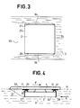
- FIG. 1 there is a printed circuit board 1 equipped with a component 2.
- a wave of molten brazing alloy 3 is produced by an alloy flow 30 channeled by two parts 31 and 32. This wave touches a plane P.
- the card 1 is placed on a transfer device, not shown and known in the art. It is moved in the direction indicated by the arrow F with its side 10 to be welded located in the P.
- Card 1 has on its face 10 not shown printed circuits and connection pads 11 and 12.
- Component 2 is bonded to face 10 of card 1 by a boss 22.
- Component 2 also has, on its face 26, connection pads such as 20 and 21 which are brought into contact (or in the vicinity) of the connection pads 11 and 12 of the card 1.
- the card 1 passes over the solder wave 3, it scans the surface of the card.
- the solder wets the metal parts with which it comes into contact and the metal parts, such as connection pads, are soldered.
- the component is immersed in the molten solder during the movement of the card. It is therefore advantageous for this displacement to be sufficiently rapid. It then turns out, due to the flow of the solder fluid around the component 2, that parts of the component are not brought into contact with the solder.
- FIG. 2 it can be seen that the front face 23 of the component as well as the connection pads 12 and 21 are immersed in the solder, the same is true of the face 24 of the component.
- connection pads 11 and 20 cannot therefore be soldered. Similarly as can be seen in Figure 3, it can occur an absence of solder in the zone 34 on either side of the lateral faces 27 and 37 of the component.
- the invention before the step of passing the card 2 over the solder wave, provides for placing capillary solder sensors connecting each pad, such as 20, to the face 24 of the component.
- the solder by sweeping the face 24 of the component comes into contact with the capillary sensor, wets it, and progresses by capillarity towards the connection pads.
- FIG 4 there is shown a capillary sensor 27 connecting the connection pad 20 to the face 24 of the component.
- a sensor 28 although it is not essential, connects the connection pad 21 to the face 24.
- the card 1 moving according to the arrow F, in relative movement, the solder moves relative to the component according to arrow A.
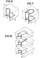
- a capillary sensor can be produced, as shown in FIG. 6, in the form of a groove made along the edge of the component from the connection pad 20. This groove is then metallized using a material having wetting properties with respect to the brazing alloy.
- the advantage of providing the capillary sensor, in the form of a groove, is to increase the surface of the capillary sensor.
- the metallized groove 27 is extended on the face 24, by a metallized area 29 of the same type as the groove. The capture of the solder when passing over the solder wave is thus improved.
- a capillary sensor according to the invention has been shown in the form of a jumper 27 plugged in on the edge of the component 2, exerting a slight pressure on the face 24 and the connection pad 20.
- component assembly 2, jumper 27, stud connection 20 and connection pad 11 are coated with solder.
- the invention also makes it possible to solve the problems of connection of components with several layers.
- the component of FIG. 10 has three layers 2, 4 and 6.
- Layer 2 carries on its face 26, a connection pad 20.
- Layer 4 has a connection 42 of the internal circuit to the component.
- a groove 27 leading to the stud 20 is formed in the edge of the layer 2 and is metallized.
- metallized grooves 41 and 61 are formed in correspondence with the groove 27 in layers 4 and 6.
- metallized bases 29, 40, 43 and 60 are produced on either side of layers 2, 4 , 6, around the grooves.
- a metallized base 62 is also produced on the upper face of the layer 6. The different layers are then stacked, pressed and glued one against the other.
- the bases 29, 40, 43 and 63 provide metallic continuity of the groove to improve the flow of the solder along the groove during the transition to the solder wave.
- the capillary sensor can also be supported by another part than the component itself.
- the capillary sensor on the face 10 of the printed circuit board 1, there are elements specially designed for this use such as the element 50.
- the element 50 On the element 50 is deposited a metallized strip 51, 52, 53 connecting the top of the element 50 to the connection pad 11 of the card.
- the height h of the element 50 is such that depending on the wave, the height of the components and the position of the element 50 relative to the components, the part 51 of metallized strip is reached by the solder wave .
- several capillary sensors can be provided on an element 50.
- an element 50 can serve several components.
Landscapes
- Engineering & Computer Science (AREA)
- Manufacturing & Machinery (AREA)
- Microelectronics & Electronic Packaging (AREA)
- Mechanical Engineering (AREA)
- Electric Connection Of Electric Components To Printed Circuits (AREA)
Abstract
Description
- L'invention concerne un procédé de brasage à la vague permettant de braser, sur une carte de circuits imprimés, des composants dont les broches de connexion ne traversent pas la carte. L'invention concerne également des capteurs capillaires mettant en oeuvre ce procédé.
- Selon une technique courante, la connexion d'un composant sur une carte de circuits imprimés se fait à l'aide de broches appartenant au composant, traversant la carte de circuits imprimés par des trous de connexion, et par brasage des broches à des pastilles de connexion situés sur la face opposée de la carte. L'opération de brasage se fait par passage de la carte au dessus d'une vague de brasure en fusion, la face de la carte portant les pastilles de connexion entrant au contact, lors de ce passage, avec la vague de brasure.
- Selon une technique récente de connexion, les broches des composants ne traversent pas la carte de circuits imprimés. Les composants possèdent des plots de connexion qui sont mis simplement en contact avec des plots de connexions de la carte de circuits imprimés et auxquels ils sont ensuite brasés. Ce brasage peut être effectué également par passage sur une vague de brasure. Pour celà, les composants sont au préalable mis en position sur la carte et immobilisés, les plots de connexion des composants étant en contact avec les plots de connexion de la carte. La carte est ensuite passée au dessus de la vague de brasure, la face portant les plots de connexion ainsi que les composants entrant en contact avec la vague de brasure. Lors de ce passage, chaque composant baigne donc dans le bain de brasure en fusion. La face du composant qui attaque la vague de brasure est, en principe, en contact en entier avec la brasure. Les parties métallisées de cette face sont mouillées par la brasure et le brasage des plots de connexion de cette face du composant avec les plots de la carte peut se faire. Par contre, en raison de la température du bain de brasure, la carte doit passer à une vitesse suffisante, pour éviter l'échauffement des composants. De ce fait, l'écoulement du fluide de brasure sur les côtés et sur la face arrière de chaque composant est tel que certaines parties du composant peuvent ne pas être en contact avec la brasure. Le brasage des plots de connexion peut ne pas être assuré.
- L'invention se fixe pour but un procédé permettant d'assurer un brasage de tous les plots de connexion d'un composant sur les plots de connexion d'un substrat. Elle fournit en outre un capteur capillaire de brasure permettant de mettre en oeuvre ce procédé.
- L'invention concerne donc un procédé de brasage à la vague permettant de braser les plots de connexion d'un composant à des plots de connexion d'un substrat dans lequel le composant et ses plots de connexion sont situés d'un même côté du substrat que les plots de connexion de ce substrat, caractérisé en ce qu'il comprend les étapes suivantes :
- - création de capteurs capillaires de brasure aboutissant aux points des plots de connexion du composant et des plots de connexion du substrat et émergeant de la surface supérieure du composant par rapport au substrat ;
- - collage du composant sur le substrat avec les plots de connexion du composant en contact avec les plots de connexion du substrat ;
- - passage de l'ensemble substrat-composant ainsi constitué dans la vague de brasure de telle façon que celle-ci touche les capteurs capillaires de brasure ;
- - captage de brasure par les capteurs capillaires ;
- - propagation de la brasure par capillarité jusqu'aux plots de connexion du composant et du substrat ;
- - soudure des plots de connexion du composant aux plots de connexion du substrat.
- L'invention concerne également un capteur capillaire de brasure permettant de mettre en oeuvre ce procédé.
- L'invention sera mieux comprise et d'autres caractéristiques apparaîtront à l'aide de la description qui va suivre et des figures annexées parmi lesquelles :
- - les figures 1 à 3 sont des schémas explicatifs d'un système de brasage à la vague de l'art connu auxquels s'applique l'invention ;
- - les figures 4 et 5 représentent des schémas explicatifs du procédé selon l'invention ;
- - les figures 6 et 7 représentent des exemples de capteurs capillaires de brasure selon l'invention ;
- - les figures 8 et 9 représentent une exemple de réalisation d'un autre capteur capillaire selon l'invention ;
- - la figure 10 représente un capteur capillaire de brasure selon l'invention pour circuits à plusieurs couches ;
- - la figure 11 représente une variante d'un capteur capillaire de brasure.
- En se reportant aux figures 1 à 3, on va décrire un système de brasage à la vague. Sur la figure 1, on trouve une carte de circuits imprimés 1 équipée d'un composant 2. Une vague d'alliage de brasage en fusion 3 est produite par un flux d'alliage 30 canalisé par deux pièces 31 et 32. Cette vague effleure un plan P. La carte 1 est disposée sur un dispositif de transfert non représenté et connu de la technique. Elle est déplacée selon le sens indiqué par la flèche F avec sa face 10 à souder située dans le P.
- La carte 1 possède sur sa face 10 des circuits imprimés non représentés et des plots de connexion 11 et 12. Le composant 2 est collé à la face 10 de la carte 1 par un bossage 22. Le composant 2 possède en outre, sur sa face 26, des plots de connexion tel que 20 et 21 qui sont mis en contact (ou au voisinage) des plots de connexion 11 et 12 de la carte 1.
- Lorsque la carte 1 passe sur la vague de brasure 3, celle-ci balaye la surface de la carte. La brasure mouille les parties métalliques avec lesquelles elle entre en contact et les pièces métalliques, tels que plots de connexion, sont brasées. Cependant, comme on le voit sur la figure, le composant baigne dans la brasure en fusion durant le déplacement de la carte. On a donc intérêt à ce que ce déplacement soit suffisamment rapide. Il se trouve alors, en raison de l'écoulement du fluide de brasure autour du composant 2, que des parties du composant ne sont pas mis en contact avec la brasure. Sur la figure 2, on peut voir que la face avant 23 du composant ainsi que les plots de connexion 12 et 21 sont baignés dans la brasure, il en est de même de la face 24 du composant. Par contre, à la suite de la face arrière 25 par rapport au mouvement selon la flèche F se créé une zone 33 sans brasure. Les plots de connexion 11 et 20 ne peuvent donc pas être brasés. De même comme on peut le voir sur la figure 3, il peut se produire une absence de brasure dans la zone 34 de part et d'autre des faces latérales 27 et 37 du composant.
- C'est pourquoi l'invention, avant l'étape de passage de la carte 2 sur la vague de brasure, prévoit de placer des capteurs capillaires de brasures reliant chaque plot, tel que 20, à la face 24 du composant. Ainsi lors du passage de la carte 2 sur la vague 3, la brasure en balayant la face 24 du composant entre en contact avec le capteur capillaire, le mouille, et progresse par capillarité vers les plots de connexion.
- Sur la figure 4 on a représenté un capteur capillaire 27 reliant le plot de connexion 20 à la face 24 du composant. Pour des questions d'uniformité de fabrication un capteur 28, bien qu'il ne soit indispensable, relie le plot de connexion 21 à la face 24. La carte 1, se déplaçant selon la flèche F, en mouvement relatif, la brasure se déplace par rapport au composant selon la flèche A. Lorsque la brasure touche le capteur capillaire 27, elle mouille celle-ci et tend à se répandre sur toute sa surface. En particulier, elle progresse selon la flèche B vers des plots de connexion 20 et 11 qu'elle brase ensemble.
- Sur la figure 5, représentant une portion du composant 2, le parcours de la brasure est représenté plus en détail. En effet, la brasure tendant à mouiller les parties métallisées, elle suit la flèche B et arrivée aux plots de connexion 11 et 20, elle les recouvre uniformément.
- Un capteur capillaire peut être réalisé, comme cela est représenté en figure 6, sous forme d'une cannelure pratiquée le long de la tranche du composant à partir du plot de connexion 20. Cette cannelure est ensuite métallisée à l'aide d'un matériau ayant des propriétés mouillantes vis-à-vis de l'alliage de brasage. L'avantage de prévoir le capteur capillaire, en forme de cannelure, est d'augmenter la surface du capteur capillaire.
- Sur la figure 7, la cannelure métallisée 27 est prolongée sur la face 24, par une plage métallisée 29 de même type que la cannelure. Le captage de la brasure lors du passage sur la vague de brasure est ainsi améliorée.
- Sur la figure 8, un capteur capillaire selon l'invention a été représenté sous forme d'un cavalier 27 embroché sur la tranche du composant 2, exerçant une légère pression sur la face 24 et le plot de connexion 20. Après le passage à la vague de brasure, l'ensemble composant 2, cavalier 27, plot de connexion 20 et plot de connexion 11 se trouvent enrobés de brasure.
- L'invention permet par ailleurs de résoudre les problèmes de connexion des composants à plusieurs couches. Le composant de la figure 10 comporte trois couches 2, 4 et 6.
- La couche 2 porte sur sa face 26, un plot de connexion 20. La couche 4 possède une connexion 42 de circuit interne au composant. Une cannelure 27 aboutissant au plot 20 est pratiquée dans la tranche de la couche 2 et est métallisée. De même, des cannelures métallisées 41 et 61 sont pratiquées en correspondance de la cannelure 27 dans les couches 4 et 6. De plus, des embases métallisées 29, 40, 43 et 60 sont réalisées de part et d'autre des couches 2, 4, 6, autour des cannelures. Une embase métallisée 62 est également réalisée sur la face supérieure de la couche 6. Les différentes couches sont ensuite empilées, pressées et collées l'une contre l'autre. Les embases 29, 40, 43 et 63 assurent une continuité métallique de la cannelure pour améliorer l'écoulement de la brasure le long de la cannelure lors du passage à la vague de brasure.
- Le capteur capillaire peut être également supporté par une autre pièce que le composant lui-même. Par exemple, sur la face 10 de la carte de circuits imprimés 1, on dispose des éléments conçus spécialement pour cet usage tels que l'élément 50. Sur l'élément 50 est déposée une bande métallisée 51, 52, 53 reliant le sommet de l'élément 50 au plot de connexion 11 de la carte. La hauteur h de l'élément 50 est telle qu'en fonction de la vague, de la hauteur des composants et de la position de l'élément 50 par rapport aux composants, la partie 51 de bande métallisée soit atteinte par la vague de brasure. Comme représenté sur la figure 11, plusieurs capteurs capillaires peuvent être prévus sur un élément 50. De même, un élément 50 peut desservir plusieurs composants.
Claims (10)
Applications Claiming Priority (2)
| Application Number | Priority Date | Filing Date | Title |
|---|---|---|---|
| FR8318128A FR2555010B1 (fr) | 1983-11-15 | 1983-11-15 | Procede de brasage a la vague et capteur capillaire de brasure mettant en oeuvre ce procede |
| FR8318128 | 1983-11-15 |
Publications (3)
| Publication Number | Publication Date |
|---|---|
| EP0145557A2 true EP0145557A2 (fr) | 1985-06-19 |
| EP0145557A3 EP0145557A3 (en) | 1985-07-10 |
| EP0145557B1 EP0145557B1 (fr) | 1989-07-26 |
Family
ID=9294121
Family Applications (1)
| Application Number | Title | Priority Date | Filing Date |
|---|---|---|---|
| EP84402304A Expired EP0145557B1 (fr) | 1983-11-15 | 1984-11-13 | Procédé de brasage à la vague et capteur capillaire de brasure mettant en oeuvre ce procédé |
Country Status (3)
| Country | Link |
|---|---|
| EP (1) | EP0145557B1 (fr) |
| DE (1) | DE3479178D1 (fr) |
| FR (1) | FR2555010B1 (fr) |
Cited By (3)
| Publication number | Priority date | Publication date | Assignee | Title |
|---|---|---|---|---|
| EP0210560A3 (fr) * | 1985-07-27 | 1987-05-27 | GRUNDIG E.M.V. Elektro-Mechanische Versuchsanstalt Max Grundig holländ. Stiftung & Co. KG. | Procédé de soudage d'un circuit intégré à une plaquette de circuit |
| FR2613898A1 (fr) * | 1987-04-13 | 1988-10-14 | Siame Electronique Sa | Procede de soudage de composants pour montage en surface (cms) sur circuit imprime |
| EP0245188A3 (fr) * | 1986-04-28 | 1989-12-06 | Société Talco | Procédé de brasage de composants de surface sur une carte imprimée |
Family Cites Families (4)
| Publication number | Priority date | Publication date | Assignee | Title |
|---|---|---|---|---|
| GB811509A (en) * | 1954-11-22 | 1959-04-08 | Ibm | Improvements relating to printed circuit connections |
| FR1369630A (fr) * | 1963-09-06 | 1964-08-14 | Atomic Energy Authority Uk | Système de brasure pour joints |
| JPS5724775U (fr) * | 1980-07-17 | 1982-02-08 | ||
| DE3231056A1 (de) * | 1982-08-20 | 1984-02-23 | Siemens AG, 1000 Berlin und 8000 München | Verfahren zum aufbringen von unbedrahteten bauelementen auf leiterplatten |
-
1983
- 1983-11-15 FR FR8318128A patent/FR2555010B1/fr not_active Expired
-
1984
- 1984-11-13 EP EP84402304A patent/EP0145557B1/fr not_active Expired
- 1984-11-13 DE DE8484402304T patent/DE3479178D1/de not_active Expired
Cited By (3)
| Publication number | Priority date | Publication date | Assignee | Title |
|---|---|---|---|---|
| EP0210560A3 (fr) * | 1985-07-27 | 1987-05-27 | GRUNDIG E.M.V. Elektro-Mechanische Versuchsanstalt Max Grundig holländ. Stiftung & Co. KG. | Procédé de soudage d'un circuit intégré à une plaquette de circuit |
| EP0245188A3 (fr) * | 1986-04-28 | 1989-12-06 | Société Talco | Procédé de brasage de composants de surface sur une carte imprimée |
| FR2613898A1 (fr) * | 1987-04-13 | 1988-10-14 | Siame Electronique Sa | Procede de soudage de composants pour montage en surface (cms) sur circuit imprime |
Also Published As
| Publication number | Publication date |
|---|---|
| FR2555010A1 (fr) | 1985-05-17 |
| EP0145557A3 (en) | 1985-07-10 |
| DE3479178D1 (en) | 1989-08-31 |
| EP0145557B1 (fr) | 1989-07-26 |
| FR2555010B1 (fr) | 1986-08-29 |
Similar Documents
| Publication | Publication Date | Title |
|---|---|---|
| FR2769390A1 (fr) | Procede de fabrication de cartes a puce aptes a assurer un fonctionnement a contact et sans contact, et de cartes a puce sans contact | |
| KR100959847B1 (ko) | 전자 장치 및 전자 장치의 제조 방법 | |
| FR2591815A1 (fr) | Structure d'interconnexion de plot de soudage | |
| FR2634616A1 (fr) | Procede de montage de micro-composants electroniques sur un support et produit realisable par le procede | |
| EP0717442B1 (fr) | Support de connexion d'un circuit intégré à un autre support par l'intermédiare de boules | |
| FR2761527A1 (fr) | Procede de fabrication de carte sans contact avec connexion d'antenne par fils soudes | |
| FR2541044A1 (fr) | Procede de montage d'une plaquette de circuit integre sur un substrat | |
| EP0145557B1 (fr) | Procédé de brasage à la vague et capteur capillaire de brasure mettant en oeuvre ce procédé | |
| CA2646813A1 (fr) | Dispositif radiofrequence | |
| EP0351268A1 (fr) | Procédé de soudure des fils de connexions extérieures sur un composant électronique | |
| JP4018702B2 (ja) | 磁気ヘッドアッセンブリ | |
| EP0115460B1 (fr) | Carte souple de circuit imprimé, procédé de modification d'une carte de circuit imprimé, et carte modifiée de circuit imprimé | |
| EP0221809B1 (fr) | Circuit hybride et procédé de fabrication d'un tel circuit | |
| EP0895627B1 (fr) | Ensemble electronique comprenant une unite electronique reliee a une bobine | |
| EP1350418A1 (fr) | Procede de realisation d'interconnexion dans un circuit imprime multicouches | |
| EP4293569B1 (fr) | Inlay pour document electronique, procédé de fabrication d'un document électronique comportant un tel inlay, et document électronique obtenu | |
| FR2550906A1 (fr) | Carte de circuit imprime a couches multiples et son procede de fabrication | |
| EP0360647A1 (fr) | Dispositif de codage notamment pour carte à circuits intégrés | |
| FR2711830A1 (fr) | Assemblage patin de vol/bras-ressort à plots de soudures composités et procédé de réalisation. | |
| CH643089A5 (en) | Method of mounting an integrated circuit board on a substrate | |
| FR2571547A1 (fr) | Circuit hybride reportable sur un support comportant un reseau d'interconnexion a haute densite | |
| FR2693339A1 (fr) | Procédé de liaison et de fixation de composants à broches sur un circuit imprimé souple, et circuit ainsi obtenu. | |
| FR3145834A1 (fr) | Composant de liaison de signaux de boîtier de semi-conducteur de puissance et module à semi-conducteur | |
| FR2588124A1 (fr) | Procede de connexion d'un circuit electronique sur un cable connecteur plat et souple | |
| EP0901165A1 (fr) | Boítier à microcircuit intégré et procédé de montage de microcircuit intégré |
Legal Events
| Date | Code | Title | Description |
|---|---|---|---|
| PUAI | Public reference made under article 153(3) epc to a published international application that has entered the european phase |
Free format text: ORIGINAL CODE: 0009012 |
|
| PUAL | Search report despatched |
Free format text: ORIGINAL CODE: 0009013 |
|
| AK | Designated contracting states |
Designated state(s): DE GB IT NL |
|
| AK | Designated contracting states |
Designated state(s): DE GB IT NL |
|
| 17P | Request for examination filed |
Effective date: 19851114 |
|
| 17Q | First examination report despatched |
Effective date: 19871021 |
|
| RAP3 | Party data changed (applicant data changed or rights of an application transferred) |
Owner name: THOMSON-CSF |
|
| GRAA | (expected) grant |
Free format text: ORIGINAL CODE: 0009210 |
|
| AK | Designated contracting states |
Kind code of ref document: B1 Designated state(s): DE GB IT NL |
|
| ITF | It: translation for a ep patent filed | ||
| REF | Corresponds to: |
Ref document number: 3479178 Country of ref document: DE Date of ref document: 19890831 |
|
| GBT | Gb: translation of ep patent filed (gb section 77(6)(a)/1977) | ||
| PLBE | No opposition filed within time limit |
Free format text: ORIGINAL CODE: 0009261 |
|
| STAA | Information on the status of an ep patent application or granted ep patent |
Free format text: STATUS: NO OPPOSITION FILED WITHIN TIME LIMIT |
|
| 26N | No opposition filed | ||
| PGFP | Annual fee paid to national office [announced via postgrant information from national office to epo] |
Ref country code: DE Payment date: 19921009 Year of fee payment: 9 |
|
| PGFP | Annual fee paid to national office [announced via postgrant information from national office to epo] |
Ref country code: GB Payment date: 19921014 Year of fee payment: 9 |
|
| ITTA | It: last paid annual fee | ||
| PGFP | Annual fee paid to national office [announced via postgrant information from national office to epo] |
Ref country code: NL Payment date: 19921130 Year of fee payment: 9 |
|
| PG25 | Lapsed in a contracting state [announced via postgrant information from national office to epo] |
Ref country code: GB Effective date: 19931113 |
|
| PG25 | Lapsed in a contracting state [announced via postgrant information from national office to epo] |
Ref country code: NL Effective date: 19940601 |
|
| GBPC | Gb: european patent ceased through non-payment of renewal fee |
Effective date: 19931113 |
|
| NLV4 | Nl: lapsed or anulled due to non-payment of the annual fee | ||
| PG25 | Lapsed in a contracting state [announced via postgrant information from national office to epo] |
Ref country code: DE Effective date: 19940802 |