EP0146181A2 - Halbleiteranordnung mit einem zusammengefassten Bipolar-Feldeffekttransistor - Google Patents
Halbleiteranordnung mit einem zusammengefassten Bipolar-Feldeffekttransistor Download PDFInfo
- Publication number
- EP0146181A2 EP0146181A2 EP84201803A EP84201803A EP0146181A2 EP 0146181 A2 EP0146181 A2 EP 0146181A2 EP 84201803 A EP84201803 A EP 84201803A EP 84201803 A EP84201803 A EP 84201803A EP 0146181 A2 EP0146181 A2 EP 0146181A2
- Authority
- EP
- European Patent Office
- Prior art keywords
- region
- conductivity type
- layer
- field effect
- effect transistor
- Prior art date
- Legal status (The legal status is an assumption and is not a legal conclusion. Google has not performed a legal analysis and makes no representation as to the accuracy of the status listed.)
- Granted
Links
Images

Classifications
-
- H—ELECTRICITY
- H10—SEMICONDUCTOR DEVICES; ELECTRIC SOLID-STATE DEVICES NOT OTHERWISE PROVIDED FOR
- H10D—INORGANIC ELECTRIC SEMICONDUCTOR DEVICES
- H10D30/00—Field-effect transistors [FET]
- H10D30/60—Insulated-gate field-effect transistors [IGFET]
- H10D30/64—Double-diffused metal-oxide semiconductor [DMOS] FETs
- H10D30/65—Lateral DMOS [LDMOS] FETs
-
- H—ELECTRICITY
- H10—SEMICONDUCTOR DEVICES; ELECTRIC SOLID-STATE DEVICES NOT OTHERWISE PROVIDED FOR
- H10D—INORGANIC ELECTRIC SEMICONDUCTOR DEVICES
- H10D12/00—Bipolar devices controlled by the field effect, e.g. insulated-gate bipolar transistors [IGBT]
- H10D12/411—Insulated-gate bipolar transistors [IGBT]
-
- H—ELECTRICITY
- H10—SEMICONDUCTOR DEVICES; ELECTRIC SOLID-STATE DEVICES NOT OTHERWISE PROVIDED FOR
- H10D—INORGANIC ELECTRIC SEMICONDUCTOR DEVICES
- H10D62/00—Semiconductor bodies, or regions thereof, of devices having potential barriers
- H10D62/10—Shapes, relative sizes or dispositions of the regions of the semiconductor bodies; Shapes of the semiconductor bodies
- H10D62/102—Constructional design considerations for preventing surface leakage or controlling electric field concentration
- H10D62/103—Constructional design considerations for preventing surface leakage or controlling electric field concentration for increasing or controlling the breakdown voltage of reverse-biased devices
- H10D62/105—Constructional design considerations for preventing surface leakage or controlling electric field concentration for increasing or controlling the breakdown voltage of reverse-biased devices by having particular doping profiles, shapes or arrangements of PN junctions; by having supplementary regions, e.g. junction termination extension [JTE]
- H10D62/106—Constructional design considerations for preventing surface leakage or controlling electric field concentration for increasing or controlling the breakdown voltage of reverse-biased devices by having particular doping profiles, shapes or arrangements of PN junctions; by having supplementary regions, e.g. junction termination extension [JTE] having supplementary regions doped oppositely to or in rectifying contact with regions of the semiconductor bodies, e.g. guard rings with PN or Schottky junctions
-
- H—ELECTRICITY
- H10—SEMICONDUCTOR DEVICES; ELECTRIC SOLID-STATE DEVICES NOT OTHERWISE PROVIDED FOR
- H10D—INORGANIC ELECTRIC SEMICONDUCTOR DEVICES
- H10D84/00—Integrated devices formed in or on semiconductor substrates that comprise only semiconducting layers, e.g. on Si wafers or on GaAs-on-Si wafers
- H10D84/101—Integrated devices comprising main components and built-in components, e.g. IGBT having built-in freewheel diode
- H10D84/121—BJTs having built-in components
-
- H—ELECTRICITY
- H10—SEMICONDUCTOR DEVICES; ELECTRIC SOLID-STATE DEVICES NOT OTHERWISE PROVIDED FOR
- H10D—INORGANIC ELECTRIC SEMICONDUCTOR DEVICES
- H10D84/00—Integrated devices formed in or on semiconductor substrates that comprise only semiconducting layers, e.g. on Si wafers or on GaAs-on-Si wafers
- H10D84/40—Integrated devices formed in or on semiconductor substrates that comprise only semiconducting layers, e.g. on Si wafers or on GaAs-on-Si wafers characterised by the integration of at least one component covered by groups H10D12/00 or H10D30/00 with at least one component covered by groups H10D10/00 or H10D18/00, e.g. integration of IGFETs with BJTs
- H10D84/401—Combinations of FETs or IGBTs with BJTs
- H10D84/403—Combinations of FETs or IGBTs with BJTs and with one or more of diodes, resistors or capacitors
- H10D84/406—Combinations of FETs or IGBTs with vertical BJTs and with one or more of diodes, resistors or capacitors
-
- H—ELECTRICITY
- H10—SEMICONDUCTOR DEVICES; ELECTRIC SOLID-STATE DEVICES NOT OTHERWISE PROVIDED FOR
- H10W—GENERIC PACKAGES, INTERCONNECTIONS, CONNECTORS OR OTHER CONSTRUCTIONAL DETAILS OF DEVICES COVERED BY CLASS H10
- H10W15/00—Highly-doped buried regions of integrated devices
-
- H—ELECTRICITY
- H10—SEMICONDUCTOR DEVICES; ELECTRIC SOLID-STATE DEVICES NOT OTHERWISE PROVIDED FOR
- H10W—GENERIC PACKAGES, INTERCONNECTIONS, CONNECTORS OR OTHER CONSTRUCTIONAL DETAILS OF DEVICES COVERED BY CLASS H10
- H10W15/00—Highly-doped buried regions of integrated devices
- H10W15/01—Manufacture or treatment
-
- H—ELECTRICITY
- H10—SEMICONDUCTOR DEVICES; ELECTRIC SOLID-STATE DEVICES NOT OTHERWISE PROVIDED FOR
- H10D—INORGANIC ELECTRIC SEMICONDUCTOR DEVICES
- H10D62/00—Semiconductor bodies, or regions thereof, of devices having potential barriers
- H10D62/10—Shapes, relative sizes or dispositions of the regions of the semiconductor bodies; Shapes of the semiconductor bodies
- H10D62/13—Semiconductor regions connected to electrodes carrying current to be rectified, amplified or switched, e.g. source or drain regions
- H10D62/149—Source or drain regions of field-effect devices
- H10D62/151—Source or drain regions of field-effect devices of IGFETs
- H10D62/156—Drain regions of DMOS transistors
- H10D62/157—Impurity concentrations or distributions
-
- H—ELECTRICITY
- H10—SEMICONDUCTOR DEVICES; ELECTRIC SOLID-STATE DEVICES NOT OTHERWISE PROVIDED FOR
- H10D—INORGANIC ELECTRIC SEMICONDUCTOR DEVICES
- H10D62/00—Semiconductor bodies, or regions thereof, of devices having potential barriers
- H10D62/10—Shapes, relative sizes or dispositions of the regions of the semiconductor bodies; Shapes of the semiconductor bodies
- H10D62/17—Semiconductor regions connected to electrodes not carrying current to be rectified, amplified or switched, e.g. channel regions
- H10D62/351—Substrate regions of field-effect devices
- H10D62/357—Substrate regions of field-effect devices of FETs
- H10D62/364—Substrate regions of field-effect devices of FETs of IGFETs
- H10D62/371—Inactive supplementary semiconductor regions, e.g. for preventing punch-through, improving capacity effect or leakage current
Definitions
- the invention relates to a combined bipolar-field effect transistor RESURF device, comprising
- the breakdown characteristics of high-voltage semiconductor devices generally can be improved by using the REduced SURface Field (or RESURF) technique, as described in "High Voltage Thin Layer Devices (RESURF Devices)", “International Electronic Devices Meeting Technical Digest", December, 1979, pages 238-240, by Appels et al, and U.S. Patent No. 4,292,642, incorporated herein by reference.
- RESURF REduced SURface Field
- the RESURF technique was applied to lateral double-diffused MOS transistors, as described in U.S. Patent 4,300,150 and also in "Lateral DMOS Power Transistor Design", “IEEE Electron Device Letters", Vol. EDL-1, pages 51-53, April 1980, by Colak et al, and the result was a substantial improvement in device characteristics.
- high-voltage DMOS devices there is normally a trade-off between breakdown voltage and on-resistance, with the goal being to increase the breakdown voltage level while maintaining a relatively low on-resistance.
- an improvement e.g.
- a combined bipolar-field effect transistor RESURF device as described in the preamble is characterized in that the device comprises a lightly-doped epitaxial 'buried layer of said first conductivity type on said major surface of the substrate and having a doping level at least an order of magnitude less than that of said substrate.
- the improved on-resistance and switching characteristics mentioned above are achieved by using minority carriers for conductivity modulation, by exploiting the vertical base widening phenomenon, and by using a double-epi construction to confine minority carriers.
- These improvements are made possible by the incorporation of the lightly-doped epitaxial buried layer, which is located between the substrate and the epitaxial surface layer of the device.
- the device according to the invention comprises a highly-doped buried region of said second conductivity type located beneath said base region and sandwiched between said epitaxial buried layer of the first conductivity type and said epitaxial surface layer of the second conductivity type.
- a highly-doped buried region reduces the base drive current and the internal power dissipation of the device.
- Devices in accordance with the invention may also include a buried annular region of the first conductivity type around and in contact with the highly-doped buried region, as well as a surface-adjoining annular region of the first conductivity type adjacent the base region.
- the various embodiments described above may additionally include a highly-doped buried layer, of the same conductivity type as that of the substrate, located in the substrate at its intersection with the lightly-doped epitaxial buried layer.
- This highly-doped buried layer serves to increase conductivity modulation in the lightly-doped epitaxial buried layer and also to enhance confinement of carriers to the lightly-doped epitaxial buried layer.
- Such devices not only require reduced base drive for a given level of on-resistance and provide reduced internal power dissipation, but also provide improved isolation with respect to adjacent devices on the same substrate and improved switching speed.
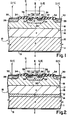
- Fig. 1 of the drawing shows a combined bipolar-field effect transistor RESURF device which is suitable for high-voltage switching applications. It should be noted that the drawing is not to scale, and in particular that the vertical dimensions are exaggerated for improved clarity. Additionally, like parts are designated with like reference numerals in the figures, and semiconductor regions of the same conductivity type are shown hatched in the same direction.
- a combined bipolar-field effect transistor RESURF device 10 has a semiconductor substrate 11 with a major surface 12 on its upper side and a substrate electrode 13 on its lower side.
- the substrate 11 is of p conductivity type and has a doping level of at least about 3x10 15 atoms/em 3 .
- a lightly-doped epitaxial buried layer 16 is located on surface 12 of the substrate and has a doping level of at least an order of magnitude (a factor of 10 times) less than that of the substrate.
- the lightly-doped epitaxial buried layer here is of ⁇ (i.e. p-) conductivity type with a doping level of about 3x10 14 atoms/cm and a thickness of about 30 microns.
- An epitaxial surface layer 18 of n conductivity type is located on the upper surface 17 of ⁇ layer 16, and has a doping concentration N and thickness d selected in accordance with the REduced SURface Field (RESURF) technique, meaning that the total doping concentration per unit area of the layer (Nxd) is of the order of about 10 12 atoms per square cm.
- the epitaxial surface layer 18 has a doping level of about 10 15 atoms/cm 3 and a thickness of about 10 microns.
- the active regions of the combined bipolar-field effect transistor RESURF device are formed at the upper surface of epitaxial surface layer 18.
- a surface-adjoining base region 20 of p conductivity type and a doping level of about 10 17 atoms/cm 3 is provided with a base electrode 22 and a surface-adjoining source/ emitter region 24 of n+ conductivity type semiconductor material, with region 24 serving as both the source and the emitter of the combined bipolar-field effect transistor device.
- Region 24 is provided with a source/emitter electrode 26 connected to the upper surface of the region.
- a drain/collector region 28 of n+ conductivity type is provided adjacent the surface of the epitaxial surface layer 18 and is spaced apart from the base region 20, with a drain/collector electrode 30 connected to the upper surface of the drain/collector region.
- a lateral npn bipolar transistor is integrally formed with a lateral MOS field effect transistor.
- a surface-adjoining channel region 32 is located between source/emitter region 24 and drain/collector region 28, and is at least partly located in that portion of the base region which is adjacent to the drain/collector region.
- This latter-mentioned portion of the channel region 24 is covered by an insulating layer 34 of a material such as silicon dioxide or other suitable insulating material, with a gate electrode 36 being provided on the insulating layer 34 and over at least that part of the channel region which is in the base region 20. Since the various active regions of the device described above are formed in a conventional manner, they will not be discussed in further detail.
- the improved operational features of the present invention are achieved by using minority carriers for conductivity modulation and by exploiting the vertical base widening phenomenon typical of lateral RESURF devices to obtain lower specific on-resistances and increased yield for a given current and voltage rating. Additionally, the configuration of this device does not compromise the attributes of low input capacitance and ease of integration which are characteristic of devices of this general type.
- the-jf layer 16 serves as the substrate for purposes of blocking voltage, and, during the "off" state, this layer is fully depleted.
- a vertical pnp transistor is formed from regions of p layers 11 and 16, n layer 18 and p region 20. In the "on" state, layers 16 and 18 will be conductivity modulated by minority carriers.
- base and gate drive signals are applied to electrodes 22 and 36, respectively. This first activates the field effect transistor, and then, following a short delay, the lateral npn bipolar transistor switches "on". Due to the existence of a low-resistance channel region along the surface of the device, the lateral transistor switches immediately into saturation, with both the base-emitter and base-collector junctions forward biased. The forward biasing of the base-collector junction in turn triggers the vertical pnp transistor discussed above, and hole current flows to the substrate.
- the intervening layer 16 region becomes heavily conductivity modulated.
- the voltage required to maintain this situation is now dropped across the substrate resistance alone.
- the base widening phenomenon spreads laterally through the 7C layer.
- lateral base widening effects in the lateral npn bipolar transistor become significant, so that eventually the entire extended epitaxial layer (layers 16 and 18) becomes further modulated due to the combined effects of both vertical and lateral base widening.
- the effective cross-sectional area of the device is increased, since layer 16 in effect acts to extend the epitaxial surface layer. Furthermore, the entire extended epitaxial layer (16, 18) is conductivity modulated. As a result, the on-resistance of the device is dramatically reduced, since these two effects are nearly multiplicative in their influence on the conductive-state resistance of the device. While the device is in this conductive state, the carriers in the modulated layer 16 and the epitaxial surface layer 18 are maintained by a recombination current from the base region 20. Since the lifetime of the high- resistivity region is large, the recombination current will be small in comparison to the current delivered to the external load, thus enhancing device efficiency.
- the present invention also permits more design flexibility in the location of emitting and collecting regions, since these regions no longer need be alternated as in conventional lateral transistor designs. Since layer 16 is converted to n conductivity type through the base widening phenomenon, this layer may act as a low resistance buried collector region, thus permitting emitting regions to be arranged for optimum efficiency and maximum emitting surface area and packing density. As a final advantage, the present configuration also reduces the number of regions that experience high electric fields, which increases overall device yield.
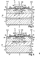
- FIG. 2 A second embodiment of a combined bipolar-field effect transistor RESURF device is shown in Fig. 2.
- This device differs from the device shown in Fig. 1 in that a highly-doped p+ conductivity type buried layer 14 is provided in the substrate 11 at major surface 12.
- the device of Fig. 2 corresponds to the device previously described with reference to Fig. 1, with like reference numerals being used to designate like regions in the two figures. Accordingly, the description of Fig. 2 will be limited to the highly-doped buried layer and its effect upon device performance.
- a highly-doped p+ buried layer 14 is provided at major surface 12 of the substrate 11.
- This highly-doped p+ buried layer has a doping level of about 10 18 atoms/cm and a thickness of about 5 microns.
- the highly-doped buried layer 14 serves to increase the injection efficiency of the substrate 11 relative to that of the epitaxial surface layer 18, thereby increasing conductivity modulation of layer 16 and creating a barrier to electron flow into the substrate, thus confining the base widening phenomenon to layer 16 where it is mot effective. As a result, improved device speed and better lateral isolation may be obtained.
- buried layer 14 is shown only in Fig. 2 and 3, the devices shown in Figs. 1, 4 and 5 may all be fabricated either with or without this buried layer.
- Fig. 3 of the drawing shows a third embodiment of the device according to the invention.
- This device differs from the device shown in Fig. 2 in that a highly-doped buried region 19 is located beneath the base region 20 and sandwiched between the epitaxial buried layer 16 and the epitaxial surface layer 18 at the surface 17.
- the device of Fig. 3 corresponds to the device previously described with reference to Fig. 2, the same reference numerals being used for corresponding regions and parts.
- buried region 19 is of n+ conductivity type and has a doping level in the range of about 10 18 - 10 20 atoms/cm and a thickness in the range of about 1-2 microns.
- n+ buried region 19 acts as a barrier to holes, hole concentration gradients are increased in the region of the base, and the base widening effects are enhanced.
- the beta of the vertical transistor is reduced, so that hole current to the substrate is minimized. In this manner, the amount of base drive current for a desired on-resistance is reduced, and unwanted internal power dissipation is lowered. At the same time, desired hole current in the lateral direction is enchanced, thus improving lateral conductivity and lowering on-resistance. More particularly, the addition of buried layer 19 can reduce the required base drive current for a given level of on-resistance by a factor of two, so that a considerably smaller base drive power source may be used. Additionally, both operating speed and device isolation are improved by reducing vertical conductivity and enhancing lateral conductivity.
- a device as described above is additionally provided with a buried annular region 21 around and in contact with highly-doped buried region 19.
- the buried annular region is of p conductivity type and has a doping level in the range of about 3x10 15 - 1x10 16 atoms/cm 3 and a thickness in the range of about 1-2 microns.
- a device having buried regions 19 and 21 as described above is further provided with a surface-adjoining annular region 23 adjacent the base region 20.
- Region 23 in this example is of p conductivity type, with a doping level of about 10 16 atoms/cm3 and a thickness of about 1 micron.
- surface-adjoining annular region 23 serves several purposes. As an additional field-shaping layer, it improves the high voltage capabilities of the device. Additionally, in the "on" state it provides uniform conductivity modulation of the epitaxial surface layer and serves as an additional source of injected holes closer to the drain region. As a result, device efficiency and speed are further improved.
Landscapes
- Bipolar Transistors (AREA)
- Metal-Oxide And Bipolar Metal-Oxide Semiconductor Integrated Circuits (AREA)
Applications Claiming Priority (4)
| Application Number | Priority Date | Filing Date | Title |
|---|---|---|---|
| US56214583A | 1983-12-16 | 1983-12-16 | |
| US56214483A | 1983-12-16 | 1983-12-16 | |
| US562145 | 1983-12-16 | ||
| US562144 | 1983-12-16 |
Publications (3)
| Publication Number | Publication Date |
|---|---|
| EP0146181A2 true EP0146181A2 (de) | 1985-06-26 |
| EP0146181A3 EP0146181A3 (en) | 1986-03-12 |
| EP0146181B1 EP0146181B1 (de) | 1989-03-15 |
Family
ID=27072846
Family Applications (1)
| Application Number | Title | Priority Date | Filing Date |
|---|---|---|---|
| EP84201803A Expired EP0146181B1 (de) | 1983-12-16 | 1984-12-05 | Halbleiteranordnung mit einem zusammengefassten Bipolar-Feldeffekttransistor |
Country Status (4)
| Country | Link |
|---|---|
| EP (1) | EP0146181B1 (de) |
| JP (1) | JPS60153163A (de) |
| CA (1) | CA1220875A (de) |
| DE (1) | DE3477313D1 (de) |
Cited By (9)
| Publication number | Priority date | Publication date | Assignee | Title |
|---|---|---|---|---|
| EP0185415A3 (en) * | 1984-12-21 | 1988-08-31 | N.V. Philips' Gloeilampenfabrieken | Conductivity-enhanced combined lateral mos/bipolar transconductivity-enhanced combined lateral mos/bipolar transistor istor |
| US4926074A (en) * | 1987-10-30 | 1990-05-15 | North American Philips Corporation | Semiconductor switch with parallel lateral double diffused MOS transistor and lateral insulated gate transistor |
| US4939566A (en) * | 1987-10-30 | 1990-07-03 | North American Philips Corporation | Semiconductor switch with parallel DMOS and IGT |
| EP0426252A3 (en) * | 1989-11-01 | 1991-06-26 | Philips Electronic And Associated Industries Limited | A semiconductor device and method of manufacturing a semiconductor device |
| EP0438959A3 (en) * | 1990-01-23 | 1993-03-10 | International Business Machines Corporation | Semiconductor device structure employing a multi-level epitaxial structure and a method of manufacturing same |
| EP0599221A1 (de) * | 1992-11-20 | 1994-06-01 | Hitachi, Ltd. | IGBT mit Bipolartransistor |
| DE9419617U1 (de) * | 1994-12-07 | 1996-04-04 | Ic - Haus Gmbh, 55294 Bodenheim | MOS-Leistungstransistor |
| EP1351286A3 (de) * | 2002-04-01 | 2005-01-12 | Freescale Semiconductor, Inc. | Halbleiter-Bauelement und Herstellungsverfahren |
| CN107910367A (zh) * | 2017-11-13 | 2018-04-13 | 广东美的制冷设备有限公司 | 绝缘栅双极晶体管及其制作方法、ipm模块、以及空调器 |
Families Citing this family (3)
| Publication number | Priority date | Publication date | Assignee | Title |
|---|---|---|---|---|
| JP2751926B2 (ja) * | 1986-12-22 | 1998-05-18 | 日産自動車株式会社 | 電導度変調形mosfet |
| JP2005057028A (ja) * | 2003-08-04 | 2005-03-03 | Sanken Electric Co Ltd | 絶縁ゲート型バイポーラトランジスタ |
| CN112509983B (zh) * | 2019-09-13 | 2023-03-24 | 杭州士兰集昕微电子有限公司 | 半导体器件及其制造方法 |
Family Cites Families (3)
| Publication number | Priority date | Publication date | Assignee | Title |
|---|---|---|---|---|
| US4266238A (en) * | 1977-03-11 | 1981-05-05 | Zaidan Hojin Handotai Kenkyu Shinkokai | Semiconductor device having high-speed operation and integrated circuit using same |
| US4344081A (en) * | 1980-04-14 | 1982-08-10 | Supertex, Inc. | Combined DMOS and a vertical bipolar transistor device and fabrication method therefor |
| US4300150A (en) * | 1980-06-16 | 1981-11-10 | North American Philips Corporation | Lateral double-diffused MOS transistor device |
-
1984
- 1984-12-05 DE DE8484201803T patent/DE3477313D1/de not_active Expired
- 1984-12-05 EP EP84201803A patent/EP0146181B1/de not_active Expired
- 1984-12-13 CA CA000470047A patent/CA1220875A/en not_active Expired
- 1984-12-17 JP JP59266066A patent/JPS60153163A/ja active Granted
Cited By (10)
| Publication number | Priority date | Publication date | Assignee | Title |
|---|---|---|---|---|
| EP0185415A3 (en) * | 1984-12-21 | 1988-08-31 | N.V. Philips' Gloeilampenfabrieken | Conductivity-enhanced combined lateral mos/bipolar transconductivity-enhanced combined lateral mos/bipolar transistor istor |
| US4926074A (en) * | 1987-10-30 | 1990-05-15 | North American Philips Corporation | Semiconductor switch with parallel lateral double diffused MOS transistor and lateral insulated gate transistor |
| US4939566A (en) * | 1987-10-30 | 1990-07-03 | North American Philips Corporation | Semiconductor switch with parallel DMOS and IGT |
| EP0426252A3 (en) * | 1989-11-01 | 1991-06-26 | Philips Electronic And Associated Industries Limited | A semiconductor device and method of manufacturing a semiconductor device |
| EP0438959A3 (en) * | 1990-01-23 | 1993-03-10 | International Business Machines Corporation | Semiconductor device structure employing a multi-level epitaxial structure and a method of manufacturing same |
| EP0599221A1 (de) * | 1992-11-20 | 1994-06-01 | Hitachi, Ltd. | IGBT mit Bipolartransistor |
| US5572048A (en) * | 1992-11-20 | 1996-11-05 | Hitachi, Ltd. | Voltage-driven type semiconductor device |
| DE9419617U1 (de) * | 1994-12-07 | 1996-04-04 | Ic - Haus Gmbh, 55294 Bodenheim | MOS-Leistungstransistor |
| EP1351286A3 (de) * | 2002-04-01 | 2005-01-12 | Freescale Semiconductor, Inc. | Halbleiter-Bauelement und Herstellungsverfahren |
| CN107910367A (zh) * | 2017-11-13 | 2018-04-13 | 广东美的制冷设备有限公司 | 绝缘栅双极晶体管及其制作方法、ipm模块、以及空调器 |
Also Published As
| Publication number | Publication date |
|---|---|
| JPS60153163A (ja) | 1985-08-12 |
| CA1220875A (en) | 1987-04-21 |
| EP0146181B1 (de) | 1989-03-15 |
| EP0146181A3 (en) | 1986-03-12 |
| JPH0560263B2 (de) | 1993-09-01 |
| DE3477313D1 (en) | 1989-04-20 |
Similar Documents
| Publication | Publication Date | Title |
|---|---|---|
| US4639761A (en) | Combined bipolar-field effect transistor resurf devices | |
| US6936893B2 (en) | Power semiconductor device | |
| JP3321185B2 (ja) | 高耐圧半導体装置 | |
| EP0083815B1 (de) | Lateraler Sperrschicht-Feldeffekttransistor | |
| KR101225225B1 (ko) | 래치업되지 않는 집적 절연 게이트 양극성 트랜지스터 | |
| US6091107A (en) | Semiconductor devices | |
| EP0697739B1 (de) | Bipolartransistor mit isolierter Steuerelektrode | |
| US4989058A (en) | Fast switching lateral insulated gate transistors | |
| EP0185415B1 (de) | Kombinierter lateraler MOS/bipolarer Transistor hoher Leitfähigkeit | |
| CA1252225A (en) | Lateral insulated gate transistors with coupled anode and gate regions | |
| JPH0758784B2 (ja) | ラッチ・アップ防止性能を改良したラテラル形絶縁ゲート・バイポーラ・トランジスタ | |
| CN102403341A (zh) | 横向绝缘栅双极晶体管 | |
| EP0146181B1 (de) | Halbleiteranordnung mit einem zusammengefassten Bipolar-Feldeffekttransistor | |
| EP0115098B1 (de) | Laterale DMOS-Transistoranordnung mit einer Injektionszone | |
| US5440164A (en) | MOS/bipolar device | |
| EP0081642B1 (de) | Vielzelliger Thyristor | |
| EP1276156A1 (de) | Hochleistungsbipolartransistor | |
| EP0650195B1 (de) | MOS/bipolar Anordnung | |
| JP2629434B2 (ja) | アノードショート伝導度変調型misfetを備えた半導体装置 | |
| JP2581247B2 (ja) | 伝導度変調型misfetを備えた半導体装置 | |
| Chow et al. | Comparison of p-channel lateral insulated-gate bipolar transistors with and without collector shorts | |
| JPH06268207A (ja) | 絶縁ゲート型電力用半導体素子 | |
| Qin et al. | A lateral MOS-controlled thyristor-enhanced insulated gate bipolar transistor | |
| JPH11145447A (ja) | 絶縁ゲート型サイリスタ |
Legal Events
| Date | Code | Title | Description |
|---|---|---|---|
| PUAI | Public reference made under article 153(3) epc to a published international application that has entered the european phase |
Free format text: ORIGINAL CODE: 0009012 |
|
| AK | Designated contracting states |
Designated state(s): DE FR GB NL |
|
| PUAL | Search report despatched |
Free format text: ORIGINAL CODE: 0009013 |
|
| AK | Designated contracting states |
Kind code of ref document: A3 Designated state(s): DE FR GB NL |
|
| 17P | Request for examination filed |
Effective date: 19860903 |
|
| 17Q | First examination report despatched |
Effective date: 19880126 |
|
| GRAA | (expected) grant |
Free format text: ORIGINAL CODE: 0009210 |
|
| AK | Designated contracting states |
Kind code of ref document: B1 Designated state(s): DE FR GB NL |
|
| REF | Corresponds to: |
Ref document number: 3477313 Country of ref document: DE Date of ref document: 19890420 |
|
| ET | Fr: translation filed | ||
| PGFP | Annual fee paid to national office [announced via postgrant information from national office to epo] |
Ref country code: NL Payment date: 19891231 Year of fee payment: 6 |
|
| PLBE | No opposition filed within time limit |
Free format text: ORIGINAL CODE: 0009261 |
|
| STAA | Information on the status of an ep patent application or granted ep patent |
Free format text: STATUS: NO OPPOSITION FILED WITHIN TIME LIMIT |
|
| 26N | No opposition filed | ||
| PG25 | Lapsed in a contracting state [announced via postgrant information from national office to epo] |
Ref country code: NL Effective date: 19910701 |
|
| NLV4 | Nl: lapsed or anulled due to non-payment of the annual fee | ||
| REG | Reference to a national code |
Ref country code: FR Ref legal event code: CD |
|
| REG | Reference to a national code |
Ref country code: FR Ref legal event code: CD |
|
| REG | Reference to a national code |
Ref country code: GB Ref legal event code: IF02 |
|
| REG | Reference to a national code |
Ref country code: GB Ref legal event code: 746 Effective date: 20020918 |
|
| REG | Reference to a national code |
Ref country code: FR Ref legal event code: D6 |
|
| PGFP | Annual fee paid to national office [announced via postgrant information from national office to epo] |
Ref country code: FR Payment date: 20021223 Year of fee payment: 19 |
|
| PGFP | Annual fee paid to national office [announced via postgrant information from national office to epo] |
Ref country code: GB Payment date: 20021224 Year of fee payment: 19 |
|
| PGFP | Annual fee paid to national office [announced via postgrant information from national office to epo] |
Ref country code: DE Payment date: 20030217 Year of fee payment: 19 |
|
| PG25 | Lapsed in a contracting state [announced via postgrant information from national office to epo] |
Ref country code: GB Free format text: LAPSE BECAUSE OF NON-PAYMENT OF DUE FEES Effective date: 20031205 |
|
| PG25 | Lapsed in a contracting state [announced via postgrant information from national office to epo] |
Ref country code: DE Free format text: LAPSE BECAUSE OF NON-PAYMENT OF DUE FEES Effective date: 20040701 |
|
| GBPC | Gb: european patent ceased through non-payment of renewal fee |
Effective date: 20031205 |
|
| PG25 | Lapsed in a contracting state [announced via postgrant information from national office to epo] |
Ref country code: FR Free format text: LAPSE BECAUSE OF NON-PAYMENT OF DUE FEES Effective date: 20040831 |
|
| REG | Reference to a national code |
Ref country code: FR Ref legal event code: ST |