EP0146427A2 - Verfahren zur Herstellung von integrierten Siliziumstrukturen auf isolierten Inseln eines Substrats - Google Patents
Verfahren zur Herstellung von integrierten Siliziumstrukturen auf isolierten Inseln eines Substrats Download PDFInfo
- Publication number
- EP0146427A2 EP0146427A2 EP84402180A EP84402180A EP0146427A2 EP 0146427 A2 EP0146427 A2 EP 0146427A2 EP 84402180 A EP84402180 A EP 84402180A EP 84402180 A EP84402180 A EP 84402180A EP 0146427 A2 EP0146427 A2 EP 0146427A2
- Authority
- EP
- European Patent Office
- Prior art keywords
- silicon
- nitride
- streams
- layer
- substrate
- Prior art date
- Legal status (The legal status is an assumption and is not a legal conclusion. Google has not performed a legal analysis and makes no representation as to the accuracy of the status listed.)
- Withdrawn
Links
Images
Classifications
-
- H—ELECTRICITY
- H10—SEMICONDUCTOR DEVICES; ELECTRIC SOLID-STATE DEVICES NOT OTHERWISE PROVIDED FOR
- H10P—GENERIC PROCESSES OR APPARATUS FOR THE MANUFACTURE OR TREATMENT OF DEVICES COVERED BY CLASS H10
- H10P90/00—Preparation of wafers not covered by a single main group of this subclass, e.g. wafer reinforcement
- H10P90/19—Preparing inhomogeneous wafers
- H10P90/1904—Preparing vertically inhomogeneous wafers
- H10P90/1906—Preparing SOI wafers
-
- H—ELECTRICITY
- H10—SEMICONDUCTOR DEVICES; ELECTRIC SOLID-STATE DEVICES NOT OTHERWISE PROVIDED FOR
- H10P—GENERIC PROCESSES OR APPARATUS FOR THE MANUFACTURE OR TREATMENT OF DEVICES COVERED BY CLASS H10
- H10P14/00—Formation of materials, e.g. in the shape of layers or pillars
- H10P14/60—Formation of materials, e.g. in the shape of layers or pillars of insulating materials
- H10P14/61—Formation of materials, e.g. in the shape of layers or pillars of insulating materials using masks
-
- H—ELECTRICITY
- H10—SEMICONDUCTOR DEVICES; ELECTRIC SOLID-STATE DEVICES NOT OTHERWISE PROVIDED FOR
- H10W—GENERIC PACKAGES, INTERCONNECTIONS, CONNECTORS OR OTHER CONSTRUCTIONAL DETAILS OF DEVICES COVERED BY CLASS H10
- H10W10/00—Isolation regions in semiconductor bodies between components of integrated devices
- H10W10/01—Manufacture or treatment
- H10W10/061—Manufacture or treatment using SOI processes together with lateral isolation, e.g. combinations of SOI and shallow trench isolations
-
- H—ELECTRICITY
- H10—SEMICONDUCTOR DEVICES; ELECTRIC SOLID-STATE DEVICES NOT OTHERWISE PROVIDED FOR
- H10W—GENERIC PACKAGES, INTERCONNECTIONS, CONNECTORS OR OTHER CONSTRUCTIONAL DETAILS OF DEVICES COVERED BY CLASS H10
- H10W10/00—Isolation regions in semiconductor bodies between components of integrated devices
- H10W10/10—Isolation regions comprising dielectric materials
- H10W10/181—Semiconductor-on-insulator [SOI] isolation regions, e.g. buried oxide regions of SOI wafers
-
- H—ELECTRICITY
- H10—SEMICONDUCTOR DEVICES; ELECTRIC SOLID-STATE DEVICES NOT OTHERWISE PROVIDED FOR
- H10W—GENERIC PACKAGES, INTERCONNECTIONS, CONNECTORS OR OTHER CONSTRUCTIONAL DETAILS OF DEVICES COVERED BY CLASS H10
- H10W10/00—Isolation regions in semiconductor bodies between components of integrated devices
- H10W10/01—Manufacture or treatment
- H10W10/011—Manufacture or treatment of isolation regions comprising dielectric materials
- H10W10/012—Manufacture or treatment of isolation regions comprising dielectric materials using local oxidation of silicon [LOCOS]
-
- H—ELECTRICITY
- H10—SEMICONDUCTOR DEVICES; ELECTRIC SOLID-STATE DEVICES NOT OTHERWISE PROVIDED FOR
- H10W—GENERIC PACKAGES, INTERCONNECTIONS, CONNECTORS OR OTHER CONSTRUCTIONAL DETAILS OF DEVICES COVERED BY CLASS H10
- H10W10/00—Isolation regions in semiconductor bodies between components of integrated devices
- H10W10/01—Manufacture or treatment
- H10W10/021—Manufacture or treatment of air gaps
-
- H—ELECTRICITY
- H10—SEMICONDUCTOR DEVICES; ELECTRIC SOLID-STATE DEVICES NOT OTHERWISE PROVIDED FOR
- H10W—GENERIC PACKAGES, INTERCONNECTIONS, CONNECTORS OR OTHER CONSTRUCTIONAL DETAILS OF DEVICES COVERED BY CLASS H10
- H10W10/00—Isolation regions in semiconductor bodies between components of integrated devices
- H10W10/10—Isolation regions comprising dielectric materials
- H10W10/13—Isolation regions comprising dielectric materials formed using local oxidation of silicon [LOCOS], e.g. sealed interface localised oxidation [SILO] or side-wall mask isolation [SWAMI]
-
- H—ELECTRICITY
- H10—SEMICONDUCTOR DEVICES; ELECTRIC SOLID-STATE DEVICES NOT OTHERWISE PROVIDED FOR
- H10W—GENERIC PACKAGES, INTERCONNECTIONS, CONNECTORS OR OTHER CONSTRUCTIONAL DETAILS OF DEVICES COVERED BY CLASS H10
- H10W10/00—Isolation regions in semiconductor bodies between components of integrated devices
- H10W10/20—Air gaps
Definitions
- the present invention relates to integrated circuit structures incorporating monocrystalline semiconductor regions dielectrically isolated from the substrate which supports them.
- Recrystallization of amorphous silicon deposited on a silicon substrate covered with insulating oxide is also a technique for forming islands dielectrically isolated from the substrate, but the crystal quality of these flows obtained by recrystallization of amorphous silicon is relatively poor (presence of grains at the edge of the recrystallized zone).
- the present invention provides a new method of drilling dation of islands dielectrically isolated from the substrate which supports them, this process having the advantage of being particularly simple, inexpensive, allowing the use of a monocrystalline silicon substrate, and offering a good crystalline quality of the streams the fact that the flows are formed from the monocrystalline substrate itself.
- this process is perfectly compatible with conventional manufacturing processes where the circuit elements are isolated by junction and not by dielectric, so that one can find in the same circuit insulated elements by junction (formed in the volume of the substrate) and dielectrically insulated elements (formed on dielectrically insulated streams of the substrate).
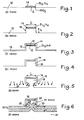
- FIGS. 1 to 6 represent the successive stages of the manufacturing process according to the invention.
- a substrate 10 which is a slice of monocrystalline silicon, which is uniformly covered, after formation of a thin layer of silicon oxide 12 (approximately 500 angstroms), of a layer of silicon nitride 14
- the oxide is simply intended to prevent the nitride layer from degrading the crystal quality of the silicon surface which it covers.
- the layers 14 and 12 are etched in a pattern leaving small-width flows remaining at the place where one would like islands of monocrystalline silicon isolated dielectrically from the substrate.
- This etching of the nitride is conventionally done after depositing a layer of resin, exposure through an appropriate mask, development of the resin, and chemical attack of the nitride where it is not protected by the resin. The result is shown in Figure 1.
- the monocrystalline silicon is attacked where it is not covered with nitride, according to a vertical anisotropic etching process (by CC1 4 plasma for example or by reactive ion etching), on a thickness h of around 0.5 micron.
- a vertical anisotropic etching process by CC1 4 plasma for example or by reactive ion etching
- streams 16 of monocrystalline silicon with substantially vertical sides, projecting above the surface of the wafer, these streams having a small width L and being covered with a layer of silicon nitride 14 (FIG. 2).
- a second layer 18 of nitride is then deposited, uniformly, so as to cover not only the surface of the wafer, but also the vertical sides and the upper surface of the islands; the latter is already covered with nitride, so that it has a nitride thickness greater than that which exists on the rest of the wafer surface at the end of the deposition (FIG. 3).
- An anisotropic etching is then carried out, substantially vertically, of the silicon nitride, by reactive ion etching or by etching with an anisotropic plasma (for example plasma of SF 6 , anisotropic for nitride).
- the etching is stopped when a vertical thickness of nitride equal to the thickness of the second layer has been eliminated, that is to say in practice when the silicon appears bare outside the waves 16.
- the etching can be stopped be done in particular by detecting, by optical or physical means (pressure change detection) the start of the attack on the exposed silicon. There then remains on the edge of the streams 16 of monocrystalline silicon covered on their sides with silicon nitride (in principle without interposition of silicon oxide) and covered on top with thin oxide and silicon nitride (FIG. 4).
- Isotropic etching of the silicon is then carried out where it is not protected by the nitride, for example by means of an SF 6 plasma (isotropic for the attack of silicon) or by a chemical bath.
- the duration and the attack conditions are chosen such that the silicon is dug to a depth p approximately equal to a quarter of the width L of the waves, for example 0.25 microns for a flow of 1 micron wide.
- a thick thermal oxidation of the silicon is carried out, so that the silicon is oxidized over its entire exposed surface, including under the overhanging edges of the waves, to a thickness such as the oxide layers 20 created on each side. of the width L of the stream meet in the center of the flow; a zone 22 of monocrystalline silicon, constituting the upper part of the flow 16, is thus completely isolated by the thick oxide 20 (FIG. 6).
- a thermal oxidation "consumes" a part of silicon thickness, (approximately half of the final oxide thickness), that is to say in practice, to fill the thickness L- 2d of monocrystalline silicon constituting the foot of the island in FIG. 5, it is necessary to grow an oxide thickness e approximately equal to L-2d over the entire surface of the wafer.
- Figure 6 there is shown in dotted lines the initially bare surface of the silicon to show that the oxide croft about as much outside as inside this surface.
- zone 22 of monocrystalline silicon it must have a minimum height z and that it is not completely invaded by the rise of the thick oxide. This therefore assumes that we started from a height h of initial silicon flux (fig 2) sufficiently high compared to the width L of the flux, for example from a height h equal to z + L-2d where z is the minimum height of monocrystalline silicon that we want to keep.
- a case is shown where we accept a smaller value of z (for example 0.25 micron) and a digging depth d greater than 1/4, for example 0.3 micron so that the height h can be substantially equal to half the width L.
- the last step not shown will consist in removing the nitride remaining on the top and the sides of the stream, after which the desired integrated circuit elements can be produced on the streams.
- the monocrystalline silicon thus dielectrically isolated from the substrate is of the same quality as the silicon of the substrate.
- Bipolar circuits like MOS circuits can be produced by this method.
- the structure produced makes it perfectly compatible to produce, on the same integrated circuit chip, elements dielectrically isolated from the substrate and elements that are not isolated or conventionally isolated by junction.
- the method described is particularly simple: it comprises only a small number of very conventional steps, with a single mask for defining the flows.
Landscapes
- Element Separation (AREA)
- Recrystallisation Techniques (AREA)
Applications Claiming Priority (2)
| Application Number | Priority Date | Filing Date | Title |
|---|---|---|---|
| FR8317584 | 1983-11-04 | ||
| FR8317584A FR2554638A1 (fr) | 1983-11-04 | 1983-11-04 | Procede de fabrication de structures integrees de silicium sur ilots isoles du substrat |
Publications (2)
| Publication Number | Publication Date |
|---|---|
| EP0146427A2 true EP0146427A2 (de) | 1985-06-26 |
| EP0146427A3 EP0146427A3 (de) | 1985-07-31 |
Family
ID=9293808
Family Applications (1)
| Application Number | Title | Priority Date | Filing Date |
|---|---|---|---|
| EP84402180A Withdrawn EP0146427A3 (de) | 1983-11-04 | 1984-10-30 | Verfahren zur Herstellung von integrierten Siliziumstrukturen auf isolierten Inseln eines Substrats |
Country Status (3)
| Country | Link |
|---|---|
| US (1) | US4561932A (de) |
| EP (1) | EP0146427A3 (de) |
| FR (1) | FR2554638A1 (de) |
Families Citing this family (22)
| Publication number | Priority date | Publication date | Assignee | Title |
|---|---|---|---|---|
| US4604162A (en) * | 1983-06-13 | 1986-08-05 | Ncr Corporation | Formation and planarization of silicon-on-insulator structures |
| JPS6072243A (ja) * | 1983-09-28 | 1985-04-24 | Matsushita Electric Ind Co Ltd | 半導体集積回路装置 |
| JPS61125039A (ja) * | 1984-11-21 | 1986-06-12 | Nec Corp | 半導体装置の製造方法 |
| US4764799A (en) * | 1985-05-28 | 1988-08-16 | International Business Machines Corporation | Stud-defined integrated circuit structure |
| US4648173A (en) * | 1985-05-28 | 1987-03-10 | International Business Machines Corporation | Fabrication of stud-defined integrated circuit structure |
| US5023690A (en) * | 1986-10-24 | 1991-06-11 | Texas Instruments Incorporated | Merged bipolar and complementary metal oxide semiconductor transistor device |
| US4753896A (en) * | 1986-11-21 | 1988-06-28 | Texas Instruments Incorporated | Sidewall channel stop process |
| US5346834A (en) * | 1988-11-21 | 1994-09-13 | Hitachi, Ltd. | Method for manufacturing a semiconductor device and a semiconductor memory device |
| JPH05121321A (ja) * | 1991-10-25 | 1993-05-18 | Rohm Co Ltd | シリコンの結晶成長法 |
| US5393375A (en) * | 1992-02-03 | 1995-02-28 | Cornell Research Foundation, Inc. | Process for fabricating submicron single crystal electromechanical structures |
| DE59402800D1 (de) * | 1993-04-05 | 1997-06-26 | Siemens Ag | Verfahren zur Herstellung von Tunneleffekt-Sensoren |
| TW309647B (de) * | 1995-12-30 | 1997-07-01 | Hyundai Electronics Ind | |
| US5841169A (en) * | 1996-06-27 | 1998-11-24 | Harris Corporation | Integrated circuit containing devices dielectrically isolated and junction isolated from a substrate |
| US5963789A (en) * | 1996-07-08 | 1999-10-05 | Kabushiki Kaisha Toshiba | Method for silicon island formation |
| US5691230A (en) * | 1996-09-04 | 1997-11-25 | Micron Technology, Inc. | Technique for producing small islands of silicon on insulator |
| US6211039B1 (en) * | 1996-11-12 | 2001-04-03 | Micron Technology, Inc. | Silicon-on-insulator islands and method for their formation |
| US6046477A (en) * | 1998-03-17 | 2000-04-04 | Micron Technology, Inc. | Dense SOI programmable logic array structure |
| US6215145B1 (en) | 1998-04-06 | 2001-04-10 | Micron Technology, Inc. | Dense SOI flash memory array structure |
| US6093623A (en) * | 1998-08-04 | 2000-07-25 | Micron Technology, Inc. | Methods for making silicon-on-insulator structures |
| DE10065895C1 (de) * | 2000-11-17 | 2002-05-23 | Infineon Technologies Ag | Elektronisches Bauteil mit Abschirmung und Verfahren zu seiner Herstellung |
| US6642090B1 (en) * | 2002-06-03 | 2003-11-04 | International Business Machines Corporation | Fin FET devices from bulk semiconductor and method for forming |
| US6753216B2 (en) * | 2002-10-31 | 2004-06-22 | Freescale Semiconductor, Inc. | Multiple gate transistor employing monocrystalline silicon walls |
Family Cites Families (6)
| Publication number | Priority date | Publication date | Assignee | Title |
|---|---|---|---|---|
| US4264382A (en) * | 1978-05-25 | 1981-04-28 | International Business Machines Corporation | Method for making a lateral PNP or NPN with a high gain utilizing reactive ion etching of buried high conductivity regions |
| JPS5743438A (en) * | 1980-08-29 | 1982-03-11 | Toshiba Corp | Semiconductor device and manufacture thereof |
| JPS5815427A (ja) * | 1981-07-20 | 1983-01-28 | 株式会社日立製作所 | 電池用電源回路 |
| JPS58132946A (ja) * | 1982-02-03 | 1983-08-08 | Toshiba Corp | 半導体装置の製造方法 |
| US4502913A (en) * | 1982-06-30 | 1985-03-05 | International Business Machines Corporation | Total dielectric isolation for integrated circuits |
| NL187373C (nl) * | 1982-10-08 | 1991-09-02 | Philips Nv | Werkwijze voor vervaardiging van een halfgeleiderinrichting. |
-
1983
- 1983-11-04 FR FR8317584A patent/FR2554638A1/fr active Pending
-
1984
- 1984-10-30 EP EP84402180A patent/EP0146427A3/de not_active Withdrawn
- 1984-11-02 US US06/667,587 patent/US4561932A/en not_active Expired - Fee Related
Also Published As
| Publication number | Publication date |
|---|---|
| EP0146427A3 (de) | 1985-07-31 |
| US4561932A (en) | 1985-12-31 |
| FR2554638A1 (fr) | 1985-05-10 |
Similar Documents
| Publication | Publication Date | Title |
|---|---|---|
| FR2554638A1 (fr) | Procede de fabrication de structures integrees de silicium sur ilots isoles du substrat | |
| EP1697975B1 (de) | Verfahren zum versiegeln zweier platten mit ausbildung eines ohmschen kontakts dazwischen | |
| EP0763849B1 (de) | Verfahren zur Herstellung dünner Halbleiterschichten | |
| EP1923912B1 (de) | Verfahren zur Herstellung einer gemischten mikrotechnologischen Struktur | |
| FR2812764A1 (fr) | Procede de fabrication d'un substrat de type substrat-sur- isolant ou substrat-sur-vide et dispositif obtenu | |
| JP2000243944A (ja) | シリコン・オン・インシュレータ構造およびその製造方法 | |
| EP0673062B1 (de) | Isolationsverfahren für aktive Zonen eines Halbleitersubstrates mit untiefen planarisierten Graben | |
| FR2813144A1 (fr) | Procede pour empecher la courbure de couches de semiconducteur et dispositif a semiconducteur forme par ce procede | |
| EP1111669A1 (de) | Verfahren zur Herstellung von isolierten metallischen Verbindungsleitungen in integrierten Schaltkreisen | |
| US8507332B2 (en) | Method for manufacturing components | |
| EP1638141B1 (de) | Verfahren zur Hestellung von zusammengestzten Halbleiterplättchen mittels Schichtübertragung | |
| FR2847382A1 (fr) | Realisation de tranchees fines et rapprochees | |
| EP1407486B1 (de) | Herstellungsverfahren für einen transistor auf einem soi-substrat | |
| FR3019937A1 (fr) | Procede de formation de tranchees d'isolement | |
| EP2690655A2 (de) | Verfahren zur Herstellung von Durchkontaktierungen | |
| FR2880191A1 (fr) | Realisation de tranchees ou puits ayant des destinations differentes dans un substrat semiconducteur | |
| JP2004047851A (ja) | 半導体装置の製造方法 | |
| EP2229689B1 (de) | Verfahren für lokalisierte heteroepitaxie auf einem dielektrikum, im besonderen von germanium auf oxidiertem silicium, sowie verfahren zur herstellung einer produktionsbasis einer homogenen oder heterogenen integrierten schaltung | |
| KR100511900B1 (ko) | 에스오아이 기판의 제조방법 | |
| KR100327571B1 (ko) | 반도체장치의 소자분리막 형성방법 | |
| FR3143841A1 (fr) | Procédé de préparation d’un empilement en vue d’un collage | |
| WO2025108884A1 (fr) | Procede de fabrication de super reseaux doubles obtenus par transfert de couche | |
| FR2791472A1 (fr) | Procede de creation de lignes de connexion et de points de contact sous-jacents dans un substrat dielectrique | |
| FR2853451A1 (fr) | Couches monocristallines heteroatomiques | |
| JPH0582526A (ja) | 半導体基板 |
Legal Events
| Date | Code | Title | Description |
|---|---|---|---|
| PUAI | Public reference made under article 153(3) epc to a published international application that has entered the european phase |
Free format text: ORIGINAL CODE: 0009012 |
|
| PUAL | Search report despatched |
Free format text: ORIGINAL CODE: 0009013 |
|
| AK | Designated contracting states |
Designated state(s): DE GB IT NL |
|
| AK | Designated contracting states |
Designated state(s): DE GB IT NL |
|
| 17P | Request for examination filed |
Effective date: 19860118 |
|
| STAA | Information on the status of an ep patent application or granted ep patent |
Free format text: STATUS: THE APPLICATION HAS BEEN WITHDRAWN |
|
| 17Q | First examination report despatched |
Effective date: 19870413 |
|
| 18W | Application withdrawn |
Withdrawal date: 19870421 |
|
| RIN1 | Information on inventor provided before grant (corrected) |
Inventor name: GRIS, YVON Inventor name: MONROY-AGUIRRE, AGUSTIN |