EP0148021A2 - Dispositif laser à semiconducteur - Google Patents
Dispositif laser à semiconducteur Download PDFInfo
- Publication number
- EP0148021A2 EP0148021A2 EP84309072A EP84309072A EP0148021A2 EP 0148021 A2 EP0148021 A2 EP 0148021A2 EP 84309072 A EP84309072 A EP 84309072A EP 84309072 A EP84309072 A EP 84309072A EP 0148021 A2 EP0148021 A2 EP 0148021A2
- Authority
- EP
- European Patent Office
- Prior art keywords
- layer
- refractive index
- coating layer
- clad
- semiconductor laser
- Prior art date
- Legal status (The legal status is an assumption and is not a legal conclusion. Google has not performed a legal analysis and makes no representation as to the accuracy of the status listed.)
- Granted
Links
- 239000004065 semiconductor Substances 0.000 title claims abstract description 31
- 239000010410 layer Substances 0.000 claims abstract description 155
- 239000011247 coating layer Substances 0.000 claims abstract description 58
- 239000000758 substrate Substances 0.000 claims abstract description 20
- 230000000063 preceeding effect Effects 0.000 claims 2
- 125000005842 heteroatom Chemical group 0.000 abstract description 13
- 230000000694 effects Effects 0.000 abstract description 10
- 238000010276 construction Methods 0.000 abstract description 5
- 238000000034 method Methods 0.000 description 15
- 230000008569 process Effects 0.000 description 15
- 229910001218 Gallium arsenide Inorganic materials 0.000 description 10
- 238000004519 manufacturing process Methods 0.000 description 8
- 239000013078 crystal Substances 0.000 description 7
- 238000002488 metal-organic chemical vapour deposition Methods 0.000 description 6
- 238000009826 distribution Methods 0.000 description 5
- 238000010521 absorption reaction Methods 0.000 description 4
- 239000000463 material Substances 0.000 description 4
- HQWPLXHWEZZGKY-UHFFFAOYSA-N diethylzinc Chemical compound CC[Zn]CC HQWPLXHWEZZGKY-UHFFFAOYSA-N 0.000 description 3
- 238000001451 molecular beam epitaxy Methods 0.000 description 3
- RBFQJDQYXXHULB-UHFFFAOYSA-N arsane Chemical compound [AsH3] RBFQJDQYXXHULB-UHFFFAOYSA-N 0.000 description 2
- 239000002019 doping agent Substances 0.000 description 2
- 238000005530 etching Methods 0.000 description 2
- 238000001764 infiltration Methods 0.000 description 2
- 230000008595 infiltration Effects 0.000 description 2
- 229910052751 metal Inorganic materials 0.000 description 2
- 239000002184 metal Substances 0.000 description 2
- 230000010355 oscillation Effects 0.000 description 2
- 230000009467 reduction Effects 0.000 description 2
- 239000011701 zinc Substances 0.000 description 2
- 229910017401 Au—Ge Inorganic materials 0.000 description 1
- BUGBHKTXTAQXES-UHFFFAOYSA-N Selenium Chemical compound [Se] BUGBHKTXTAQXES-UHFFFAOYSA-N 0.000 description 1
- 229910000070 arsenic hydride Inorganic materials 0.000 description 1
- 230000008901 benefit Effects 0.000 description 1
- 239000012159 carrier gas Substances 0.000 description 1
- 230000008859 change Effects 0.000 description 1
- 238000005229 chemical vapour deposition Methods 0.000 description 1
- 150000001875 compounds Chemical class 0.000 description 1
- 239000000835 fiber Substances 0.000 description 1
- 239000007789 gas Substances 0.000 description 1
- 238000002347 injection Methods 0.000 description 1
- 239000007924 injection Substances 0.000 description 1
- 239000007791 liquid phase Substances 0.000 description 1
- 238000013178 mathematical model Methods 0.000 description 1
- 230000003287 optical effect Effects 0.000 description 1
- 229920002120 photoresistant polymer Polymers 0.000 description 1
- 239000002994 raw material Substances 0.000 description 1
- 238000003892 spreading Methods 0.000 description 1
- 230000007480 spreading Effects 0.000 description 1
- JLTRXTDYQLMHGR-UHFFFAOYSA-N trimethylaluminium Chemical compound C[Al](C)C JLTRXTDYQLMHGR-UHFFFAOYSA-N 0.000 description 1
- XCZXGTMEAKBVPV-UHFFFAOYSA-N trimethylgallium Chemical compound C[Ga](C)C XCZXGTMEAKBVPV-UHFFFAOYSA-N 0.000 description 1
- 238000005406 washing Methods 0.000 description 1
Images


Classifications
-
- H—ELECTRICITY
- H01—ELECTRIC ELEMENTS
- H01S—DEVICES USING THE PROCESS OF LIGHT AMPLIFICATION BY STIMULATED EMISSION OF RADIATION [LASER] TO AMPLIFY OR GENERATE LIGHT; DEVICES USING STIMULATED EMISSION OF ELECTROMAGNETIC RADIATION IN WAVE RANGES OTHER THAN OPTICAL
- H01S5/00—Semiconductor lasers
- H01S5/20—Structure or shape of the semiconductor body to guide the optical wave ; Confining structures perpendicular to the optical axis, e.g. index or gain guiding, stripe geometry, broad area lasers, gain tailoring, transverse or lateral reflectors, special cladding structures, MQW barrier reflection layers
- H01S5/22—Structure or shape of the semiconductor body to guide the optical wave ; Confining structures perpendicular to the optical axis, e.g. index or gain guiding, stripe geometry, broad area lasers, gain tailoring, transverse or lateral reflectors, special cladding structures, MQW barrier reflection layers having a ridge or stripe structure
- H01S5/223—Buried stripe structure
- H01S5/2231—Buried stripe structure with inner confining structure only between the active layer and the upper electrode
-
- H—ELECTRICITY
- H01—ELECTRIC ELEMENTS
- H01S—DEVICES USING THE PROCESS OF LIGHT AMPLIFICATION BY STIMULATED EMISSION OF RADIATION [LASER] TO AMPLIFY OR GENERATE LIGHT; DEVICES USING STIMULATED EMISSION OF ELECTROMAGNETIC RADIATION IN WAVE RANGES OTHER THAN OPTICAL
- H01S5/00—Semiconductor lasers
- H01S5/20—Structure or shape of the semiconductor body to guide the optical wave ; Confining structures perpendicular to the optical axis, e.g. index or gain guiding, stripe geometry, broad area lasers, gain tailoring, transverse or lateral reflectors, special cladding structures, MQW barrier reflection layers
- H01S5/22—Structure or shape of the semiconductor body to guide the optical wave ; Confining structures perpendicular to the optical axis, e.g. index or gain guiding, stripe geometry, broad area lasers, gain tailoring, transverse or lateral reflectors, special cladding structures, MQW barrier reflection layers having a ridge or stripe structure
- H01S5/2205—Structure or shape of the semiconductor body to guide the optical wave ; Confining structures perpendicular to the optical axis, e.g. index or gain guiding, stripe geometry, broad area lasers, gain tailoring, transverse or lateral reflectors, special cladding structures, MQW barrier reflection layers having a ridge or stripe structure comprising special burying or current confinement layers
- H01S5/2206—Structure or shape of the semiconductor body to guide the optical wave ; Confining structures perpendicular to the optical axis, e.g. index or gain guiding, stripe geometry, broad area lasers, gain tailoring, transverse or lateral reflectors, special cladding structures, MQW barrier reflection layers having a ridge or stripe structure comprising special burying or current confinement layers based on III-V materials
-
- H—ELECTRICITY
- H01—ELECTRIC ELEMENTS
- H01S—DEVICES USING THE PROCESS OF LIGHT AMPLIFICATION BY STIMULATED EMISSION OF RADIATION [LASER] TO AMPLIFY OR GENERATE LIGHT; DEVICES USING STIMULATED EMISSION OF ELECTROMAGNETIC RADIATION IN WAVE RANGES OTHER THAN OPTICAL
- H01S5/00—Semiconductor lasers
- H01S5/30—Structure or shape of the active region; Materials used for the active region
- H01S5/32—Structure or shape of the active region; Materials used for the active region comprising PN junctions, e.g. hetero- or double- heterostructures
- H01S5/323—Structure or shape of the active region; Materials used for the active region comprising PN junctions, e.g. hetero- or double- heterostructures in AIIIBV compounds, e.g. AlGaAs-laser, InP-based laser
- H01S5/32308—Structure or shape of the active region; Materials used for the active region comprising PN junctions, e.g. hetero- or double- heterostructures in AIIIBV compounds, e.g. AlGaAs-laser, InP-based laser emitting light at a wavelength less than 900 nm
- H01S5/32316—Structure or shape of the active region; Materials used for the active region comprising PN junctions, e.g. hetero- or double- heterostructures in AIIIBV compounds, e.g. AlGaAs-laser, InP-based laser emitting light at a wavelength less than 900 nm comprising only (Al)GaAs
Definitions
- This invention relates generally to the field of lasers, and more particularly, is directed to a semiconductor laser device having a current confinement structure and a built-in waveguide structure.
- LPE liquid phase epitaxial process
- MBE molecular beam epitaxy
- MOCVD metalorganic chemical vapor deposition
- a semiconductor laser -having a suitable construction for manufacture by the MOCVD process is disclosed in Applied Physics Letters, Vol. 37, No. 3, p. 262 and is illustrated in Figure 1.
- current confining layer 5 which confines the current to the direction parallel to the junction plane and controls the transverse mode of the laser, is provided in upper clad layer 4 formed on flat active layer 3.
- the active layer 3 is formed from a different conductive type material than neighboring p-type clad layer 4 and p-type coating layer 6. Thus, no current flow passes through layer 5.
- Active layer 3 is formed on an n-GaAs substrate through an n-GaAlAs clad layer 2 and p - GaAlAs clad layer 4 is covered with a p-GaAs contact layer. Further, the p-GaAs contact layer 7 and the n-GaAs substrate have a pair of metal electrodes 8 and 9, respectively.
- This type of laser device produces both a current confinement effect in the horizontal direction of the junction plane by confining the current in layer 5 and a built in refraction index waveguide effect.
- a low threshold of around 50 mA, is achieved with room temperature pulse oscillation and that single mode oscillation is achievable so that the transverse mode can be controlled satisfactorily.
- BH Buried hetero structures
- TJS transverse junction stripe structures
- the threshold value of a laser with the construction shown in Figure 1 is 50 mA which is more than double the value for lasers with BH and TJS structures. Tests conducted by the inventors showed that with present structures, it is difficult to reduce the threshold value. The reason for the difference between the laser illustrated in Figure 1 and lasers having a BH or TJS structure is probably due to differences in the waveguide effects in the structures.
- the threshold value is probably increased by an amount corresponding to the absorption loss in the structure shown in Figure 1.
- FIG. 2 A semiconductor laser of this type is shown in Figure 2.
- This device basically includes the same layers as in the device shown in Figure 1, however, clad layer -4 is thick enough not to infiltrate light to current confining layer 5 which has a high refractive index and absorbs lights.
- Figure 3 illustrates calculated curves indicating the relationship between effective refractive index Neff of the lowest waveguide mode in the light waveguide path and refractive index Nc of the higher refractive layer provided at one side of the light waveguide path in the typical double - hetero structure laser. This mathematical model corresponds to the portion of the structure just beneath the stripe of the laser shown in Figure 2.
- Figure 3 also indicates that the increase of the effective refractive index depends on the thickness of clad layer 4. The smaller the thickness, the larger the increase in effective refractive index.
- the ⁇ Neff should be larger than 10- 3 in order to stabilized control of the traverse mode in the horizontal direction of the junction plane.
- the lasing threshold value is higher than expected due to the following problems.
- the first problem is that the lasing threshhold is apt to become the condition of cutoff because of variations in the thickness and refractive index in active layer 3, clad layer 4 and coating layer 6.
- Another problem is that the cut off condition of the waveguide mode depends upon the thickness of clad layer 4. Thus, the waveguide mode often becomes cut off where thickness h is larger even if there exists a waveguide mode where thickness h is smaller.
- the sides of the stripe corresponds to the portion wherein thickness h of clad layer 4 becomes substantially larger and thus it becomes a cutoff condition for the waveguide mode.
- This phenomenon is also made clear by the fact that radiant brightnesses appear at the sides of the stripe on top of the active layer. This fact is revealed in infrared microscope examination of this type of laser.
- the threshold current is expected to be lower than in a laser with the structure of Figure 1 due to the change from a loss waveguide structure to a refraction index waveguide structure.
- a semiconductor laser comprising: a substrate; a first clad layer of a first conductive type formed on the substrate; an active layer on the first clad layer; a second clad layer of a second conductive type formed on the active layer; a first current confining layer of said first conductive type formed on the second clad layer, and divided into two parts; a first coating layer of the second conductive type formed on the current confining layer and in the divide between the two parts of the current confining layer, the first coating layer having a refractive index larger than the refractive index of the second clad layer; a second coating layer of the second conductive type formed on the first coating layer with a refractive index smaller than the refractive index of the first coating layer; and a pair of electrodes overlying at least part of and electrically connected to the second coating layer and the substrate respectively.
- a hetero junction type semiconductor laser device having current confining and built-in 4"waveguide effects.
- a hetero junction layer of a different conduction type than the clad layer is formed on the clad layer with a stripe shape groove portion and a coating layer of the same conductive type as the clad layer is formed on top of this.
- the coating layer is formed from at least two layers.
- a first coating layer, which is nearer the active layer, has a refractive index greater than that of the clad layer.
- a second coating layer which is further away from the active layer than the first coating layer, has a refrective index that is smaller than that of the first coating layer.
- the embedded layer in the stripe shape groove portion of the present invention is formed of at least two layers comprising a high refractive index layer and a low refractive index layer, light infiltrating into the stripe groove portion is affected by the high refractive layer so that the effective refractive index distribution in the horizontal direction at the junction plane is maximum at the stripe shape groove portion. Also, the effect of the existing low refractive index layer outside of the high refractive index layer prevents cutoff of the waveguide mode and has a large effective refractive index distribution even when the distance between the first coating layer and the active layer is large or where a higher refractive index is selected for the first coating layer.
- Figure 4 is a cross-sectional view showing, the general construction of a semiconductor laser according to one embodiment of the present invention.
- 21 is an N - GaAs substrate
- 22 an N - Gap 0.65 Al 0.35 As clad layer
- 23 a G 0.92 Al 0.08 As active layer
- 24 a P - Ga 0.65 Al 0.35 As clad layer
- 25 an N - GaAs current confining layer (hetero layer)
- 26 a P - Ga 0.8 AI 0.2 As first coating layer
- 27 a P - Ga 0.65 Al 0.3 As second coating layer
- 28 a P - GaAs contact layer.
- Elements 29 and 30 are metal electrode layers.
- a laser with the above construction is produced by the stages shown in Figures 5A - 5C.
- N - Ga 0.65 Al 0.35 As clad layer 22 1.5 jum thick, (Se doping, 1 x 10 17 cm -3 ), undoped Ga 0.92 AI 0.08 As active layer 23 0.08 pm thick, p - Ga 0.65 AI 0.35 AS clad layer 24 1.5 ⁇ m thick (Zn doping, 7 x 10 18 cm -3 ) and N - GaAs current confining layer (hetero layer) 1 ⁇ m thick (Se doping, 5 x 10 18 cm -3 ) are successively grown on substrate 21 (Si doping, 1 x 10 18 cm -3 ).
- MOCVD is used in this first crystal growth stage.
- the raw materials used are trimethyl gallium (TMG: (CH) 3 Ga), trimethyl aluminium (TMA : (CH 3 ) 3 AI), arsine (AsH 3 ), diethyl zinc (DEZ : (C 2 H 5 ) 2 Zn) as a p-dopant and hydrogen selenide (H 2 Se) as and n-dopant.
- the growth rate is 0.25 pm/min. It is not absolutely necessary to use the MOCVD process in the first crystal growth stage but where mass production is desired, the MOCVO process permits crystal growth with good uniformity over a large surface area and thus is more advantageous than the LPE process.
- photoresist 31 is coated on current confining layer 25.
- Resist 31 defines a stripe-shaped window 3 um wide and serves as a mask in selective etching of current confining layer 25.
- An etching process in then used to form stripe-shaped groove 32.
- a second crystal growth stage is effected by the MOCVD process.
- a 0.03 ⁇ m thick p - Ga 0.8 Al 0.2 As first coating layer 26, P - Ga 0.65 Al 0.35 As second coating layer 27 and P - GaAs coating layer 28 (Zn doping, 5 x 10 8 cm- 3 ) are grown and formed over the whole surface as shown in Figure 5C.
- a Cr-Au electrode 29 is attached to the top of contact layer 28 and an Au-Ge electrode 30 is attached to the lower surface of substrate 21 by a normal electrode attachment process.
- the refractive indices of the above embodiment are 3.59 in active layer 23, 3.385 in clad layers 22, 24, 3.45 in first coating layer 26 and 3.385 in second coating layer 27.
- the operating characteristics of a laser formed from the above structure with a resonator length of 250 pm were found to be excellent.
- the threshold current was low at about 35 mA and the differential quantum efficiency was high at about 50%.
- a current - light output characteristic with good linearity was achieved with no kinks up to an output of 12 mW or more.
- the effective refractive index of the mode must be an intermediate value between the highest refractive index among all the layers forming the waveguide path and the higher refractive index of the outer most layers forming the waveguide path. If the effective refractive index is smaller than that of the outer most higher refractive index layer of the waveguide path, light is directed to the outside of the waveguide path so that no waveguide mode can exist.
- the waveguide mode can exist.
- a waveguide path having an asymmetrical distribution of refractive indices such as shown in Fig. 2
- no waveguide mode can exist even though the above condition of effective refractive index is satisfied.
- Such a cutoff of the waveguide mode easily occurs in double hetero structure lasers having a rather thin active layer and where the effective refractive index of the waveguide is close to the refractive index of the clad layer.
- the waveguide mode is apt to be cut off when there is a difference in refractive indices of both clad layers or when a higher refractive layer is provided close to one of the clad layers as shown in Fig. 2.
- This problem can be overcome by providing a lower refractive index layer (second coating layer) outside of the high refractive index layer (first coating layer).
- the lower refractive index layer refracts light which might be dispensed outside of the higher refractive index layer when there is no lower refractive index layer.
- the waveguide mode can be formed.
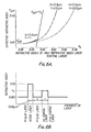
- Figure 6A shows operating characteristic curves of the refractive index Neff when the refractive index Nc of high refractive index layer is changed when there is a lower refractive index layer.
- Figure 6B shows parameters for deriving the curves of Figure 6A.
- the thickness of the active layer is 0.08 ⁇ m
- h indicates the thickness of clad layer 24
- t indicates the thickness of the high refractive index layer, i.e., first coating layer 26.
- the refractive index of the second coating layer is equal to that of the clad layer in calculating the curves shown in Figure 6A. In this situation, cut off may not occur. It is noted, however, that this situation is not always necessary. When the refractive index of the second coating layer is different from that of the clad layer, cut off may occur at a very high value of the effective refractive index compared to the condition in which the second coating layer is not provided. Thus, the increment 6 Neff can be easily realized at 10- 3- 10- 2 according to the present invention. Also, cut off does not occur at the sides of the stripe shape groove portion so that threshold current can be maintained low to achieve a lower threshold value.
- FIG. 7 is a cross-sectional view showing the general structure of a semiconductor laser according to another embodiment of the invention. Parts that are the same as in Figure 4 are identified by the same numbers and a detailed description thereof will be omitted.
- the hetero layer is made of two layers. That is, n - Ga 0.4 Al 0.6
- second hetero layer 25a is inserted between p - GaAlAs clad layer 24 and n - GaAs first hetero layer 25. This contributes to producing a smaller effective refractive index for the mode guided by active Jayer 23 in the region on opposite sides of the stripe.
- first coating layer 26 it is also possible to produce a large effective index distribution immediately below the stripe.
- An advantage of the introduction of the second hetero layer 25a is that the reactive current component that spreads through p - clad layer 24 in the embodiment of Figure 4 is reduced by an amount corresponding to the reduction of the thickness of p - clad layer 24.
- the structural material is not limited to being GaAIAs but other compound semiconductor materials may be used such as InGaAsP or AIGaInP, etc.
- the MBE process may be used instead of the MOCVD process.
Landscapes
- Physics & Mathematics (AREA)
- Geometry (AREA)
- Condensed Matter Physics & Semiconductors (AREA)
- General Physics & Mathematics (AREA)
- Electromagnetism (AREA)
- Optics & Photonics (AREA)
- Semiconductor Lasers (AREA)
Applications Claiming Priority (2)
| Application Number | Priority Date | Filing Date | Title |
|---|---|---|---|
| JP58246148A JPH067618B2 (ja) | 1983-12-26 | 1983-12-26 | 半導体レ−ザ装置 |
| JP246148/83 | 1983-12-26 |
Publications (3)
| Publication Number | Publication Date |
|---|---|
| EP0148021A2 true EP0148021A2 (fr) | 1985-07-10 |
| EP0148021A3 EP0148021A3 (en) | 1987-06-16 |
| EP0148021B1 EP0148021B1 (fr) | 1992-03-04 |
Family
ID=17144197
Family Applications (1)
| Application Number | Title | Priority Date | Filing Date |
|---|---|---|---|
| EP84309072A Expired EP0148021B1 (fr) | 1983-12-26 | 1984-12-21 | Dispositif laser à semiconducteur |
Country Status (4)
| Country | Link |
|---|---|
| US (1) | US4691321A (fr) |
| EP (1) | EP0148021B1 (fr) |
| JP (1) | JPH067618B2 (fr) |
| DE (1) | DE3485537D1 (fr) |
Cited By (1)
| Publication number | Priority date | Publication date | Assignee | Title |
|---|---|---|---|---|
| EP0214534A3 (fr) * | 1985-08-23 | 1988-04-20 | Kabushiki Kaisha Toshiba | Diode laser à semi-conducteur à mode transversal stabilisé comportant une couche de couplage constituant un guide d'onde |
Families Citing this family (9)
| Publication number | Priority date | Publication date | Assignee | Title |
|---|---|---|---|---|
| US5136601A (en) * | 1984-11-19 | 1992-08-04 | Hitachi, Ltd. | Semiconductor laser |
| JPS63166285A (ja) * | 1986-12-26 | 1988-07-09 | Toshiba Corp | 半導体発光装置の製造方法 |
| JP3116675B2 (ja) * | 1993-07-28 | 2000-12-11 | ソニー株式会社 | 半導体レーザー |
| JP3510305B2 (ja) * | 1994-02-22 | 2004-03-29 | 三菱電機株式会社 | 半導体レーザの製造方法,及び半導体レーザ |
| JP3897186B2 (ja) * | 1997-03-27 | 2007-03-22 | シャープ株式会社 | 化合物半導体レーザ |
| JP2000031600A (ja) * | 1998-07-14 | 2000-01-28 | Nec Corp | 半導体レーザの製造方法 |
| US6928223B2 (en) * | 2000-07-14 | 2005-08-09 | Massachusetts Institute Of Technology | Stab-coupled optical waveguide laser and amplifier |
| KR20060038057A (ko) * | 2004-10-29 | 2006-05-03 | 삼성전기주식회사 | 반도체 레이저 소자 및 그 제조 방법 |
| JP6753526B2 (ja) * | 2017-05-29 | 2020-09-09 | 三菱電機株式会社 | 半導体装置および半導体装置の製造方法 |
Family Cites Families (3)
| Publication number | Priority date | Publication date | Assignee | Title |
|---|---|---|---|---|
| GB1603643A (en) * | 1978-03-06 | 1981-11-25 | Coulter Electronics | Detection of blood disorders |
| JPS575070A (en) * | 1980-06-11 | 1982-01-11 | Toshiba Corp | Fixing device |
| GB2105099B (en) * | 1981-07-02 | 1985-06-12 | Standard Telephones Cables Ltd | Injection laser |
-
1983
- 1983-12-26 JP JP58246148A patent/JPH067618B2/ja not_active Expired - Lifetime
-
1984
- 1984-12-21 DE DE8484309072T patent/DE3485537D1/de not_active Expired - Lifetime
- 1984-12-21 EP EP84309072A patent/EP0148021B1/fr not_active Expired
- 1984-12-26 US US06/686,478 patent/US4691321A/en not_active Expired - Lifetime
Cited By (2)
| Publication number | Priority date | Publication date | Assignee | Title |
|---|---|---|---|---|
| EP0214534A3 (fr) * | 1985-08-23 | 1988-04-20 | Kabushiki Kaisha Toshiba | Diode laser à semi-conducteur à mode transversal stabilisé comportant une couche de couplage constituant un guide d'onde |
| US4799228A (en) * | 1985-08-23 | 1989-01-17 | Kabushiki Kaisha Toshiba | Transverse-mode stabilized semiconductor laser diode with slab-coupled waveguide |
Also Published As
| Publication number | Publication date |
|---|---|
| JPH067618B2 (ja) | 1994-01-26 |
| EP0148021A3 (en) | 1987-06-16 |
| JPS60137085A (ja) | 1985-07-20 |
| DE3485537D1 (de) | 1992-04-09 |
| EP0148021B1 (fr) | 1992-03-04 |
| US4691321A (en) | 1987-09-01 |
Similar Documents
| Publication | Publication Date | Title |
|---|---|---|
| CA1158754A (fr) | Laser a structure mesa canalisee | |
| US4635268A (en) | Semiconductor laser device having a double heterojunction structure | |
| US4371966A (en) | Heterostructure lasers with combination active strip and passive waveguide strip | |
| US7016391B2 (en) | Gain-coupled distributed feedback semiconductor laser device and production method therefor | |
| EP0148021B1 (fr) | Dispositif laser à semiconducteur | |
| US5084892A (en) | Wide gain region laser diode | |
| US5776792A (en) | Method for forming semiconductor laser device | |
| KR900000075B1 (ko) | 반도체레이저 다이오드 | |
| US4365336A (en) | Terraced substrate semiconductor laser | |
| JPH0518473B2 (fr) | ||
| US4447905A (en) | Current confinement in semiconductor light emitting devices | |
| US4983541A (en) | Semiconductor laser device fabrication | |
| US4677633A (en) | Semiconductor laser with a two-striped channel | |
| Yoshikawa et al. | A novel technology for formation of a narrow active layer in buried heterostructure lasers by single-step MOCVD | |
| JPS603178A (ja) | 半導体レ−ザ装置 | |
| JPS6246584A (ja) | 半導体レ−ザ装置 | |
| JPH0568873B2 (fr) | ||
| US4432092A (en) | Semiconductor laser | |
| US4358850A (en) | Terraced substrate semiconductor laser | |
| JPS621290A (ja) | ヘテロ接合型半導体レ−ザ | |
| JPH0574957B2 (fr) | ||
| JP3277711B2 (ja) | 半導体レーザ及びその製造方法 | |
| JP2973215B2 (ja) | 半導体レーザ装置 | |
| JPS59171187A (ja) | 半導体レ−ザ装置 | |
| JP2558767B2 (ja) | 半導体レーザ装置 |
Legal Events
| Date | Code | Title | Description |
|---|---|---|---|
| PUAI | Public reference made under article 153(3) epc to a published international application that has entered the european phase |
Free format text: ORIGINAL CODE: 0009012 |
|
| 17P | Request for examination filed |
Effective date: 19841221 |
|
| AK | Designated contracting states |
Designated state(s): DE FR GB |
|
| PUAL | Search report despatched |
Free format text: ORIGINAL CODE: 0009013 |
|
| AK | Designated contracting states |
Kind code of ref document: A3 Designated state(s): DE FR GB |
|
| 17Q | First examination report despatched |
Effective date: 19890711 |
|
| GRAA | (expected) grant |
Free format text: ORIGINAL CODE: 0009210 |
|
| AK | Designated contracting states |
Kind code of ref document: B1 Designated state(s): DE FR GB |
|
| ET | Fr: translation filed | ||
| REF | Corresponds to: |
Ref document number: 3485537 Country of ref document: DE Date of ref document: 19920409 |
|
| PLBE | No opposition filed within time limit |
Free format text: ORIGINAL CODE: 0009261 |
|
| STAA | Information on the status of an ep patent application or granted ep patent |
Free format text: STATUS: NO OPPOSITION FILED WITHIN TIME LIMIT |
|
| 26N | No opposition filed | ||
| PGFP | Annual fee paid to national office [announced via postgrant information from national office to epo] |
Ref country code: FR Payment date: 19971209 Year of fee payment: 14 |
|
| PGFP | Annual fee paid to national office [announced via postgrant information from national office to epo] |
Ref country code: GB Payment date: 19971212 Year of fee payment: 14 |
|
| PGFP | Annual fee paid to national office [announced via postgrant information from national office to epo] |
Ref country code: DE Payment date: 19971230 Year of fee payment: 14 |
|
| PG25 | Lapsed in a contracting state [announced via postgrant information from national office to epo] |
Ref country code: GB Free format text: LAPSE BECAUSE OF NON-PAYMENT OF DUE FEES Effective date: 19981221 |
|
| GBPC | Gb: european patent ceased through non-payment of renewal fee |
Effective date: 19981221 |
|
| PG25 | Lapsed in a contracting state [announced via postgrant information from national office to epo] |
Ref country code: FR Free format text: LAPSE BECAUSE OF NON-PAYMENT OF DUE FEES Effective date: 19990831 |
|
| REG | Reference to a national code |
Ref country code: FR Ref legal event code: ST |
|
| PG25 | Lapsed in a contracting state [announced via postgrant information from national office to epo] |
Ref country code: DE Free format text: LAPSE BECAUSE OF NON-PAYMENT OF DUE FEES Effective date: 19991001 |