EP0148164A2 - Umsetzer für ein Bildverarbeitungssystem - Google Patents
Umsetzer für ein Bildverarbeitungssystem Download PDFInfo
- Publication number
- EP0148164A2 EP0148164A2 EP85300077A EP85300077A EP0148164A2 EP 0148164 A2 EP0148164 A2 EP 0148164A2 EP 85300077 A EP85300077 A EP 85300077A EP 85300077 A EP85300077 A EP 85300077A EP 0148164 A2 EP0148164 A2 EP 0148164A2
- Authority
- EP
- European Patent Office
- Prior art keywords
- line
- input
- analog
- square
- output
- Prior art date
- Legal status (The legal status is an assumption and is not a legal conclusion. Google has not performed a legal analysis and makes no representation as to the accuracy of the status listed.)
- Withdrawn
Links
Images


Classifications
-
- H—ELECTRICITY
- H04—ELECTRIC COMMUNICATION TECHNIQUE
- H04N—PICTORIAL COMMUNICATION, e.g. TELEVISION
- H04N3/00—Scanning details of television systems; Combination thereof with generation of supply voltages
- H04N3/10—Scanning details of television systems; Combination thereof with generation of supply voltages by means not exclusively optical-mechanical
- H04N3/16—Scanning details of television systems; Combination thereof with generation of supply voltages by means not exclusively optical-mechanical by deflecting electron beam in cathode-ray tube, e.g. scanning corrections
- H04N3/22—Circuits for controlling dimensions, shape or centering of picture on screen
Definitions
- This invention relates to digital image processing, in general, and more particularly, to an improved method and apparatus for interfacing a digital image processor with an analog video input and output.
- the present invention provides apparatus which performs the functions of converting from rectangular to square format and back again and of doing necessary frequency corwerting.
- the digitizer of the present invention includes logic circuits which can key one of two oscillators to cause an analog-to-digital converter to convert at either a 10MHz rate or a 13MHz rate.
- the 10MHz rate corresponds to the rate necessary to scan a square aspect ratio signal
- the 13MHz which is approximately 4/3 of the 10MHz rate, used to convert a 4:3 aspect ratio signal.
- a number of pixels corresponding to the number of lines can be scanned in over the time required to scan that number in a square aspect ratio input, the pixels being those in a square at the center of the raster.
- the information read in at one of these rates is coupled through a buffer memory with data read in in bursts and read out at a constant system rate reduced still further to 8.33MHz for further processing.
- the basic system frequency to be 10MHz
- the 8.33MHz processing frequency is possible because of the time during blanking when retrace takes place on the raster.
- Converting back into an analog video signal is done much in the same manner.
- the processed information at a system frequency of, for example, 10MHz is read into another buffer memory and then read out of this buffer memory at the accelerated frequency of 13MHz, again, in bursts with the time between bursts corresponding to blanking and retrace.
- a separate RS-170 timing generator generates the necessary sync and blanking signals based on divided outputs from a 10MHz oscillator.
- pixel and line counters and end-of-line and end-of-field detectors are utilized in controlling reading and writing into the system.
- the basic purpose of the digitizer and digitizer interface is to take information in analog format from a television camera or to take information from another source or a test pattern and get into a form in which it can be processed by the frame processors, i.e., to get it at the proper frequency and with the proper synchronization signals.
- the other end of the digitizer interface system takes the processed data which is being input to the digitizer at the system frequency of 8.33 MHZ and converts it into the necessary output frequency of 13 MHZ to display on the conventional T.V. display which has a 4:3 aspect ratio.
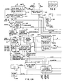
- FIG. 1 is a block diagram of the digitizer.
- an analog-to-digital converter 201 receiving a video input on line 203 from either an interlaced camera or a sequential scan camera.
- An input on line 205 is an encode command to the converter and an output on line 207 a data-ready output.
- a data output of 10 bits of data is provided on a data bus 209.
- the converter may be an Analog Devices Model 1020 for example.
- the digitizer also includes a sync recovery circuit.
- the video signal assuming that an interlaced scan with composite sync in the video signal is provided, is coupled into a sync recovery circuit 211 of conventional design where the sync is separated out from the video to provide a composite sync signal on line 213.
- This composite sync signal is coupled to a pulse shaping and regeneration'circuit 215 made up, primarily, of a group of monostable multivibrators from which three signals are provided as outputs.
- the first is the composite sync which will include both a vertical and horizontal sync information, a signal labeled CFS on line 219 which is the frame sync and a signal designated CIN which is a short pulse occurring at the field-time, i.e, occurring at the division between odd and even fields.
- a sequential scan camera provides as outputs a frame sync signal which is an input on line 221, a line sync signal which is an input on line 223 and a frame index signal which is an input on line 225.
- Lines 221 and 223 are clamped by zener diodes 227 and 229, respectively.
- Each of the three lines is coupled into a line receiver and driver 231 having uninverted and inverted outputs.
- a multiplexer 233 is provided to select betweeen either the recovered sync from the pulse shaping and regeneration circuit in the case of interlaced scan or incoming signals on lines 221, 223 and 225 in the case of sequential scan.
- the inverted index signal and the inverted CIN signal are provided to one set of inputs.
- Tne frame sync signal and CFS signal are provided to another set of signals inputs.
- the composite sync and line sync are provided to a third set of inputs and the index signal-and not inverted CN signal to the fourth set of inputs.
- One of the two sets of inputs is selected in accordance with a command labeled "composite" on line 235.
- this signal When composite video is present, i.e., when interlaced scan is being used, this signal will cause the outputs of pulse shaping and regeneration circuit 215 to be used. Where a sequential scan camera is used, it will cause the signals on lines 221, 223 and 225 to be used. These signals are provided as outputs through line drivers 237 to the remainder of the system.
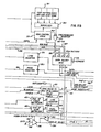
- FIG. 2 is a block diagram of the digitizer interface. This interface'is actually more than a digitizer interface. It interfaces the system riot only with the digitizer but with an output real time output monitor provides test patterns and generates various types of control and synchronization signals for use throughout the system. It also does various types of input and output conversions and provides the output to the display through a digital-to-analog converter. Also included in this section of the system and used therein are DMA, i.e., Direct Memory Access, inputs from the host processor which configure the system and set it up for the type of operation desired.
- DMA Direct Memory Access
- Block 301 is a sync- pulse to end of blanking delay counter.
- Block 303 is analog-to-digital converter control logic.
- A-D control logic 303 receives as one input the data-ready signal of the line 207.
- Adjacent line 207, bus 209, to which a signal from the logic circuit 303 is added, is visible.
- Adjacent that, the "composite" output which controls the multiplexer 233 of Figure 4, on line 235 is visible. Directly below that line is the encode line 205 discussed above in connection with Figure 4.
- the "composite" signal on line 235 is obtained from a control register 305 which receives an input from the DMA bus.
- control register When the control register is selected, by the signal labeled FNLT-4L, the values on the DMA bus are stored in the control register providing control information. On the other hand, when signal FNLT3L is present information is loaded into the address register. This includes the words, "Incount” and “outcount” "In count” indicates when it is time to begin inputing to the system, i.e., to begin using the input on bus 209 and processing it.
- the encode signal consists of a pulse train having either a frequency of 13MHz obtained from an oscillator 317 or 10MHz obtained from an oscillator 319. Which of the two rates are provided on the line 205 is determined by the input designated "Noninter" on a line 321 to a rate select multiplexer 323. The reason for this is that, as explained above, if noninterlaced information is being provided, it is in a 512 X 512 pixel format, i.e., it has a 1:1 aspect ratio. The normal interlaced scan, however, has a 4:3 aspect ratio.
- the input-rate must be accellerated by a ratio of 4/3 or to 13MHz.
- delay counter 301 must delay until the 85th pixel is reached as described above.
- the data from the analog-to-digital converter is provided as an input to a data select multiplexer 325.
- the data select multiplexer can select data from four separate inputs.
- One input, bus 209 is coupled to the analog-to-digital converter and a second 327 is coupled to a spare external input 329.
- Third and fourth buses are coupled to RAM control logic 331 and an exclusive OR gate checker board inverter 333. Which of the inputs is selected is determined by a two bit control signal from control register 305 called "mode" which is provided as an input to the multiplexer 325 on line 335.
- the "mode" input of line 335 is also an input to a sync-select multiplexer 337 at the left-hand side of the Figure.
- the sync-select multiplexer has four, three line inputs. These are, respectively, a noninterlace RAM input, an analog-to-digital input, a spare external input and an interlace RAM input.
- the outputs which are provided as inputs are the outputs from drivers 237 described in connection with Figure 4.
- Tne 10MHz oscillator 319 and 13MHz oscillator 317 are controlled by an output from clock control logic 339 on line 341. This determines when these keyed oscillators are turned on and turned off to read in data. Which of these is selected will, of course, be determined by whether or not there is a interlaced or noninterlaced input.
- the noninterlaced control signal from control register 305 is provided on a line 341 into an odd/even logic block 343 where it is combined with a first output of the sync-select multiplexer, the output corresponding to the index signal or representing field switchover.
- the field sync and line sync are provided as inputs to a block 345 labeled "delay from field sync to first valid line.”
- Tnis is a delay which is controlled by additional control signals from control register 305 on lines 347, 348 and 349 labeled "delay start,” “field zero delay” and “field one delay,” the last two representing the odd-and-even or even-and-odd field delays, respectively.
- These are delays which are programmable through the host processor and the control register, each having four bits of data to take into account system delays.
- an output signal is provided to clock- control logic 339 on line 350.
- an output of the control logic 303 on line 313 is added on to the 10 bit bus 209.
- This is, in effect, a signal at the pixel or data rate, is also provided and corresponds, in frequency, to the data-ready signal on line 207.
- the line sync signal is also provided through the multiplexer 325.
- the line syne is the signal "DSYNC”. which is delayed to take into account the delay necessary in converting to a square image.
- the output of the pixel counter is provided to an end-of-line detector 355 and the outputs of the line counter 351 to an end-of-frame detector 357 and an end-of-field detector 358.
- the outputs of each of these detectors provide inputs to the clock control logic.
- the clock control logic having enabled the necessary clock 317 or 319 after the programmed delay, continues to enable the oscillator until the end of a line is reached. After the end of the line, there is a certain delay or retrace time. At the end of this time, the oscillator is, again, enabled. If interlace is in use, it is necessary to detect the end of the field for vertical retrace.
- the clock control logic uses the signals from the three detectors 355, 357 and 358, along with the delay control signals on line 350, to turn the clock 317 or 319 on and off to read the data in at the desired times and the desired rates.
- the data comes out of the multiplexer on 325 on line 361.
- the data is coupled directly through a series of drivers 363 to an output data bus 364.
- a second input to this bus is on a bus 365 which is coupled through a driver 366 to the bus 364. This is the processed data input.
- data Is supplied to steering logic 367 under control of write control logic 368 which directs it into buffer member memories 370 and 371.
- Data is alternately put into one memory or the other with the control of which memory is used done by means of a page swap.control 373 which is driven by the end of line signal from end of line detector 355.
- the write control logic receives the data ready signal and the line sync signal from the multiplexer 325. It also receives the output of the pixel counter 353 which is on a ten bit bus.
- delay counter 301 In the case of the interlaced camera input, as indicated above, delay counter 301 generates a pulse DSYNC which is the line sync signal received at write control logic 368. In the case of sequential scan this sync will not be delayed to the same extent to permit inputting data as soon as the line starts. In either case, the write control logic, responsive to this signal and to the pixel count on line 369, will cause 512 pixels to be read into the buffer memory 370 for each line. In the case of the interlaced scan these are read in at the rate of 13MHz and in the case of sequential scan at the rate of 10MHz. (A 1K memory is provided to allow expansion to 1024 lines of resolution).
- the major portion of the remainder of the system operates at 8.33MHz to permit operating continuously and at a rate within the capabilities of available hardware.
- the system clock is generated by 25mHz crystal oscillator 380, the output of which is divided by 3 in a divide by 3 counter 381 to provide an 8.33 mHz system clock signal on line 379.
- This line along with the end of line and end of frame signals from detectors 355 and 357 are inputs to bus timing module 377.
- Bus timing logic outputs operate the read control logic 376 associated with the steering logic 367 and 375, the portion 375 being at the output of the buffer memories, to read out data on line 378. The reading out is done . at the rate of 8.33 mHz.
- Read control logic 376 counts the number of pixels read out and provides the signal on line 379 as an input to bus timing 377.
- the data on line 378 is read out continuously at 8.3 mMHz. It is possible to read it out at this slower rate because of the continuous reading.
- the input takes place in bursts because of the retrace in the case of the 10 mMHz signal and the retrace and the accelerated input in the ease of the 13 mMHz signal.
- the 10 data lines 378 are combined with 3 synchronization lines on a bus 382, these being time sync, frame sync and system clock, and provided as inputs to differential bus drivers 383 at least one of which is enabled by a bus enable signal 385 obtained from the control register 305.
- the third and fourth selections comprise selections of the noninterlace RAM signal and the interlace RAM signal. These are signals used for test purposes.
- the sync signals are derived from the camera control logic 339.
- the sync signals are obtained from an RS-170 timing generator RAM 388.
- RS-170 is a standard television interlace scan.
- a 10MHz oscillator 389 provides an output into a divide by 5 counter 390, which then provides a 2 mMHz addressing signal into the timing generator RAM 388.
- the RAM 388 in turn generates the field index, vertical drive and horizontal drive signals which are provided as inputs to the sync selector multiplexer 337 where they are selected and used in the output in the same manner as the sync signals from the digitizer of Figure 4.
- the 10 mMHz keyed oscillator is turned on and provides an input into the RAM control logic 331 which provides address bits 2-6 to a test pattern RAM 391. This provides 5 bits of an 8 bit address. Additional bits of the address are provided by a bit shift multiplexer 393 having as inputs the outputs of line counter 351. When in the interlace mode every other line is skipped.
- the selected RAM outputs are coupled through a serializer 394 and a checker board inverter made up of exclusive OR gates to provide the data output.
- the second input to exclusive OR gates is the 7th bit output of the RAM control logic.
- the RAM stores a 128 x 128 pixel patern. Thus, these patterns must alternate and are in a 4 x 4 matrix with adjacent patterns inverted by the checkerboard inverter.
- the final function of the digitizer interface is in the conversion of processed digital information back into analog form for display. As noted previously, this information appears on bus 364 and may, in some cases, be simply the input information bypassing all processing. In any case, an arrangement very much like that used in providing input data into the processor is used in outputing it to the display.
- the data is coupled into steering logic 401 which is under the control of write control logic 403.
- the output steering logic 405 is controlled by the read- control logic 407.
- the reading and writing is done into and out of buffer memories 409 and 411 with, again, a page swap control 413 provided. Operation is essentially as described above in connection with the buffer memories 370 and 371.
- a frame processor read control 421 which also has as an input the output of the 10 mMHz oscillator 389 provides outputs of line sync and frame sync to the display and interlace frame processors described above in connection with Figure 2.
- Frame processor read control 421 performs functions somewhat analogous to the clock- control logic 339 in that it relies on an end-of-field detector 423 and an end-of-line detector 425 in developing its line sync and frame sync signals.
- the detectors in turn are fed from a line counter 427 and a pixel counter 429, respectively.
- the line counter counts line sync pulses from the frame processor read control 421. These line syne pulses are also used to enable the pixel counter.
- the pixel counter counts 10 mMHz pulses from the 10 mMHz oscillator when enabled.
- Tne timing generator RAM 388 also provides sync and blanking outputs to a block 431 which is a sync pulse to end-of-blanking delay counter similar to block 301.
- a control word "Outcount" obtained from the address register 307 is utilized to establish the period between the sync pulse and end-of-blanking delay. This establishes the delay on the screen when going back into the 4-3 aspect ratio.
- the data into the converter is provided on line 437 from steering logic 405. It is caused to convert at a rate of 13 mMHz in response to an output from a 13 mMHz clock 439, which also provides a clock input to the read control logic 407.
- Read control logic 407 also receives an output from the sync pulse to end-of-blanking delay counter 431, which effectively tells it when to start reading out. In other words, when the blanking delay is over, it is time to start outputing video information.
- the write control logic receives as inputs the 10 bit output of pixel counter 429 which operates at the 10 mMHz rate, then uses this information along with line sync to carry out the writing of data into the buffer memories 409 and 411.
- the host 29 output function code definitions that apply are outlined below:
- the digitized interface (DI) 103 is controlled by 2 control words (4 bytes) referred to simply as "first control word” and "second control word.” These are the words stored in register 305 and 307 described above. The functions controlled are as follows: First Control Word:
- Digitizer Interface First Control Word Format Digitizer Interface Second Control Word Format:
Landscapes
- Engineering & Computer Science (AREA)
- Multimedia (AREA)
- Signal Processing (AREA)
- Television Systems (AREA)
- Apparatus For Radiation Diagnosis (AREA)
- Analysing Materials By The Use Of Radiation (AREA)
Applications Claiming Priority (2)
| Application Number | Priority Date | Filing Date | Title |
|---|---|---|---|
| US568027 | 1984-01-04 | ||
| US06/568,027 US4754331A (en) | 1984-01-04 | 1984-01-04 | Digitizer for an image processing system |
Publications (2)
| Publication Number | Publication Date |
|---|---|
| EP0148164A2 true EP0148164A2 (de) | 1985-07-10 |
| EP0148164A3 EP0148164A3 (de) | 1985-10-02 |
Family
ID=24269632
Family Applications (1)
| Application Number | Title | Priority Date | Filing Date |
|---|---|---|---|
| EP85300077A Withdrawn EP0148164A3 (de) | 1984-01-04 | 1985-01-04 | Umsetzer für ein Bildverarbeitungssystem |
Country Status (4)
| Country | Link |
|---|---|
| US (1) | US4754331A (de) |
| EP (1) | EP0148164A3 (de) |
| JP (1) | JPS60232791A (de) |
| IL (1) | IL73908A0 (de) |
Cited By (2)
| Publication number | Priority date | Publication date | Assignee | Title |
|---|---|---|---|---|
| EP0421773A3 (en) * | 1989-10-04 | 1992-07-08 | Canon Kabushiki Kaisha | Image processing system |
| US6275306B1 (en) | 1989-10-04 | 2001-08-14 | Canon Kabushiki Kaisha | Image processing system converting the pixel aspect ratio |
Families Citing this family (4)
| Publication number | Priority date | Publication date | Assignee | Title |
|---|---|---|---|---|
| US4876598A (en) * | 1988-05-20 | 1989-10-24 | Tecon, Inc. | Apparatus for digitizing a composite video signal |
| US5680151A (en) * | 1990-06-12 | 1997-10-21 | Radius Inc. | Method and apparatus for transmitting video, data over a computer bus using block transfers |
| KR100295226B1 (ko) * | 1998-03-16 | 2001-07-12 | 윤종용 | 아날로그비디오캠코더와퍼스널컴퓨터간인터페이싱을위한장치 |
| US10586114B2 (en) * | 2015-01-13 | 2020-03-10 | Vivint, Inc. | Enhanced doorbell camera interactions |
Family Cites Families (11)
| Publication number | Priority date | Publication date | Assignee | Title |
|---|---|---|---|---|
| US4148870A (en) * | 1975-07-09 | 1979-04-10 | Johnson, Matthey & Co., Limited | Osmium compounds |
| GB1568378A (en) * | 1976-01-30 | 1980-05-29 | Micro Consultants Ltd | Video processing system |
| US4134128A (en) * | 1976-03-19 | 1979-01-09 | Rca Corporation | Television picture size altering apparatus |
| US4245252A (en) * | 1976-08-19 | 1981-01-13 | Sony Corporation | Television camera having a character display |
| US4125862A (en) * | 1977-03-31 | 1978-11-14 | The United States Of America As Represented By The Secretary Of The Navy | Aspect ratio and scan converter system |
| US4218710A (en) * | 1978-05-15 | 1980-08-19 | Nippon Electric Company, Ltd. | Digital video effect system comprising only one memory of a conventional capacity |
| GB2090502B (en) * | 1980-12-03 | 1985-05-22 | Atomic Energy Authority Uk | Rendering video signals compatible with recorder or display |
| US4476493A (en) * | 1981-04-16 | 1984-10-09 | Robert Bosch Gmbh | Television scanning of motion picture films of different frame aspect ratios |
| US4393402A (en) * | 1981-06-08 | 1983-07-12 | General Electric Company | Subtraction fluoroscopy method and apparatus |
| FR2520177B1 (fr) * | 1982-01-15 | 1986-05-23 | Pierre Jutier | Dispositif de saisie et de restitution en temps reel d'une image formee de trames successives de lignes de balayage |
| JPS5944244A (ja) * | 1982-09-07 | 1984-03-12 | 株式会社東芝 | X線診断装置 |
-
1984
- 1984-01-04 US US06/568,027 patent/US4754331A/en not_active Expired - Fee Related
- 1984-12-21 IL IL73908A patent/IL73908A0/xx unknown
- 1984-12-28 JP JP59274995A patent/JPS60232791A/ja active Pending
-
1985
- 1985-01-04 EP EP85300077A patent/EP0148164A3/de not_active Withdrawn
Cited By (2)
| Publication number | Priority date | Publication date | Assignee | Title |
|---|---|---|---|---|
| EP0421773A3 (en) * | 1989-10-04 | 1992-07-08 | Canon Kabushiki Kaisha | Image processing system |
| US6275306B1 (en) | 1989-10-04 | 2001-08-14 | Canon Kabushiki Kaisha | Image processing system converting the pixel aspect ratio |
Also Published As
| Publication number | Publication date |
|---|---|
| US4754331A (en) | 1988-06-28 |
| EP0148164A3 (de) | 1985-10-02 |
| IL73908A0 (en) | 1985-03-31 |
| JPS60232791A (ja) | 1985-11-19 |
Similar Documents
| Publication | Publication Date | Title |
|---|---|---|
| US4439762A (en) | Graphics memory expansion system | |
| US4878117A (en) | Video signal mixing unit for simultaneously displaying video signals having different picture aspect ratios and resolutions | |
| GB2100953A (en) | System and method for converting a non-interlaced video signal into an interlaced video signal | |
| US5014128A (en) | Video interface circuit for displaying capturing and mixing a live video image with computer graphics on a video monitor | |
| US4602275A (en) | Television memory system | |
| JPS6055836B2 (ja) | ビデオ処理システム | |
| US4665551A (en) | Apparatus and method for implementing transformations in digital image processing | |
| USRE37879E1 (en) | Image control device for use in a video multiplexing system for superimposition of scalable video data streams upon a background video data stream | |
| US4500908A (en) | Method and apparatus for standardizing nonstandard video signals | |
| US5657046A (en) | Video moving message display | |
| US4994914A (en) | Composite video image device and related method | |
| EP0213189B1 (de) | Verfahren und vorrichtung zum adaptieren der auflösung von vorlagen | |
| EP0148164A2 (de) | Umsetzer für ein Bildverarbeitungssystem | |
| US4323896A (en) | High resolution video display system | |
| US5373323A (en) | Interlaced to non-interlaced scan converter with reduced buffer memory | |
| EP0211611A2 (de) | Bildsignalkodiergerät | |
| EP0577392A2 (de) | Bildverarbeitungsschaltung mit hoher Auflösung unter Benutzung einer Standardsignalverarbeitungsschaltung | |
| US4994913A (en) | Still picture transmission-display apparatus | |
| US5309233A (en) | Apparatus for converting the scanning period of a video signal to a period not necessarily an integer times the original period | |
| US5633655A (en) | Television image processing apparatus | |
| EP0394023B1 (de) | Bildwiedergabegerät | |
| EP0399136B1 (de) | Sichtgerät | |
| EP0134248B1 (de) | Anzeigevorrichtung | |
| US4707690A (en) | Video display control method and apparatus having video data storage | |
| JP2602899B2 (ja) | ハイビジョン信号のオフライン処理装置 |
Legal Events
| Date | Code | Title | Description |
|---|---|---|---|
| PUAI | Public reference made under article 153(3) epc to a published international application that has entered the european phase |
Free format text: ORIGINAL CODE: 0009012 |
|
| AK | Designated contracting states |
Designated state(s): DE FR GB NL SE |
|
| PUAL | Search report despatched |
Free format text: ORIGINAL CODE: 0009013 |
|
| RHK1 | Main classification (correction) |
Ipc: H04N 5/262 |
|
| AK | Designated contracting states |
Designated state(s): DE FR GB NL SE |
|
| 17P | Request for examination filed |
Effective date: 19860326 |
|
| 17Q | First examination report despatched |
Effective date: 19870820 |
|
| STAA | Information on the status of an ep patent application or granted ep patent |
Free format text: STATUS: THE APPLICATION IS DEEMED TO BE WITHDRAWN |
|
| 18D | Application deemed to be withdrawn |
Effective date: 19890801 |
|
| RIN1 | Information on inventor provided before grant (corrected) |
Inventor name: WOJCIK, DAVID R. Inventor name: GONCALO, STEVEN R. |