EP0148395A2 - Champ de couplage à large bande sous forme de matrice - Google Patents
Champ de couplage à large bande sous forme de matrice Download PDFInfo
- Publication number
- EP0148395A2 EP0148395A2 EP84114456A EP84114456A EP0148395A2 EP 0148395 A2 EP0148395 A2 EP 0148395A2 EP 84114456 A EP84114456 A EP 84114456A EP 84114456 A EP84114456 A EP 84114456A EP 0148395 A2 EP0148395 A2 EP 0148395A2
- Authority
- EP
- European Patent Office
- Prior art keywords
- stage
- emitter
- differential amplifier
- column
- switching matrix
- Prior art date
- Legal status (The legal status is an assumption and is not a legal conclusion. Google has not performed a legal analysis and makes no representation as to the accuracy of the status listed.)
- Granted
Links
- 239000011159 matrix material Substances 0.000 title claims abstract description 31
- 230000008878 coupling Effects 0.000 title claims abstract description 20
- 238000010168 coupling process Methods 0.000 title claims abstract description 20
- 238000005859 coupling reaction Methods 0.000 title claims abstract description 20
- 230000004913 activation Effects 0.000 claims 1
- 230000000903 blocking effect Effects 0.000 abstract description 5
- 238000013016 damping Methods 0.000 abstract description 3
- 230000008901 benefit Effects 0.000 description 3
- 238000005516 engineering process Methods 0.000 description 3
- 238000010586 diagram Methods 0.000 description 2
- 230000009467 reduction Effects 0.000 description 2
- 102100036808 Carboxylesterase 3 Human genes 0.000 description 1
- 101000851624 Homo sapiens Carboxylesterase 3 Proteins 0.000 description 1
- 230000004888 barrier function Effects 0.000 description 1
- 230000008859 change Effects 0.000 description 1
- 230000000694 effects Effects 0.000 description 1
- 230000002349 favourable effect Effects 0.000 description 1
- 238000002347 injection Methods 0.000 description 1
- 239000007924 injection Substances 0.000 description 1
- 230000003071 parasitic effect Effects 0.000 description 1
- 229920006395 saturated elastomer Polymers 0.000 description 1
Images


Classifications
-
- H—ELECTRICITY
- H03—ELECTRONIC CIRCUITRY
- H03K—PULSE TECHNIQUE
- H03K17/00—Electronic switching or gating, i.e. not by contact-making and –breaking
- H03K17/51—Electronic switching or gating, i.e. not by contact-making and –breaking characterised by the components used
- H03K17/56—Electronic switching or gating, i.e. not by contact-making and –breaking characterised by the components used by the use, as active elements, of semiconductor devices
- H03K17/60—Electronic switching or gating, i.e. not by contact-making and –breaking characterised by the components used by the use, as active elements, of semiconductor devices the devices being bipolar transistors
- H03K17/62—Switching arrangements with several input- output-terminals, e.g. multiplexers, distributors
- H03K17/6221—Switching arrangements with several input- output-terminals, e.g. multiplexers, distributors combined with selecting means
-
- H—ELECTRICITY
- H04—ELECTRIC COMMUNICATION TECHNIQUE
- H04Q—SELECTING
- H04Q3/00—Selecting arrangements
- H04Q3/42—Circuit arrangements for indirect selecting controlled by common circuits, e.g. register controller, marker
- H04Q3/52—Circuit arrangements for indirect selecting controlled by common circuits, e.g. register controller, marker using static devices in switching stages, e.g. electronic switching arrangements
- H04Q3/521—Circuit arrangements for indirect selecting controlled by common circuits, e.g. register controller, marker using static devices in switching stages, e.g. electronic switching arrangements using semiconductors in the switching stages
Definitions
- the invention relates to a broadband switching matrix according to the preamble of claim 1.
- a switching matrix is known from DE 29 32 587 A1.
- the crosspoint circuits of this switching matrix in ECL technology each consist of differential amplifier stages, in the emitter branch of which a negative feedback resistor and a transistor are inserted. This transistor is acted upon at its base with a control signal for switching through or opening the crosspoint. Additional reference signals must be supplied to these differential amplifiers.
- the switching matrix of DE 29 32 587 A1 also has a decoupling between the signal lines in the row and column direction which is insufficient for some applications. With this switching matrix, it is not easily possible to combine several coupling points of a column into groups and to switch to an output stage.
- a broadband switching matrix matrix is known from EP 56 949 A1, in which compensation elements are provided to eliminate the residual overcoupling when the coupling point is blocked.
- this switching matrix requires earth-symmetrical amplifiers, which leads to additional expenditure on supply lines and switching elements.
- a switching matrix with FETs as coupling points is known from DE 29 17 989 A1.
- the crosspoints are constructed asymmetrically here.
- the blocking resistances of these FETs are known to be determined at higher frequencies by the parasitic capacitances between their electrodes.
- the output signal of one column was passed through an amplifier stage to the bulk connections of the FETs returned.
- this measure can only reduce the load capacities by about three times. With this arrangement it is not possible to link a large number of outputs.
- the transferable bit rate is considerably lower than that which can be achieved with bipolar technology.
- the object of the invention is therefore to design a broadband switching matrix according to the preamble of claim 1 so that a high bit rate is achieved with sufficiently high blocking attenuation and the signal delay time through the switching matrix only depends little on the number of switching points switched through per line.
- This object is achieved by the characterizing features of patent claim 1.
- the subclaims show advantageous configurations.
- the invention is characterized by low power loss and few components (small space requirement).
- the unbalanced structure requires neither the ground nor a reference voltage at the coupling point circuit.
- the space required for the corresponding lines is eliminated here.
- Due to the series negative feedback the input impedance of the crosspoint is so high that the signal delay time through the matrix depends only slightly on the number of crosspoint circuits switched through per line.
- the broadband switching matrix is highly integrable and ECL compatible. For example, it enables the switching through of digital video signals of at least 140 Mbit / s with sufficiently small crosstalk coupling.
- the broadband switching matrix which is designed as mxn switching matrix, is shown in the basic structure.
- the signals to be switched through for example digitized video signals, are supplied via the inputs E1, E2, E3,.
- the switched signals are picked up in the column direction via the outputs A1, A2, ... An.
- the crosspoint circuits consist of emitter stages ES11, ES12, ES13, ... ES21, ES22, ES23, ...; ES31, ES32, ES33, ..., whose inputs (basic connections) are interconnected for each line.
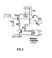
- FIG. 2 The detailed structure of the crosspoint circuits with control is shown in FIG. 2.
- m 1 - 3 and m2 4 selected.
- the connected outputs of m 1 crosspoints each work on a self-locking base stage BSmn.
- BSmn self-locking base stage
- four basic levels are required per column.
- the outputs of these basic stages work again on a common load resistance R L.
- the optimum of m 2 (number of blocks) depends on the boundary conditions.
- the base stages BSmn of each column are connected to one another on the output side and lead to a common load resistance RL per column.
- One decoupling level EK1, EK2, EK3, ... is provided for each line at the input.
- Each column also has a decoupling stage AK1, AK2, ... at the output - A1, A2 -.
- the special design of the decoupling stages EKm and AKn will be discussed in more detail in the description of FIG. 3.
- a single crosspoint circuit is shown in FIG.
- An emitter stage ESmn is supplied with the signal u E to be switched through at its base.
- a series circuit comprising a negative feedback resistor RG and the switching path of a transistor T is located in the emitter branch of ESmn.
- the transistors ESmn and T are npn transistors. Due to the series negative feedback of the emitter stage by means of the negative feedback resistor RG, the input impedance of the crosspoint circuits is so high that the signal delay time through the matrix depends only slightly on the number of crosspoints switched through per line.
- a switch S is connected in parallel to the base-emitter path of the transistor T, by means of which the switching paths are selected.
- switch S When switch S is open, transistor T is saturated and the coupling point is switched through.
- the switch S as part of a 1 L logic is activated by a control circuit (not shown).
- the holding members are also not shown.
- the switch in FIG. 2 if the switch in FIG. 2 is closed, T is blocked and the coupling point is therefore switched off. Since the current through R 1 is much less than I CES (z. B. I CES / 5 ... I CES / 10), so the power consumption is considerably lower than in the switched-on coupling point. But even when switched on, the power consumption is relatively small, since you can get by with a small supply voltage U 2 and (despite the high bit rate) with a small switching current I CES .
- the decoupling stage designated EKm in FIG. 1 follows the input E in the row direction. It consists of a differential amplifier - transistors T 1 and T 2 - and an emitter follower (collector stage T 6 ) connected downstream of the differential amplifier.
- the transistor T 3 with resistor R 3 connected in series is located in the common emitter line of T 1 and T 2 .
- a negative feedback resistor R may be inserted 1 (dotted line) and also a feedback resistor R1 in the emitter branch of T 2.
- the two reference voltages U R1 and U R2 for the transistors T 2 and T 3 are generated by an internal voltage divider in the manner customary in ECL circuits.
- the differential amplifier stage - T 1 , T 2 - converts the ECL level at input E to an internal, more favorable voltage level. In consideration of a small product of switching time and power loss, the stroke is reduced to approx. 500 mV.
- the output of the collector stage T 6 is connected to the actual cross point circuit KP.
- the collector stage T 6 is used for level shifting and for driving the row line with the attacking coupling point circuits KP.
- the coupling point circuit KP consists of the emitter stage T a , in the emitter current branch of which there is a negative feedback resistor R 7 and in series with the collector-emitter path of the transistor T 7 .
- the crosspoint circuit is activated by a control signal which opens the switch S (cf. description of FIG. 2).
- the emitter of T 7 is connected to the supply voltage U 2 , for example -2.5V.
- m crosspoints of a column, as in FIG. 1, are combined to form m 2 blocks with m 1 elements each.
- the comparatively large column capacity C 2 (FIG. 2) has to be reloaded solely by the coupling point switched on.
- the current i CES (amplitude I CES ) would approximately apply if the current jumped: where ⁇ u A is the voltage swing. It can be seen that, taking into account a small switching current I CES (ie small power loss), the smallest possible voltage swing must strive on the column in order to achieve a sufficiently large slope (ie large maximum bit rate).
- a smaller column stroke can be achieved by switching a base stage between the coupling point and the load resistor.
- the outputs of the m 1 emitter stages are therefore connected to a self-blocking base stage (transistor T 9 ) (FIG. 3).
- the outputs of the m 2 basic stages work on the load resistor R 12 .
- R 12 corresponds to the load resistance RL of FIG. 1.
- the basic stages enable steep pulse edges in spite of the high capacitive load on the internal gaps and increase - particularly for m 2 > 1 - the blocking damping.
- the voltage divider R 8 - R 9 lowers the bias voltage at the input of the blocked base stage so that the signal delay does not increase excessively during long pulse pauses and nevertheless reliably blocks the base stage.
- the voltage divider R 10 -R 11 allows the distance of the transistor T9 from the saturation limit to be increased if necessary.
- the output-side decoupling stage consists of an emitter follower stage for level shifting and reducing the load on the base stage - transistor T 10 -, a differential amplifier stage - transistors T 11 and T 12 -, in whose common emitter line a transistor T 13 for emitter current injection similar to the differential amplifier is inserted at the input , and a further emitter follower stage - transistor T 14 .
- the power switch consisting of T 11 , T 12 and T 13 , the impulses on the column are regenerated and amplified by a factor of 2 to the usual ECL strokes.
- the further emitter follower T 14 is dimensioned so that it can drive closed lines. If all crosspoints of a column are switched off, the associated output is at the L level.
- a compensation stage is arranged between the input-side differential amplifier - T 1 , T 2 - and the collector stage - T 6 . Through them, the current through the crosspoint circuit and thus the voltage swing on the internal Column (at the load resistor R 12 ) approximately independent of fluctuations in the supply voltage U 2 , the temperature and the output voltage of the transistor T 7 .
- the compensation stage consists of two transistors T 4 and T 59 whose collector-emitter paths are connected in series with one another via a series resistor R 4 .
- the first transistor T 4 is connected on the collector side to the output of the input differential amplifier transistors - T 19 T 2 - and on the emitter side to the series resistor R 4 .
- the second transistor T 5 is connected on the collector side to the series resistor R 4 and is connected to the supply voltage U 2 on the emitter side.
- the base connection of the first transistor T 4 is connected via a voltage divider R 5 - R 6 , which is between ground and supply voltage.
- a diode D is inserted into the branch of the voltage divider R 5 -R 6 adjacent to the ground connection.
- the influence of a change in the collector path resistance r c7 from T 7 on the collector current I CT8 can be largely compensated for by suitable dimensioning of the resistors and transistors of the compensation network .
- the transistor T 5 with the path resistance r c5 which is operated like transistor T 7 in saturation, is used for this purpose.
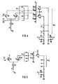
- the crosspoint circuit consists of a symmetrical current switch - transistors T 15 , T 16 -. This is similar to that in FIG. 3 built-up input-side decoupling stage (not shown), the signal passed via terminals K1 and K2 to the base connections of transistors T15 and T16.
- the common emitter branch of T15 and T16 there is a current source Q which can be switched via the switch S which is connected to the supply voltage U 2 and with which the coupling points to be switched through are selected.
- the collectors of the transistors T 15 and T 16 are each connected to a base stage T 17 and T18.
- the crosspoint circuit in FIG. 5 is constructed similarly to that in FIG. 4, but now as an asymmetrical current switch. Only the transistor T 15 is driven with the signal from the input-side decoupling stage. Its collector is connected to ground potential. The transistor T 16 is supplied with a reference voltage U ref on the base side . The subsequent basic stage - T 17 - which is only available once per block is sent to its collector. connected. m 2 of such basic stages - T 17 - work on a common load resistor RL with a Schottky diode SD connected in parallel.
Landscapes
- Engineering & Computer Science (AREA)
- Computer Networks & Wireless Communication (AREA)
- Electronic Switches (AREA)
- Use Of Switch Circuits For Exchanges And Methods Of Control Of Multiplex Exchanges (AREA)
Applications Claiming Priority (2)
| Application Number | Priority Date | Filing Date | Title |
|---|---|---|---|
| DE3400217 | 1984-01-05 | ||
| DE3400217 | 1984-01-05 |
Publications (3)
| Publication Number | Publication Date |
|---|---|
| EP0148395A2 true EP0148395A2 (fr) | 1985-07-17 |
| EP0148395A3 EP0148395A3 (en) | 1988-03-23 |
| EP0148395B1 EP0148395B1 (fr) | 1991-02-06 |
Family
ID=6224373
Family Applications (1)
| Application Number | Title | Priority Date | Filing Date |
|---|---|---|---|
| EP84114456A Expired - Lifetime EP0148395B1 (fr) | 1984-01-05 | 1984-11-29 | Champ de couplage à large bande sous forme de matrice |
Country Status (5)
| Country | Link |
|---|---|
| US (1) | US4630046A (fr) |
| EP (1) | EP0148395B1 (fr) |
| JP (1) | JPS60160294A (fr) |
| CA (1) | CA1228128A (fr) |
| DE (1) | DE3484101D1 (fr) |
Cited By (5)
| Publication number | Priority date | Publication date | Assignee | Title |
|---|---|---|---|---|
| WO1989001262A3 (fr) * | 1987-07-29 | 1989-02-23 | Fujitsu Ltd | Circuit electronique a haute vitesse presentant une configuration cascode |
| DE4010283A1 (de) * | 1990-03-30 | 1991-10-02 | Fraunhofer Ges Forschung | Koppelfeldmatrixschaltung |
| US5510745A (en) * | 1987-07-29 | 1996-04-23 | Fujitsu Limited | High-speed electronic circuit having a cascode configuration |
| DE19959426C1 (de) * | 1999-12-09 | 2001-01-18 | Siemens Ag | Koppelelement und Koppelanordnung |
| DE10337416B3 (de) * | 2003-08-14 | 2005-05-04 | Siemens Ag | Kreuzschienenverteiler |
Families Citing this family (6)
| Publication number | Priority date | Publication date | Assignee | Title |
|---|---|---|---|---|
| ATE41249T1 (de) * | 1984-09-05 | 1989-03-15 | Siemens Ag | Anordnung zur prioritaetsvergabe. |
| JPH02500238A (ja) * | 1987-07-29 | 1990-01-25 | 富士通株式会社 | カスコード構成の高速電子回路 |
| US4845722A (en) * | 1987-10-16 | 1989-07-04 | Digital Equipment Corporation | Computer interconnect coupler employing crossbar switching |
| DE3802579A1 (de) * | 1988-01-29 | 1989-08-10 | Ant Nachrichtentech | Dreistufiges blockierungsfreies koppelfeld |
| DE3938459A1 (de) * | 1989-11-20 | 1991-05-23 | Philips Patentverwaltung | Schaltungsanordnung zur kompensation von impulslaengenveraenderungen |
| JP2701513B2 (ja) * | 1990-03-29 | 1998-01-21 | 日本電気株式会社 | 回線切替制御方式 |
Family Cites Families (13)
| Publication number | Priority date | Publication date | Assignee | Title |
|---|---|---|---|---|
| US28224A (en) * | 1860-05-08 | Musical | ||
| US3550087A (en) * | 1968-03-26 | 1970-12-22 | Central Dynamics | Video switching circuit |
| USRE28224E (en) | 1968-10-28 | 1974-11-05 | Transistor matrix | |
| US3636384A (en) * | 1970-09-14 | 1972-01-18 | Ibm | Base-to-emitter compensation for current switch emitter-follower circuits |
| DE2451728B2 (de) * | 1974-10-31 | 1977-10-06 | Licentia Patent-Verwaltungs-Gmbh, 6000 Frankfurt | Elektronischer koppelpunkt zur gerichteten durchschaltung von breitbandsignalen |
| DE2917989A1 (de) * | 1979-05-04 | 1980-11-13 | Bosch Gmbh Robert | Elektronische koppelfeldeinrichtung |
| DE2932587C2 (de) | 1979-08-10 | 1983-12-01 | Siemens AG, 1000 Berlin und 8000 München | Breitbandkoppelanordnung mit einer Matrix von Koppelpunktschaltkreisen in ECL-Technik |
| DE2944794C2 (de) * | 1979-11-06 | 1981-11-12 | Siemens AG, 1000 Berlin und 8000 München | Breitband-Koppelanordnung |
| DE3101932A1 (de) * | 1981-01-22 | 1982-09-02 | Licentia Patent-Verwaltungs-Gmbh, 6000 Frankfurt | "koppelfeld in matrixform fuer signalfrequenzen im megahertzbereich" |
| US4446552A (en) * | 1981-12-21 | 1984-05-01 | Gte Laboratories Incorporated | Wideband switch crosspoint and switching matrix |
| FR2519211A1 (fr) | 1981-12-30 | 1983-07-01 | Radiotechnique Compelec | Etage de sortie pour circuit integre a reseau de portes de la technique ecl regule vis-a-vis des variations liees aux temperatures de fonctionnement |
| DE3215176A1 (de) | 1982-04-23 | 1983-10-27 | Licentia Patent-Verwaltungs-Gmbh, 6000 Frankfurt | Monolithisch integrierter koppelbaustein |
| US4516238A (en) * | 1983-03-28 | 1985-05-07 | At&T Bell Laboratories | Self-routing switching network |
-
1984
- 1984-11-29 EP EP84114456A patent/EP0148395B1/fr not_active Expired - Lifetime
- 1984-11-29 DE DE8484114456T patent/DE3484101D1/de not_active Revoked
- 1984-12-27 JP JP59274240A patent/JPS60160294A/ja active Pending
- 1984-12-31 US US06/688,161 patent/US4630046A/en not_active Expired - Fee Related
-
1985
- 1985-01-04 CA CA000471475A patent/CA1228128A/fr not_active Expired
Cited By (7)
| Publication number | Priority date | Publication date | Assignee | Title |
|---|---|---|---|---|
| WO1989001262A3 (fr) * | 1987-07-29 | 1989-02-23 | Fujitsu Ltd | Circuit electronique a haute vitesse presentant une configuration cascode |
| US5510745A (en) * | 1987-07-29 | 1996-04-23 | Fujitsu Limited | High-speed electronic circuit having a cascode configuration |
| DE4010283A1 (de) * | 1990-03-30 | 1991-10-02 | Fraunhofer Ges Forschung | Koppelfeldmatrixschaltung |
| DE19959426C1 (de) * | 1999-12-09 | 2001-01-18 | Siemens Ag | Koppelelement und Koppelanordnung |
| US6437633B2 (en) | 1999-12-09 | 2002-08-20 | Siemens Aktiengesellschaft | Switching element, stage and system |
| DE10337416B3 (de) * | 2003-08-14 | 2005-05-04 | Siemens Ag | Kreuzschienenverteiler |
| US7064628B2 (en) | 2003-08-14 | 2006-06-20 | Siemens Aktiengesellschaft | Crossbar switch |
Also Published As
| Publication number | Publication date |
|---|---|
| US4630046A (en) | 1986-12-16 |
| JPS60160294A (ja) | 1985-08-21 |
| DE3484101D1 (de) | 1991-03-14 |
| EP0148395A3 (en) | 1988-03-23 |
| EP0148395B1 (fr) | 1991-02-06 |
| CA1228128A (fr) | 1987-10-13 |
Similar Documents
| Publication | Publication Date | Title |
|---|---|---|
| EP0096944B1 (fr) | Circuit avec plusieurs chemins de signaux formés par des composants actifs | |
| DE3743969C2 (fr) | ||
| DE3904901C2 (fr) | ||
| DE69311824T2 (de) | Schaltung mit veränderlicher Verzögerung | |
| DE69019665T2 (de) | CMOS-Treiberschaltung. | |
| DE2625007B2 (de) | Adressenpufferschaltung für Halbleiterspeicher | |
| EP0148395B1 (fr) | Champ de couplage à large bande sous forme de matrice | |
| DE2036306A1 (de) | Mehrfachverstärker, insbesondere in integrierter Schaltung, mit Stufenentkopplung | |
| DE4010145C1 (fr) | ||
| DE3525522C2 (fr) | ||
| EP0345623A2 (fr) | Dispositif de commutation pour signaux à large bande | |
| DE3407800C2 (fr) | ||
| EP0057239B1 (fr) | Circuit d'attaque du type push-pull monolithiquement intégré | |
| DE3602551C2 (de) | Operationsverstärker | |
| DE68928576T2 (de) | Digitalverstärker und diesen enthaltende integrierte Schaltung | |
| DE3712998C2 (fr) | ||
| DE3801530C2 (fr) | ||
| DE4231178C2 (de) | Speicherelement | |
| EP0015364A1 (fr) | Multivibrateur utilisant des transistors à effet de champ | |
| DE3151080C2 (de) | Koppelfeldeinrichtung | |
| DE3209862C2 (de) | Leistungsstufe für zwei erdsymmetrische binäre Ausgangssignale | |
| EP1041709B1 (fr) | Circuit oscillateur | |
| DE2246756B2 (de) | Elektronischer Datenspeicher | |
| DE69010126T2 (de) | Integrierte, programmierbare Logikanordnung. | |
| DE4222468C1 (en) | CMOS inverter stage using additional FET - placed between FETs as diode with gate terminal connected to input terminal |
Legal Events
| Date | Code | Title | Description |
|---|---|---|---|
| PUAI | Public reference made under article 153(3) epc to a published international application that has entered the european phase |
Free format text: ORIGINAL CODE: 0009012 |
|
| AK | Designated contracting states |
Designated state(s): DE FR GB NL SE |
|
| PUAL | Search report despatched |
Free format text: ORIGINAL CODE: 0009013 |
|
| AK | Designated contracting states |
Kind code of ref document: A3 Designated state(s): DE FR GB NL SE |
|
| 17P | Request for examination filed |
Effective date: 19880212 |
|
| 17Q | First examination report despatched |
Effective date: 19891108 |
|
| GRAA | (expected) grant |
Free format text: ORIGINAL CODE: 0009210 |
|
| AK | Designated contracting states |
Kind code of ref document: B1 Designated state(s): DE FR GB NL SE |
|
| GBT | Gb: translation of ep patent filed (gb section 77(6)(a)/1977) | ||
| REF | Corresponds to: |
Ref document number: 3484101 Country of ref document: DE Date of ref document: 19910314 |
|
| ET | Fr: translation filed | ||
| PLBI | Opposition filed |
Free format text: ORIGINAL CODE: 0009260 |
|
| PG25 | Lapsed in a contracting state [announced via postgrant information from national office to epo] |
Ref country code: GB Effective date: 19911129 |
|
| PG25 | Lapsed in a contracting state [announced via postgrant information from national office to epo] |
Ref country code: SE Effective date: 19911130 |
|
| 26 | Opposition filed |
Opponent name: SIEMENS AKTIENGESELLSCHAFT, BERLIN UND MUENCHEN Effective date: 19911105 |
|
| NLR1 | Nl: opposition has been filed with the epo |
Opponent name: SIEMENS AG. |
|
| PG25 | Lapsed in a contracting state [announced via postgrant information from national office to epo] |
Ref country code: NL Effective date: 19920601 |
|
| NLV4 | Nl: lapsed or anulled due to non-payment of the annual fee | ||
| GBPC | Gb: european patent ceased through non-payment of renewal fee | ||
| PG25 | Lapsed in a contracting state [announced via postgrant information from national office to epo] |
Ref country code: FR Effective date: 19920731 |
|
| REG | Reference to a national code |
Ref country code: FR Ref legal event code: ST |
|
| PGFP | Annual fee paid to national office [announced via postgrant information from national office to epo] |
Ref country code: DE Payment date: 19940118 Year of fee payment: 10 |
|
| EUG | Se: european patent has lapsed |
Ref document number: 84114456.1 Effective date: 19920604 |
|
| RDAG | Patent revoked |
Free format text: ORIGINAL CODE: 0009271 |
|
| STAA | Information on the status of an ep patent application or granted ep patent |
Free format text: STATUS: PATENT REVOKED |
|
| 27W | Patent revoked |
Effective date: 19941226 |