EP0345623A2 - Dispositif de commutation pour signaux à large bande - Google Patents
Dispositif de commutation pour signaux à large bande Download PDFInfo
- Publication number
- EP0345623A2 EP0345623A2 EP89109840A EP89109840A EP0345623A2 EP 0345623 A2 EP0345623 A2 EP 0345623A2 EP 89109840 A EP89109840 A EP 89109840A EP 89109840 A EP89109840 A EP 89109840A EP 0345623 A2 EP0345623 A2 EP 0345623A2
- Authority
- EP
- European Patent Office
- Prior art keywords
- transistor
- matrix
- tpi
- signal
- transistors
- Prior art date
- Legal status (The legal status is an assumption and is not a legal conclusion. Google has not performed a legal analysis and makes no representation as to the accuracy of the status listed.)
- Granted
Links
Images


Classifications
-
- H—ELECTRICITY
- H04—ELECTRIC COMMUNICATION TECHNIQUE
- H04Q—SELECTING
- H04Q3/00—Selecting arrangements
- H04Q3/42—Circuit arrangements for indirect selecting controlled by common circuits, e.g. register controller, marker
- H04Q3/52—Circuit arrangements for indirect selecting controlled by common circuits, e.g. register controller, marker using static devices in switching stages, e.g. electronic switching arrangements
- H04Q3/521—Circuit arrangements for indirect selecting controlled by common circuits, e.g. register controller, marker using static devices in switching stages, e.g. electronic switching arrangements using semiconductors in the switching stages
Definitions
- the ECL technology can be characterized by properties such as high working speed, (medium) high degree of integration and (medium) high power loss
- the FET technology is characterized by a very high degree of integration and very low, in contrast to only medium working speeds Power losses.
- this known broadband signal coupling device has the further advantage that, on the one hand, when the crosspoint is blocked, no interfering signals reach the matrix output via the crosspoint without additional attenuation measures that on the other hand - in the case of a conductive coupling point - during the actual bit switching, the transhipment of the matrix output line, if any, always proceeds from the one operating potential corresponding to the one signal state in only one reversal direction and thus already with a (the exceeding of an operating potential value adjacent to this, the tipping point of the Differential amplifier corresponding threshold corresponding) small transfer - and thus correspondingly quickly - a clear transition of the switched-through digital signal occurring at the output of the coupling device from one signal state to the other d is connected.
- the object of the invention is now to enable a further increase in the operating speed in such a broadband signal coupling device.
- the invention thus relates to a broadband signal coupling device with a crosspoint matrix in FET technology, each of which has matrix input lines formed with two signal conductors, the two signal conductors of which are each connected to the two differential (complementary) outputs of two such differential (complementary) outputs.
- Input digital signal circuit having outputs are connected and, on the other hand, can be connected via the coupling points formed with coupling element pairs to matrix output lines, each also formed with two signal conductors, each of which leads with its two signal conductors to the two signal inputs of an output amplifier circuit formed with a differential amplifier with a tilting behavior, wherein the coupling element pairs are each formed with two switch transistors to which a switch-through or blocking signal is applied to the control electrode and a main electrode to one or the other signal conductor of the associated matrix output line, wherein the coupling element pairs each have two ballast transistors forming a series circuit with a switch transistor, which are each connected to the control electrode on one or the other signal conductor of the associated matrix input line and whose respective main electrode facing away from the series circuit is connected via a scanning transistor to the one connection of the operating voltage source, with the other connection of each signal conductor of the respective matrix output line in each case via a precharge transistor is connected and wherein precharge transistors and sense transistors are applied in opposite directions to each other
- the invention has the further advantage of a very early potential symmetry of the matrix output lines, so that the initial conditions for safe amplification by a subsequent differential amplifier are also given in good time.
- a further increase in the operating speed of the wideband signal coupling device is obtained if, in a further embodiment of the invention, in addition to a matrix input line-individual scanning transistor, a matrix input line-specific precharge transistor or, alternatively, in addition to a matrix output line-individual scanning transistor, a matrix output line-individual Precharge transistor is provided.
- a broadband signal coupling device (known from EP-AO 264 046) is schematically sketched, at whose coupling lines sl ... sj ... sn a coupling point matrix leading inputs el ... ej ... en input digital signal circuits El ... Ej ... En are provided and their outputs reached by row lines zl ... zi ... zm the cross point matrix al ... ai ... am are provided with output amplifier circuits Al ... Ai ... Am.
- the crosspoint matrix has crosspoints KPll ... KPij ...
- the matrix input lines are each with two signal conductors sl ', sl ⁇ ; ...; sj ', sj ⁇ ; ...; sn', sn ⁇ formed, each of complementary (differential) outputs of the respective associated, in FIG 1 as an amplifier with a non-inverting and an inverting output, i.e. Input digital signal circuit El, ..., Ej, ..., En shown as a so-called differential line driver are connected.
- sj ′, sj ⁇ ; ... ...; sn ′, sn ⁇ are, on the other hand, via coupling points KPll, ..., KPij, ..., KPnm with matrix output lines (Kij at the coupling point KPij in FIG. 1) Row lines) connected, each with two signal conductors zl ', zl ⁇ ; ...; zi', zi ⁇ ; ...; zm ', zm ⁇ are formed and each lead to the two signal inputs of an output amplifier circuit Al, .., Ai, ..., Am formed with a differential amplifier with a tilting behavior.
- Such a differential amplifier with tilting behavior can be implemented with a so-called gated flip-flop, as described in Principle (from
- ) should expediently be designed as a p-channel transistor; a further implementation possibility is known from EP-AO 264 046, FIG. 5.
- FIG. 2, FIG. 3 and FIG. 4 How the coupling element pairs ... Kij ... can be implemented in terms of circuit technology is illustrated in FIG. 2, FIG. 3 and FIG. 4: The two each acted upon with a switch-through or blocking signal on the control electrode and with a main electrode on one or the other signal conductors zi ', zi ⁇ of the associated matrix output line connected switch transistors Tnk', Tnk ⁇ formed coupling element pairs ... Kij ...
- Tna namely Tnaij in FIG. 2 or Tnaj in FIG. 3 or Tnai in FIG. 4
- the two signal conductors (zi ', zi ⁇ ) of the respective matrix output line (row line) ... zi ... are each connected via a precharging transistor Tpi' or Tpi ⁇ ; at their respective matrix output line (zi ', zi ⁇ ) facing main electrodes, the two precharging transistors Tpi', Tpi ⁇ are connected to one another via a cross transistor Tpi ′′′, the control electrode of which is connected to the control electrodes of the precharging transistors Tpi ', Tpi ⁇ .
- a coupling transistor pair Tnaij can be provided in each case; alternatively, however, as shown in FIG. 3, a common and thus matrix input line-individual scanning transistor (Tnaj in FIG. 3) can be provided for all of the coupling element pairs lying on one and the same matrix input line (column line) ..sj .., or it As can be seen from FIG. 4, a coupling transistor common to all of the coupling element pairs lying on one and the same matrix output line (row line) ... zi ... and thus individual matrix output line (Tnai in FIG. 4) can be provided. In this case, as can be seen from FIG.
- a precharge transistor Tpaj that is individual to the matrix input line can be provided in addition to a sampling transistor Tnaj that is individual to the matrix input line, and, as can be seen from FIG.
- Transistor Tnai a matrix output line individual precharge transistor Tpai can be provided.
- the switch transistors Tnk, the ballast transistors Tne and scan transistors Tna can be n-channel transistors and the precharge transistors Tpi - with a cross-point matrix held in CMOS technology p-channel transistors.
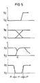
- Precharge transistors Tpi and sampling transistors Tna are applied in opposite directions to each other at their control electrode with a clock switching period indicated in FIG. 5, below, in a pre-phase pv and a main phase ph clock T, as shown in FIG Line T is indicated.
- the transverse transistor Tpi ′′′ lying between the two signal conductors zi ', zi ⁇ becomes conductive with the result of a short circuit of the two signal conductors zi', zi ⁇ , due to which it is very fast at the beginning of the pre-phase ( Time t1 in FIG.
- the sampling transistors Tna (Tnaj in FIG. 2, Tnaj in FIG. 3, Tnai in FIG. 4) formed by n-channel transistors are used in the example the same "low" clock signal T driven in the opposite sense, ie locked, so that the charging of the two signal conductors (zi ', zi ⁇ ) of the matrix output lines (row lines) ... zi ...
- the pseudo ground line PM is charged during the pre-phase pv via this precharge transistor (Tpaj in FIG. 3; Tpai in FIG. 4) , with which the respective coupling element pair ... Kij ... is relieved.
- this precharge transistor Tpaj in FIG. 3; Tpai in FIG. 4
- Switch-through signals are conductive and the crosspoint is in the switch-through state, so depending on the bit to be switched, the two signal conductors sj ′, sj ⁇ of the relevant matrix input line (column line) ... sj ... prevailing signal states, the signal conductors zi ′, zi ⁇ of the matrix input line (column line) ... sj ...
- the “high” signal state prevails and is accordingly the ballast transistor Tne ′ or Tne ⁇ (in FIG. 2 to FIG. 4) of the coupling element pair Kij under consideration just like the switch transistor Tnk 'or Tnk ⁇ and the associated sampling transistor Tna conductive, the assigned signal conductor zi' or zi ⁇ of the matrix output line (row line) zi is discharged via this coupling element of the coupling element pair Kij and onto the U SS -Potential pulled.
- the respective input signal is thus switched through in an inverted manner via a coupling point unlocked from its control input s.
- the precharge transistors (Tpi ', Tpi ⁇ ) are formed by p-channel transistors, these p-channel precharge transistors (Tpi) and those by n- Channel transistors formed sampling transistors (Tna), due to the different channel type, can be controlled in opposite directions to one another by one and the same signal (T).
- the precharge transistors with n-channel transistors, so that, even if the switch transistors (Tnk), the ballast transisto ren (Tne) and the sampling transistors (Tna) are n-channel transistors, only transistors of the same channel type are used; So that precharging transistors and sampling transistors are in turn applied in opposite directions to each other at their control electrode with the switching matrix drive clock, the sampling transistors (Tna) is again, as in the exemplary embodiments described with reference to FIGS. 2 to 4, that To feed the switching matrix drive clock signal (T) directly to the (n-channel) precharging transistors, however, the inverted switching matrix drive clock signal.
Landscapes
- Engineering & Computer Science (AREA)
- Computer Networks & Wireless Communication (AREA)
- Electronic Switches (AREA)
- Use Of Switch Circuits For Exchanges And Methods Of Control Of Multiplex Exchanges (AREA)
- Stereo-Broadcasting Methods (AREA)
- Circuits Of Receivers In General (AREA)
- Input Circuits Of Receivers And Coupling Of Receivers And Audio Equipment (AREA)
Priority Applications (1)
| Application Number | Priority Date | Filing Date | Title |
|---|---|---|---|
| AT89109840T ATE100264T1 (de) | 1988-06-08 | 1989-05-31 | Breitbandsignal-koppeleinrichtung. |
Applications Claiming Priority (2)
| Application Number | Priority Date | Filing Date | Title |
|---|---|---|---|
| DE3819491 | 1988-06-08 | ||
| DE3819491 | 1988-06-08 |
Publications (3)
| Publication Number | Publication Date |
|---|---|
| EP0345623A2 true EP0345623A2 (fr) | 1989-12-13 |
| EP0345623A3 EP0345623A3 (en) | 1990-05-23 |
| EP0345623B1 EP0345623B1 (fr) | 1994-01-12 |
Family
ID=6356119
Family Applications (1)
| Application Number | Title | Priority Date | Filing Date |
|---|---|---|---|
| EP89109840A Expired - Lifetime EP0345623B1 (fr) | 1988-06-08 | 1989-05-31 | Dispositif de commutation pour signaux à large bande |
Country Status (9)
| Country | Link |
|---|---|
| US (1) | US4949086A (fr) |
| EP (1) | EP0345623B1 (fr) |
| JP (1) | JP2773043B2 (fr) |
| AT (1) | ATE100264T1 (fr) |
| CA (1) | CA1320259C (fr) |
| DE (1) | DE58906667D1 (fr) |
| HU (1) | HU205691B (fr) |
| LU (1) | LU87431A1 (fr) |
| RU (1) | RU2103831C1 (fr) |
Cited By (5)
| Publication number | Priority date | Publication date | Assignee | Title |
|---|---|---|---|---|
| EP0451312A1 (fr) * | 1990-04-12 | 1991-10-16 | Siemens Aktiengesellschaft | Dispositif de commutation pour signaux à large bande |
| EP0456857A1 (fr) * | 1990-05-16 | 1991-11-21 | Siemens Aktiengesellschaft | Circuit numérique avec compensation de potentiel entre deux conducteurs de signaux |
| DE4030596C1 (en) * | 1990-09-27 | 1991-12-12 | Siemens Ag, 8000 Muenchen, De | Wideband signal coupling circuitry with large number of outputs - connectable to leads loadable w.r.t. earth by own capacitance and/or loading capacitors |
| EP0388856A3 (fr) * | 1989-03-22 | 1992-03-25 | Siemens Aktiengesellschaft | Dispositif de couplage pour signaux à large bande |
| EP0573637A4 (fr) * | 1991-12-26 | 1994-03-16 | Altera Corporation |
Families Citing this family (6)
| Publication number | Priority date | Publication date | Assignee | Title |
|---|---|---|---|---|
| FR2650452B1 (fr) * | 1989-07-27 | 1991-11-15 | Sgs Thomson Microelectronics | Point de croisement pour matrice de commutation |
| ATE105662T1 (de) * | 1989-09-11 | 1994-05-15 | Siemens Ag | Breitbandsignal-koppeleinrichtung. |
| JPH05199255A (ja) * | 1992-01-18 | 1993-08-06 | Mitsubishi Electric Corp | 電子クロスポイントスイッチ装置 |
| US5506528A (en) * | 1994-10-31 | 1996-04-09 | International Business Machines Corporation | High speed off-chip CMOS receiver |
| US6984870B2 (en) * | 2002-10-18 | 2006-01-10 | M/A-Com, Inc. | High speed cross-point switch using SiGe HBT technology |
| US6998935B2 (en) * | 2003-02-19 | 2006-02-14 | M/A-Com, Inc. | Switch matrix |
Family Cites Families (8)
| Publication number | Priority date | Publication date | Assignee | Title |
|---|---|---|---|---|
| JPS5040246A (fr) * | 1973-08-03 | 1975-04-12 | ||
| US4004284A (en) * | 1975-03-05 | 1977-01-18 | Teletype Corporation | Binary voltage-differential sensing circuits, and sense/refresh amplifier circuits for random-access memories |
| DE2932587C2 (de) * | 1979-08-10 | 1983-12-01 | Siemens AG, 1000 Berlin und 8000 München | Breitbandkoppelanordnung mit einer Matrix von Koppelpunktschaltkreisen in ECL-Technik |
| US4577190A (en) * | 1983-04-11 | 1986-03-18 | At&T Bell Laboratories | Programmed logic array with auxiliary pull-up means to increase precharging speed |
| US4750155A (en) * | 1985-09-19 | 1988-06-07 | Xilinx, Incorporated | 5-Transistor memory cell which can be reliably read and written |
| LU86456A1 (de) * | 1985-11-04 | 1986-11-13 | Siemens Ag | Breitbandsignal-raumkoppeleinrichtung |
| LU86790A1 (de) * | 1986-09-17 | 1987-07-24 | Siemens Ag | Breitbandsignal-koppeleinrichtung |
| LU86915A1 (de) * | 1986-10-07 | 1987-11-11 | Siemens Ag | Breitbandsignal-koppeleinrichtung |
-
1989
- 1989-01-18 LU LU87431A patent/LU87431A1/de unknown
- 1989-05-17 US US07/353,044 patent/US4949086A/en not_active Expired - Lifetime
- 1989-05-29 RU SU4614163A patent/RU2103831C1/ru active
- 1989-05-31 AT AT89109840T patent/ATE100264T1/de not_active IP Right Cessation
- 1989-05-31 DE DE89109840T patent/DE58906667D1/de not_active Expired - Fee Related
- 1989-05-31 EP EP89109840A patent/EP0345623B1/fr not_active Expired - Lifetime
- 1989-06-05 JP JP1142870A patent/JP2773043B2/ja not_active Expired - Fee Related
- 1989-06-06 CA CA000601881A patent/CA1320259C/fr not_active Expired - Fee Related
- 1989-06-07 HU HU892912A patent/HU205691B/hu not_active IP Right Cessation
Cited By (7)
| Publication number | Priority date | Publication date | Assignee | Title |
|---|---|---|---|---|
| EP0388856A3 (fr) * | 1989-03-22 | 1992-03-25 | Siemens Aktiengesellschaft | Dispositif de couplage pour signaux à large bande |
| EP0451312A1 (fr) * | 1990-04-12 | 1991-10-16 | Siemens Aktiengesellschaft | Dispositif de commutation pour signaux à large bande |
| US5073775A (en) * | 1990-04-12 | 1991-12-17 | Siemens Aktiengesellschaft | Broadband signal switching equipment |
| EP0456857A1 (fr) * | 1990-05-16 | 1991-11-21 | Siemens Aktiengesellschaft | Circuit numérique avec compensation de potentiel entre deux conducteurs de signaux |
| DE4030596C1 (en) * | 1990-09-27 | 1991-12-12 | Siemens Ag, 8000 Muenchen, De | Wideband signal coupling circuitry with large number of outputs - connectable to leads loadable w.r.t. earth by own capacitance and/or loading capacitors |
| EP0573637A4 (fr) * | 1991-12-26 | 1994-03-16 | Altera Corporation | |
| US5517186A (en) * | 1991-12-26 | 1996-05-14 | Altera Corporation | EPROM-based crossbar switch with zero standby power |
Also Published As
| Publication number | Publication date |
|---|---|
| RU2103831C1 (ru) | 1998-01-27 |
| JPH0244892A (ja) | 1990-02-14 |
| EP0345623A3 (en) | 1990-05-23 |
| HU205691B (en) | 1992-05-28 |
| JP2773043B2 (ja) | 1998-07-09 |
| LU87431A1 (de) | 1989-06-14 |
| ATE100264T1 (de) | 1994-01-15 |
| EP0345623B1 (fr) | 1994-01-12 |
| DE58906667D1 (de) | 1994-02-24 |
| CA1320259C (fr) | 1993-07-13 |
| US4949086A (en) | 1990-08-14 |
Similar Documents
| Publication | Publication Date | Title |
|---|---|---|
| DE2544974C3 (de) | Schaltkreis zur Realisierung logischer Funktionen | |
| DE2222521C3 (de) | N-stufiger Ringzähler | |
| DE2721851A1 (de) | Verriegelnder leseverstaerker fuer halbleiterspeicheranordnungen | |
| DE2840578A1 (de) | Abtast-verstaerker | |
| EP0262479B1 (fr) | Dispositif de commutation pour signaux à large bande | |
| DE1462952A1 (de) | Schaltungsanordnung zur Realisierung logischer Funktionen | |
| DE2608119A1 (de) | Schaltkreis zum abtasten und auffrischen eines halbleiterspeichers | |
| DE2726094A1 (de) | Programmierbare logik in matrixanordnung | |
| EP0345623B1 (fr) | Dispositif de commutation pour signaux à large bande | |
| EP0264046B1 (fr) | Dispositif de commutation pour signaux à large bande | |
| DE2802595C2 (de) | Schaltungsanordnung mit Feldeffekttransistoren zur Spannungspegelumsetzung | |
| DE4010145C1 (fr) | ||
| EP0451312B1 (fr) | Dispositif de commutation pour signaux à large bande | |
| EP0148395A2 (fr) | Champ de couplage à large bande sous forme de matrice | |
| EP0238834A1 (fr) | Dispositif de couplage spatial pour signaux à large bande | |
| EP0249836B1 (fr) | Dispositif de commutation pour signaux à large bande | |
| EP0354252B1 (fr) | Dispositif de couplage pour signaux à large bande | |
| EP0388856B1 (fr) | Dispositif de couplage pour signaux à large bande | |
| EP0417336B1 (fr) | Dispositif de commutation pour signaux à large bande | |
| EP0249837A1 (fr) | Dispositif de commutation pour signaux à large bande | |
| EP0311956B1 (fr) | Dispositif de couplage pour signaux large bande | |
| EP0408797B1 (fr) | Dispositif de couplage pour signaux large bande | |
| DE69010126T2 (de) | Integrierte, programmierbare Logikanordnung. | |
| DE1462952C (de) | Schaltungsanordnung zur Realisierung logischer Funktionen | |
| DE2348453C3 (de) | Koppelmatrix mit für sich bistabilen Koppelpunkten |
Legal Events
| Date | Code | Title | Description |
|---|---|---|---|
| PUAI | Public reference made under article 153(3) epc to a published international application that has entered the european phase |
Free format text: ORIGINAL CODE: 0009012 |
|
| AK | Designated contracting states |
Kind code of ref document: A2 Designated state(s): AT BE CH DE FR GB IT LI NL SE |
|
| PUAL | Search report despatched |
Free format text: ORIGINAL CODE: 0009013 |
|
| AK | Designated contracting states |
Kind code of ref document: A3 Designated state(s): AT BE CH DE FR GB IT LI NL SE |
|
| 17P | Request for examination filed |
Effective date: 19901108 |
|
| 17Q | First examination report despatched |
Effective date: 19930312 |
|
| GRAA | (expected) grant |
Free format text: ORIGINAL CODE: 0009210 |
|
| AK | Designated contracting states |
Kind code of ref document: B1 Designated state(s): AT BE CH DE FR GB IT LI NL SE |
|
| REF | Corresponds to: |
Ref document number: 100264 Country of ref document: AT Date of ref document: 19940115 Kind code of ref document: T |
|
| REF | Corresponds to: |
Ref document number: 58906667 Country of ref document: DE Date of ref document: 19940224 |
|
| ITF | It: translation for a ep patent filed | ||
| GBT | Gb: translation of ep patent filed (gb section 77(6)(a)/1977) |
Effective date: 19940321 |
|
| ET | Fr: translation filed | ||
| PLBE | No opposition filed within time limit |
Free format text: ORIGINAL CODE: 0009261 |
|
| STAA | Information on the status of an ep patent application or granted ep patent |
Free format text: STATUS: NO OPPOSITION FILED WITHIN TIME LIMIT |
|
| 26N | No opposition filed | ||
| EAL | Se: european patent in force in sweden |
Ref document number: 89109840.2 |
|
| PGFP | Annual fee paid to national office [announced via postgrant information from national office to epo] |
Ref country code: AT Payment date: 19970512 Year of fee payment: 9 |
|
| PGFP | Annual fee paid to national office [announced via postgrant information from national office to epo] |
Ref country code: NL Payment date: 19970523 Year of fee payment: 9 |
|
| PGFP | Annual fee paid to national office [announced via postgrant information from national office to epo] |
Ref country code: BE Payment date: 19970527 Year of fee payment: 9 |
|
| PGFP | Annual fee paid to national office [announced via postgrant information from national office to epo] |
Ref country code: CH Payment date: 19970819 Year of fee payment: 9 |
|
| PG25 | Lapsed in a contracting state [announced via postgrant information from national office to epo] |
Ref country code: LI Free format text: LAPSE BECAUSE OF NON-PAYMENT OF DUE FEES Effective date: 19980531 Ref country code: CH Free format text: LAPSE BECAUSE OF NON-PAYMENT OF DUE FEES Effective date: 19980531 Ref country code: BE Free format text: LAPSE BECAUSE OF NON-PAYMENT OF DUE FEES Effective date: 19980531 Ref country code: AT Free format text: LAPSE BECAUSE OF NON-PAYMENT OF DUE FEES Effective date: 19980531 |
|
| BERE | Be: lapsed |
Owner name: SIEMENS A.G. Effective date: 19980531 |
|
| PG25 | Lapsed in a contracting state [announced via postgrant information from national office to epo] |
Ref country code: NL Free format text: LAPSE BECAUSE OF NON-PAYMENT OF DUE FEES Effective date: 19981201 |
|
| REG | Reference to a national code |
Ref country code: CH Ref legal event code: PL |
|
| NLV4 | Nl: lapsed or anulled due to non-payment of the annual fee |
Effective date: 19981201 |
|
| PGFP | Annual fee paid to national office [announced via postgrant information from national office to epo] |
Ref country code: SE Payment date: 20010517 Year of fee payment: 13 |
|
| REG | Reference to a national code |
Ref country code: GB Ref legal event code: IF02 |
|
| PG25 | Lapsed in a contracting state [announced via postgrant information from national office to epo] |
Ref country code: SE Free format text: LAPSE BECAUSE OF NON-PAYMENT OF DUE FEES Effective date: 20020601 |
|
| EUG | Se: european patent has lapsed | ||
| PGFP | Annual fee paid to national office [announced via postgrant information from national office to epo] |
Ref country code: FR Payment date: 20030512 Year of fee payment: 15 |
|
| PGFP | Annual fee paid to national office [announced via postgrant information from national office to epo] |
Ref country code: GB Payment date: 20040427 Year of fee payment: 16 |
|
| PG25 | Lapsed in a contracting state [announced via postgrant information from national office to epo] |
Ref country code: FR Free format text: LAPSE BECAUSE OF NON-PAYMENT OF DUE FEES Effective date: 20050131 |
|
| REG | Reference to a national code |
Ref country code: FR Ref legal event code: ST |
|
| PG25 | Lapsed in a contracting state [announced via postgrant information from national office to epo] |
Ref country code: IT Free format text: LAPSE BECAUSE OF NON-PAYMENT OF DUE FEES;WARNING: LAPSES OF ITALIAN PATENTS WITH EFFECTIVE DATE BEFORE 2007 MAY HAVE OCCURRED AT ANY TIME BEFORE 2007. THE CORRECT EFFECTIVE DATE MAY BE DIFFERENT FROM THE ONE RECORDED. Effective date: 20050531 Ref country code: GB Free format text: LAPSE BECAUSE OF NON-PAYMENT OF DUE FEES Effective date: 20050531 |
|
| GBPC | Gb: european patent ceased through non-payment of renewal fee |
Effective date: 20050531 |
|
| PGFP | Annual fee paid to national office [announced via postgrant information from national office to epo] |
Ref country code: DE Payment date: 20060717 Year of fee payment: 18 |
|
| PG25 | Lapsed in a contracting state [announced via postgrant information from national office to epo] |
Ref country code: DE Free format text: LAPSE BECAUSE OF NON-PAYMENT OF DUE FEES Effective date: 20071201 |