EP0148504B2 - Procédé et appareil de pulvérisation - Google Patents
Procédé et appareil de pulvérisation Download PDFInfo
- Publication number
- EP0148504B2 EP0148504B2 EP84116391A EP84116391A EP0148504B2 EP 0148504 B2 EP0148504 B2 EP 0148504B2 EP 84116391 A EP84116391 A EP 84116391A EP 84116391 A EP84116391 A EP 84116391A EP 0148504 B2 EP0148504 B2 EP 0148504B2
- Authority
- EP
- European Patent Office
- Prior art keywords
- target
- magnetic field
- plasma
- substrate
- sputtering
- Prior art date
- Legal status (The legal status is an assumption and is not a legal conclusion. Google has not performed a legal analysis and makes no representation as to the accuracy of the status listed.)
- Expired - Lifetime
Links
- 238000004544 sputter deposition Methods 0.000 title claims description 59
- 238000000034 method Methods 0.000 title claims description 20
- 239000000758 substrate Substances 0.000 claims description 49
- 239000000463 material Substances 0.000 claims description 19
- 238000000151 deposition Methods 0.000 claims description 15
- 230000008021 deposition Effects 0.000 claims description 13
- 230000005684 electric field Effects 0.000 claims description 13
- 150000002500 ions Chemical class 0.000 claims description 12
- 239000010409 thin film Substances 0.000 claims description 8
- 239000013077 target material Substances 0.000 claims description 4
- 230000004907 flux Effects 0.000 description 13
- 239000002245 particle Substances 0.000 description 12
- 239000007789 gas Substances 0.000 description 10
- 150000001768 cations Chemical class 0.000 description 8
- 238000009826 distribution Methods 0.000 description 8
- 239000012212 insulator Substances 0.000 description 7
- 238000001755 magnetron sputter deposition Methods 0.000 description 7
- 230000000694 effects Effects 0.000 description 6
- 230000003628 erosive effect Effects 0.000 description 6
- 239000010408 film Substances 0.000 description 5
- VYPSYNLAJGMNEJ-UHFFFAOYSA-N silicon dioxide Inorganic materials O=[Si]=O VYPSYNLAJGMNEJ-UHFFFAOYSA-N 0.000 description 5
- 230000002093 peripheral effect Effects 0.000 description 4
- 230000008569 process Effects 0.000 description 4
- 229910052786 argon Inorganic materials 0.000 description 3
- 239000000470 constituent Substances 0.000 description 3
- 239000011261 inert gas Substances 0.000 description 3
- 230000007246 mechanism Effects 0.000 description 3
- 239000004065 semiconductor Substances 0.000 description 3
- 235000012239 silicon dioxide Nutrition 0.000 description 3
- XKRFYHLGVUSROY-UHFFFAOYSA-N Argon Chemical compound [Ar] XKRFYHLGVUSROY-UHFFFAOYSA-N 0.000 description 2
- 230000001133 acceleration Effects 0.000 description 2
- 229910052782 aluminium Inorganic materials 0.000 description 2
- 229910052681 coesite Inorganic materials 0.000 description 2
- 229910052906 cristobalite Inorganic materials 0.000 description 2
- 235000012489 doughnuts Nutrition 0.000 description 2
- 238000004519 manufacturing process Methods 0.000 description 2
- 229910052751 metal Inorganic materials 0.000 description 2
- 239000002184 metal Substances 0.000 description 2
- 230000007935 neutral effect Effects 0.000 description 2
- 239000000615 nonconductor Substances 0.000 description 2
- 230000000750 progressive effect Effects 0.000 description 2
- 239000000377 silicon dioxide Substances 0.000 description 2
- 229910052682 stishovite Inorganic materials 0.000 description 2
- 229910052905 tridymite Inorganic materials 0.000 description 2
- 235000012431 wafers Nutrition 0.000 description 2
- RYGMFSIKBFXOCR-UHFFFAOYSA-N Copper Chemical compound [Cu] RYGMFSIKBFXOCR-UHFFFAOYSA-N 0.000 description 1
- XAGFODPZIPBFFR-UHFFFAOYSA-N aluminium Chemical compound [Al] XAGFODPZIPBFFR-UHFFFAOYSA-N 0.000 description 1
- PNEYBMLMFCGWSK-UHFFFAOYSA-N aluminium oxide Inorganic materials [O-2].[O-2].[O-2].[Al+3].[Al+3] PNEYBMLMFCGWSK-UHFFFAOYSA-N 0.000 description 1
- 230000015572 biosynthetic process Effects 0.000 description 1
- 229910052802 copper Inorganic materials 0.000 description 1
- 239000010949 copper Substances 0.000 description 1
- 230000008878 coupling Effects 0.000 description 1
- 238000010168 coupling process Methods 0.000 description 1
- 238000005859 coupling reaction Methods 0.000 description 1
- 230000001419 dependent effect Effects 0.000 description 1
- 238000005530 etching Methods 0.000 description 1
- 230000005284 excitation Effects 0.000 description 1
- 230000001747 exhibiting effect Effects 0.000 description 1
- 239000007788 liquid Substances 0.000 description 1
- 239000000696 magnetic material Substances 0.000 description 1
- 239000007769 metal material Substances 0.000 description 1
- 230000005012 migration Effects 0.000 description 1
- 238000013508 migration Methods 0.000 description 1
- 229910052750 molybdenum Inorganic materials 0.000 description 1
- 230000003472 neutralizing effect Effects 0.000 description 1
- 238000002294 plasma sputter deposition Methods 0.000 description 1
- 230000003449 preventive effect Effects 0.000 description 1
- 239000010453 quartz Substances 0.000 description 1
- 239000007787 solid Substances 0.000 description 1
- 229910001220 stainless steel Inorganic materials 0.000 description 1
- 239000010935 stainless steel Substances 0.000 description 1
- 239000002470 thermal conductor Substances 0.000 description 1
- 229910052721 tungsten Inorganic materials 0.000 description 1
- 238000009834 vaporization Methods 0.000 description 1
- 230000008016 vaporization Effects 0.000 description 1
Images


Classifications
-
- H—ELECTRICITY
- H01—ELECTRIC ELEMENTS
- H01J—ELECTRIC DISCHARGE TUBES OR DISCHARGE LAMPS
- H01J37/00—Discharge tubes with provision for introducing objects or material to be exposed to the discharge, e.g. for the purpose of examination or processing thereof
- H01J37/32—Gas-filled discharge tubes
- H01J37/32009—Arrangements for generation of plasma specially adapted for examination or treatment of objects, e.g. plasma sources
- H01J37/32192—Microwave generated discharge
-
- C—CHEMISTRY; METALLURGY
- C23—COATING METALLIC MATERIAL; COATING MATERIAL WITH METALLIC MATERIAL; CHEMICAL SURFACE TREATMENT; DIFFUSION TREATMENT OF METALLIC MATERIAL; COATING BY VACUUM EVAPORATION, BY SPUTTERING, BY ION IMPLANTATION OR BY CHEMICAL VAPOUR DEPOSITION, IN GENERAL; INHIBITING CORROSION OF METALLIC MATERIAL OR INCRUSTATION IN GENERAL
- C23C—COATING METALLIC MATERIAL; COATING MATERIAL WITH METALLIC MATERIAL; SURFACE TREATMENT OF METALLIC MATERIAL BY DIFFUSION INTO THE SURFACE, BY CHEMICAL CONVERSION OR SUBSTITUTION; COATING BY VACUUM EVAPORATION, BY SPUTTERING, BY ION IMPLANTATION OR BY CHEMICAL VAPOUR DEPOSITION, IN GENERAL
- C23C14/00—Coating by vacuum evaporation, by sputtering or by ion implantation of the coating forming material
- C23C14/22—Coating by vacuum evaporation, by sputtering or by ion implantation of the coating forming material characterised by the process of coating
- C23C14/34—Sputtering
- C23C14/46—Sputtering by ion beam produced by an external ion source
-
- H—ELECTRICITY
- H01—ELECTRIC ELEMENTS
- H01J—ELECTRIC DISCHARGE TUBES OR DISCHARGE LAMPS
- H01J37/00—Discharge tubes with provision for introducing objects or material to be exposed to the discharge, e.g. for the purpose of examination or processing thereof
- H01J37/32—Gas-filled discharge tubes
- H01J37/32431—Constructional details of the reactor
- H01J37/3266—Magnetic control means
-
- H—ELECTRICITY
- H01—ELECTRIC ELEMENTS
- H01J—ELECTRIC DISCHARGE TUBES OR DISCHARGE LAMPS
- H01J37/00—Discharge tubes with provision for introducing objects or material to be exposed to the discharge, e.g. for the purpose of examination or processing thereof
- H01J37/32—Gas-filled discharge tubes
- H01J37/34—Gas-filled discharge tubes operating with cathodic sputtering
Definitions
- This invention relates to sputtering, and more particularly to the so-called plasma sputtering according to which cations existing in plasma are accelerated by an electric field to impinge against the surface of a target thereby depositing the material of the target on the surface of a substrate or a workpiece.
- Sputtering is one of important techniques used for film deposition, e.g. in the course of manufacture of semiconductor devices.
- the process of sputtering includes generally ionizing an inert gas (for example, argon) to generate cations and accelerating the cations to impinge against the surface of a target, thereby causing emission of constituent atoms or molecules from the target and depositing the liberated atoms or molecules on the surface of a substrate disposed opposite to the target.
- the deposition rate or speed is dependent upon the number of ions incident on the surface of the target and the sputtering yield of the ions. It is effective to utilize plasma at a high density for increasing the number of incident ions.
- Planar magnetron sputtering is known in which a target is disposed on or above a cathode, and a central magnetic pole member and a peripheral magnetic pole member are disposed in the cathode disposed underneath the target. There is formed a closed loop of magnetic field in the electrode structure. Due to the above arrangement, arcuate lines of magnetic force extending through the target in the thicknesswise direction thereof appear between the central magnetic pole member and the peripheral magnetic pole member. These magnetic lines of force flow in the radial direction when viewed from the upside of the target. The central portion of the magnetic lines of force forms an upward convex arc on the surface of the target.
- the profile of the magnetic lines of force on the target is analogous to that of a doughnut truncated in its lower portion.
- Plasma is produced when the electric field is built up by the electrode structure in the presence of a low-pressure gas introduced into such a magnetic field, and electrons tending to migrate outward from the doughnut-like portion are deflected by the magnetic field to be confined within the extent of the magnetic field distribution. These electrons contribute to further ionization of the gas molecules.
- high-density plasma in the form of a doughnut (toroidal ring) or a hollow circle (loop) is produced on the target.
- Cations (inert gas ions) in the plasma are accelerated toward the target by the electric field to effect sputtering. As a result, the corresponding area of the target is eroded in the form of a hollow ring or loop.
- the target is eroded in its local area only. Therefore, the ratio of the sputtering-participating area to the entire area of the surface of the target (the target utilization efficiency) is low, the deposition rate is low, and the useful service life of the target is short.
- a proposal for changing the diameter of the magnetic flux distribution thereby widening the eroded surface area of the target has been made, as disclosed, for example, in USP 4,401,539 assigned to the present assignee. According to the proposal, however, only a limited portion of the surface area of the target is utilized for sputtering at a moment. It has therefore been strongly demanded to develop a method and apparatus which can more effectively utilize the target so that the entire surface area of the target can serve as a source of vaporization or sputtering.
- FR-A-2,324,755 discloses an apparatus and a method of sputtering in which a magnetic field is applied parallel to a surface above which the plasma is confined.
- DE-A-3,144,016 discloses a plasma processing apparatus where a plasma stream produced by microwave is transferred using magnetic means.
- JP-A-58-75839 there is disclosed a sputtering apparatus for forming a high-density torus plasma on a target by a magnetic field in which microwave is introduced in the vicinity of a gas inlet of a processing chamber so as to increase the plasma density and the processing rate.
- the inventors contemplate to generate a magnetic field of such a configuration which does not substantially include magnetic lines of force traversing a target and forming closed loops in an electrode structure, so that high-density plasma can be produced in the magnetic field of the above configuration for the purpose of effecting efficient sputtering.
- the combination of a mirror magnetic field and a source of microwave is used to produce high-density plasma thereby efficiently sputtering the material of a target on the surface of a substrate.
- the mirror magnetic field can be produced by a pair of magnets.
- the high-density plasma can thus be maintained above the target over a wide surface area of the target.
- the optimized sputtering conditions can be selected as desired to meet the material of the target.
- the capability of attaining desired sputtering of material over the wide surface area of the target can greatly increase the rate of film deposition by sputtering and can also greatly improve the rate of utilization of the target.
- the capability of selecting the optimized sputtering conditions meeting the material of the target improves the efficiency of production and also improves the rate of utilization of material as well as the performance of semiconductor devices.
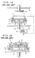
- Figs. 1A and 1B show schematically the structure of a prior art, planar magnetron sputtering apparatus.
- a target plate (referred to hereinafter merely as a target) 1 is backed up at its rear surface by a backing plate 2.
- a peripheral annular magnetic pole member 4 and a central solid cylindrical magnetic pole member 5 Disposed on the rear surface side of the backing plate 2 are a peripheral annular magnetic pole member 4 and a central solid cylindrical magnetic pole member 5 which are magnetically coupled to each other by a yoke 3 to constitute a magnetic circuit.
- the target 1 and the backing plate 2 are made of non-magnetic materials respectively, and the lines of magnetic flux flowing between the magnetic members draw an arc extending through the target 1 in the thicknesswise direction of the target 1 as shown in Fig. 1B.
- a cathode 6 encloses the magnetic members 4, 5 and yoke 3 therein and is hermetically closed by the backing plate 2.
- a shield 8 is mounted on the outer peripheral portion of the cathode 6 with an annular insulating member 7 interposed therebetween.
- the cathode 6 is supported on a shaft 10 which is electrically insulated from and hermetically secured to a hermetic or vacuum enclosure wall 9 of a vacuum chamber.
- An anode 11 is disposed above the cathode 6, and a power source 12 is connected between the anode 11 and the cathode 6.
- the lines of magnetic force in the vicinity of the surface of the target 1 are distributed to provide a doughnut-like or semi-annular magnetic field distribution 13 as best seen in Fig. 1B.
- Application of the power supply voltage across the anode 11 and the cathode 6 generates plasma.
- the semi-annular magnetic field distribution 13 acts to confine the plasma so that the plasma has a high density in a toroidal ring region 14 shown in Fig. 1B.
- the ions in the plasma are accelerated by an electric field substantially perpendicular to the surface of the target 1 to impinge against the surface of the target 1.
- the constituent atoms or particles are sputtered out from the surface of the target 1 to leave a locally eroded or etched region 15 on the target surface.
- the atoms or particles sputtered out from the surface of the target 1 migrate toward and onto the lower surface of a substrate 17 supported on a substrate stage 16 to deposit and form a thin film on the lower surface of the substrate 17.
- the eroded or etched region 15 on the surface of the target 1 is progressively widened with time due to repetition of the sputtering process.
- this erosion is generally limited to a specific region on the surface of the target 1 in the target arrangement shown in Fig. 1B.
- the plasma has a high density above a limited region only of the surface of the target 1, and progressive erosion of the target 1 due to repeated sputtering is limited to a specific region only of the target 1. Because of the limited small area of the source of sputtering, the rate of deposition of the target material on the substrate 17 cannot be increased, and the rate of utilization of the target surface is also low.
- the present invention eliminates the use of the magnets disposed beneath the target in the electrode structure of the prior art magnetron sputtering apparatus and yet attains the formation of high-density plasma over a wide area of the surface of the target. More precisely, according to the present invention, high-density plasma covering a substantial area of the surface of the target is generated without resorting to the use of a magnetic field forming a closed loop of magnetic flux extending through the target in the thicknesswise direction of the target.
- Plasma having a high density is generated with the use of a magnetic field not forming a closed loop inside the electrode structure which contains the target, unlike the prior art, and the plasma is maintained above the target to cover a wide area of the surface of the target for effecting desired sputtering.
- magnets for establishing a mirror magnetic field are disposed at a place remote from a target, and microwaves are introduced toward and into the space defined by the lines of magnetic force of the mirror magnetic field thereby generating plasma having a high density.
- the space defined by the magnetic lines of force of the mirror magnetic field (the intermediate bulged portion of the magnetic flux) exhibits a confinement effect on the plasma.
- the electrode structure in the present invention includes an anode and a cathode (a power source is to be connected therebetween), and a target is supported on the cathode. Therefore, an electric field substantially perpendicular to the surface of the target is produced. Cations existing above the target are accelerated by the electric field to impinge against the target.
- the absence of any magnetic lines of force forming a closed loop in the electrode structure which contains the target is equivalent to or indicates the absence of a magnetic flux distribution drawing an arc above the target and having a bulged portion extending adjacent to a limited region only of the target. Therefore, a limited region only of the target is not eroded unlike that employed in the prior art sputtering apparatus of the planar magnetron type.
- the high-density plasma is generated by the aid of the mirror magnetic field, but the plasma is not localized to a limited region only of the target.
- the high-density plasma is maintained in an area above the target according to, for example, one of the following manners: (1) The high-density plasma is generated at a place distant from the target by the combination of a mirror magnetic field and microwaves, and the thus generated high-density plasma is guided to migrate toward an area above the target. (2) Plasma migrated according to the method (1) is confined in a magnetic field whose lines of force do not penetrate the target and are in parallel to the surface of the target. (3) A mirror magnetic field is established in an area close to the target in such a relation that the lines of force or magnetic flux penetrate the entire surface of the target, and microwaves are directed toward and into the space defined by the mirror magnetic field.
- Figs. 2 and 3 show an embodiment of the present invention in which plasma having a high density is generated in a plasma generating section and is then guided to migrate toward an area above a target disposed in a processing chamber.
- a plasma generating section A includes a pair of magnets 41, 42 for establishing a mirror magnetic field and a source 35 of microwaves.
- the mirror magnetic field is established by the magnets 41 and 42, and microwaves from the microwave source 35 are directed toward and into the chamber 37 in a relation coaxial with the mirror magnetic field.
- the microwave source 35 supplies the microwaves through a waveguide 36.
- microwaves is used to designate electromagnetic waves having a wavelength less than about 100 cm.
- electromagnetic waves having a wavelength of from about 1 cm to about 100 cm are called the microwaves.
- a microwave source of 2.45 GHz (corresponding to a wavelength of about 12 cm) is well known.
- the plasma generating chamber 37 is a waveguide in itself and hermetically communicates with a processing section B through an opening 34 to form a hermetic structure.
- the plasma generating chamber 37 is connected to the waveguide 36 for the microwave source 35 through a hermetically sealed microwave window 39 formed of a material such as quartz or alumina and through a tapered waveguide 38 tapered for the purpose of diameter matching.
- the plasma generating chamber 37 is provided with a gas inlet 40 through which a plasma-forming gas, for example, an inert gas such as Ar, Xe, He or Rn can be introduced.
- a plasma-forming gas for example, an inert gas such as Ar, Xe, He or Rn can be introduced.
- Ar or Xe is used.
- a processing chamber (described later) enclosed by a hermetic or vacuum enclosure wall 29 can be evacuated together with the plasma generating chamber 37 by an evacuating system including, for example, a cryopanel maintained at the temperature of liquid He and aided by a rotary pump, or a turbo-molecular pump.
- the vacuum is desirably oil-less and clean.
- a working gas such as Ar at a pressure of the order of 10 ⁇ 4 to 10 ⁇ 2 Torr (10 ⁇ 2 to 100 Pa) is introduced into the plasma generating chamber 37 from the gas inlet 40, and the microwaves from the microwave source 35 are directed to the working gas to generate plasma in the chamber 37.
- the microwave source 35 is a 2.45 GHz source
- the upper limit of the density of the plasma is usually 7.4 ⁇ 1010 electrons/c.c. without the aid of a magnetic field. It is to be noted that the above limit is exceeded by the utilization of a magnetic field, and plasma having a high density can be generated.
- a mirror magnetic field having a strength exceeding that required for satisfying the condition of electron cyclotron resonance (ECR) is established in parallel to the direction of the microwaves, the cut-off condition disappears, and plasma having a density as high as 1011 to 1012 electrons/c.c. can be generated.
- the pair of electromagnets 41 and 42 are provided for establishing such a mirror magnetic field, and the magnet 42 has a field strength higher than that of the magnet 41. Therefore, rightward migration of the plasma in Fig. 2 is restricted, and the plasma migrates in the direction of from the magnet 42 toward the magnet 41 (leftward in Fig. 2).
- the processing section B includes an evacuatable processing chamber enclosed by the wall 29, and, in this evacuatable processing chamber, a substrate 31 to be deposited with a thin film is disposed opposite to a target 21 made of a film-forming material and contained in an electrode structure 33.
- the substrate 31 is held in position by a substrate holder 32, and the holder 32 is supported by a supporting shaft 24. Both of the holder 32 and the shaft 24 are made of a metal material.
- the shaft 24 is hermetically fixed in position in a relation electrically insulated from the chamber wall 29.
- the electrode structure 33 is supported on a feed through post 28 which is hermetically fixed in position in a relation electrically insulated from the chamber wall 29.
- the substrate 31 may be disposed in any suitable position relative to the target 21, provided that the material sputtered out from the target 21 can be successfully deposited in thin film form on the surface of the substrate 31.
- both of the target 21 and the substrate 31 extend vertically and are disposed opposite to each other as shown.
- the electrode structure 33 does not include magnets unlike that in the prior art sputtering apparatus of the planar magnetron type.
- a cathode 23 is disposed beneath the target 21 with a backing plate 22 made of a good electrical and thermal conductor such as copper interposed therebetween, and an anode 27 is disposed around the stack of the target 21, backing plate 22 and cathode 23 with insulator members 25 and 26 interposed therebetween, so that cations can be directed perpendicularly toward and onto the surface of the target 21.
- Both of the anode 27 and the cathode 23 may be formed of a metal such as a stainless steel or aluminum.
- the target 21 is formed of a material to be deposited on the surface of the substrate 31.
- Typical examples of the material of the target 21 are a metal such as Al, W or Mo, a semiconductor such as Si, and an electrical insulator such as SiO2.
- a power source 30, e.g. a DC power source is shown connected between the anode 27 and the cathode 23 for establishing a cation-accelerating electric field above the target 21.
- an rf source is connected between the anode 27 and the cathode 23.
- the upper end of the opening 34 lies beneath the substrate 31, and its center lies above the target 21. This is because, when a portion of the opening 34 lies above the substrate 31, trouble such as etching of the substrate 31 and the film deposited thereon tends to occur, while, when the center of the opening 34 lies beneath the target 21, the highest density portion of the plasma can be hardly effectively utilized.
- the central axis of the plasma generating chamber 37 makes an angle with the surface of the target 21, it is preferable that an extension of the central axis of the chamber 37 intersects with the middle portion of the surface of the target 21.
- the DC power source 30 is described as an example of the cation-accelerating power source, it may be replaced by an rf power source.
- the rf power source is effective for preventing charge-up of the target 21.
- Other charge-up preventive means or charge neutralizing means may be combined with the power source when so desired.
- the process of deposition of a film on the substrate 31 by sputtering includes introducing, for example, Ar gas into the plasma generating chamber 37 (and the processing chamber 29) until a predetermined pressure builds up, energizing the electromagnets 41, 42 and directing the microwaves from the microwave source 35 toward and into the plasma generating chamber 37. Consequently, plasma having a high density (1011 to 1012 electrons/c.c.) is generated in the space defined principally by the mirror magnetic field in the plasma generating chamber 37. Since the strength of the right-hand portion of the mirror magnetic field is larger than that of the left-hand portion in Fig. 2, the substantial portion of the plasma diffuses leftward to migrate into the processing chamber 29.
- the plasma migrated into the processing chamber 29 diffuses over a wide area of the surface of the target 21 to cause sputtering of the material of the target 21 under influence of the electric field established in a relation substantially perpendicular to the surface of the target 21. Atoms, molecules, etc. sputtered out from the surface of the target 21 fly upward to be deposited on the surface of the substrate 31.
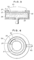
- Fig. 3 shows schematically the profile of the plasma 43 maintained above the target 21.
- This plasma 43 is generated in the plasma generating chamber 37 and guided to migrate toward the area above the target 21.
- the magnets disposed beneath the target in the prior art apparatus are removed, and plasma formed at a separate place is guided to migrate toward the area above the target 21. Therefore, the high-density plasma can be distributed over a wide area above the surface of the target 21, and no hollow portion occurs in the plasma unlike the prior art, planar magnetron sputtering.
- the wide area (preferably, the entire area) of the surface of the target 21 can participate in the sputtering operation.
- the quantity of atoms or particles sputtered out from the surface of the target 21 per unit time increases, and the rate of deposition of the atoms or particles on the surface of the substrate 31 also increases. Further, almost the entirety of the surface area of the target 21 is eroded to greatly increase the rate of the usable area of the target 21, and this increases the number of wafers that can be processed with a single target.
- the density of high-density plasma can be controlled by controlling the microwave source 35, and the power supply voltage applied across the anode 27 and the cathode 23 provides the ion-accelerating energy.
- the density of the plasma and the acceleration of the ions can be controlled independently, so that the optimized sputtering conditions meeting the material of the target can be selected as desired.
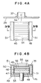
- Figs. 4A and 4B show part of another embodiment of the present invention which comprises an electrode structure exhibiting a marked confining effect on electrons in plasma guided to migrate toward the area above a target.
- the Lorentz's force produced by a magnetic field is imparted to electrons migrating toward a target from a plasma generating chamber to impart rotary motion to the electrons for trapping the electrons in the vicinity of the surface of the target.
- a magnetic field substantially parallel to the surface of the target is established.
- the structure of this second embodiment is generally similar to that of the first embodiment shown in and described with reference to Fig. 2, except its electrode structure.
- a cathode 47, a backing plate 46 and a target plate 45 are stacked in tiers to constitute a cathode structure, as in the case of Fig. 2. It will be seen in Fig. 4A that this cathode structure is rectangular in shape. This rectangular shape is advantageous over a circular shape in that a uniform magnetic field parallel to the surface of a target can more easily be produced.
- An insulator member 48 surrounds the cathode structure, and an anode structure 52 surrounds the insulator member 48.
- the anode structure 52 includes an anode base 49 and magnetic members 50, 51 disposed on the bath end edge portions respectively of the anode base 49.
- a yoke 53 magnetically coupling the magnetic members 50 and 51 is disposed between the anode base 49 and the insulator member 48.
- the yoke 53 and the magnetic members 50, 51 are magnetically coupled to constitute a magnetic circuit which is open at its upper part. By the function of this magnetic circuit, a magnetic flux distribution 54 substantially parallel to the surface of a target 45 is provided above the target 45.
- Fig. 4A electrons migrating from the plasma generating chamber 37 cross the magnetic field 54.
- the electrons are subjected to rotary motion by the Lorentz's force.
- the electrons imparted with the rotary motion are trapped in an area in the vicinity of the target 45.
- the trapped electrons impinge against neutral molecules/atoms to further promote ionization thereby maintaining the plasma at the high density.
- the high-density plasma 55 (Fig. 4B) is maintained above the surface of the target 45.
- the cations in the high-density plasma 55 are accelerated by an electric field substantially perpendicular to the surface of the target 45 to impinge against the surface of the target 45 thereby causing sputtering of atoms or particles from the surface of the target 45. These atoms or molecules deposit on the surface of a substrate (not shown) to form a thin film thereon.
- the target 45 is eroded over a widely extended region in the second embodiment of the present invention until finally the target 45 can be eroded over its entire surface region.
- the plasma maintained above the target 45 has a density higher than that in the first embodiment shown in Fig. 2, by virtue of the plasma confining effect of the magnetic field. Therefore, the film deposition by sputtering can be attained at a higher rate. Further, due to the fact that the plasma can be confined in the area adjacent to the target 45, close access of the plasma to the substrate can be prevented, thereby reducing the possibility of impingement of charged particles against the substrate and minimizing damage to the substrate.
- Figs. 5 and 6 show still another embodiment of the present invention in which a mirror magnetic field is formed directly above a target, and microwaves are directed toward plasma for attaining sputtering by erosion of a widest possible area of the surface of the target.
- this third embodiment its electrode structure and substrate supporting structure are similar to those employed in the embodiment shown in Fig. 2.
- a target 21 is backed up at its rear surface by a backing plate 22, and a cathode 23 is disposed to make intimate engagement at its front surface with the rear surface of the backing plate 22.
- An anode 27 is disposed outside of the cathode 23 with a disc-shaped insulator member 25 and a cylindrical insulator member 26 interposed therebetween.
- a feed through post 28 of the cathode 23 extends through a vacuum enclosure wall 29 to support the anode 27 and cathode 23 in an evacuatable processing chamber in a relation electrically insulated from the wall 29.
- a power source 30 is connected between the anode 27 and the cathode 23.
- a substrate 31 is disposed on a substrate holder 32 at a position opposite to the target 21.
- a shaft 24 of the substrate holder 32 extends through the vacuum enclosure wall 29 to support the substrate 31 in the evacuatable processing chamber in a relation electrically insulated from the wall 29.
- An opening 34 is provided in a portion of a vacuum enclosure wall 57 surrounding the electrode structure 33, and a waveguide 60 for microwaves is connected at one end thereof to the opening 34.
- Another waveguide 36 is connected at one end thereof to the other end of the waveguide 60 through a hermetic window 39 permeable to microwaves and at the other end thereof to a microwave source 35.
- the waveguides 36 and 60 are so disposed as to direct microwaves toward an area above the surface of the target 21.
- the window 39 is disposed at a position retracted or spaced apart from the wall 29 of the processing chamber so that the sputtered material may not deposit on the window 39 thereby obstruct introduction of the microwaves.
- the microwave introduction mechanism may be any other suitable one, provided that microwaves can be effectively directed toward the area above the target 21, and deposition of the sputtered material on the window 39 can be prevented. Although only one microwave introduction mechanism is illustrated, a plurality of such mechanisms may be disposed in radial relation.
- the axis of the microwave introduction system is arranged to be horizontal, and the lower end of the waveguide 60 aligns substantially with the upper end of the electrode structure 33, as illustrated.
- the upper limit of the density of the plasma is 7.4 ⁇ 1010 electrons/c.c. at the most.
- plasma will diffuse, and it will be unable to increase the density of the plasma in the area above the target. Therefore, a magnetic field having a strength exceeding that required for satisfying the condition of ECR is produced above the target 21.
- the target 21 and the vacuum enclosure wall 57 are preferably circular in sectional shape for producing such a magnetic flux distribution.
- annular magnets 58 and 59 are disposed outside the vacuum enclosure wall 57 at position upper and lower relative to the waveguide 60. These magnets 58 and 59 establish a mirror magnetic field so that charged particles (especially, electrons having high energy) in the plasma generated in the vicinity of the electrode structure 33 can be confined in an area near the surface of the target 21 and may not impinge against the substrate 31.
- the working gas may be introduced from any desired position provided that it can be quickly supplied toward and onto the target 21.
- it is most effective to introduce the microwaves in a relation coaxial with the axis of the magnetic field.
- the microwaves are introduced along the surface of the target 21 as shown in Fig. 5.
- the power supply voltage from the power source 30 is applied across the anode 27 and the cathode 23, and the microwaves from the microwave source 35 are introduced to generate the plasma in the area above the target 21. Electrons in the plasma are excited by the microwaves in the mirror magnetic field established by the magnets 58 and 59, thereby making cyclotron motion. Consequently, impingement between the electrons and the neutral particles is promoted to increase the density of the plasma.
- plasma having a high density is formed above the surface of the target 21.
- plasma having a controlled high density covering the entire area of the surface of the target 21 can be generated as in the case of Fig. 3.
- the ions in the plasma are accelerated to migrate toward and onto the surface of the target 21 under influence of the electric field substantially perpendicular to the target surface until the ions impinge against the surface of the target 21.
- constituent atoms or particles are sputtered out from the surface of the target 21, and the thus sputtered-out atoms or particles deposit to form a thin film on the surface of the substrate 31.
- the plasma formed in the area above the surface of the target 21 has a high density over the entire area of the surface of the target 21. Therefore, almost the entirety of the surface of the target 21 can be eroded as a result of sputtering.
- plasma having a high density can be generated in the area above the entire surface of the target 21, and almost the entirety of the surface of the target 21 can participate in the sputtering operation. Therefore, the quantity of atoms or particles sputtered out from the surface of the target 21 per unit time increases, and the rate of deposition of the atoms or particles on the surface of the substrate 31 also increases. Further, almost the entirety of the surface area of the target 21 is eroded to greatly increase the rate of the usable area of the target 21, and this increases the number of wafers that can be processed with a single target.
- the density of high-density plasma can be controlled by controlling the microwave source, and the power supply voltage applied across the anode 27 and the cathode 23 provides the ion-accelerating electric field.
- the density of the plasma and the acceleration of the ions can be controlled independently, so that the optimized sputtering conditions meeting the material of the target can be selected as desired.
Landscapes
- Chemical & Material Sciences (AREA)
- Engineering & Computer Science (AREA)
- Physics & Mathematics (AREA)
- Plasma & Fusion (AREA)
- Analytical Chemistry (AREA)
- Materials Engineering (AREA)
- Chemical Kinetics & Catalysis (AREA)
- Mechanical Engineering (AREA)
- Metallurgy (AREA)
- Organic Chemistry (AREA)
- Physical Vapour Deposition (AREA)
- Physical Deposition Of Substances That Are Components Of Semiconductor Devices (AREA)
- Plasma Technology (AREA)
Claims (21)
- Procédé de pulvérisation comprenant les étapes consistant à- disposer une structure d'électrode (33; 47, 52) portant une cible plane (21; 45) en face d'un substrat (31), ladite cible plane étant placée sous une pression prédéterminée dans une chambre de traitement (29) et une surface de ladite cible plane se trouvant en vis-à-vis dudit substrat,- provoquer la pulvérisation d'un matériau cible depuis ladite cible (21; 45) par l'action d'un plasma en vue du dépôt d'une pellicule mince sur la surface dudit substrat (31),- maintenir ledit plasma à une densité élevée dans une zone au-dessus de ladite surface de ladite cible (21; 45) en utilisant des champs magnétiques créés par des aimants (41, 42; 58, 59) et des micro-ondes qui sont introduites depuis une direction le long de ladite surface de ladite cible, et- accélérer les ions dudit plasma vers et sur la surface de ladite cible (21; 45) par l'action d'un champ électrique établi par ladite structure d'électrode (33; 47, 52) pour provoquer une choc des ions contre la surface de ladite cible, en provoquant ainsi ladite pulvérisation dudit matériau cible depuis ladite cible en vue du dépôt dudit film mince sur la surface dudit substrat (31),ledit procédé étant caractérisé en ce qu'il comporte en outre les étapes consistant à- disposer une paire d'aimants (41, 42; 58, 59) à l'extérieur de ladite structure d'électrode (33; 47, 52) de manière à créer un champ magnétique miroir et a diriger des micro-ondes vers et dans l'espace défini par ledit champ magnétique miroir, en générant ainsi ledit plasma à haute densité dans ledit espace,- guider ledit plasma à densité élevée pour l'amener a migrer depuis l'endroit où il est produit vers un espace large au-dessus de ladite cible (21; 45),
et- pulvériser ladite cible (21; 45) à l'aide dudit plasma à densité élevée dans ledit espace large de manière à pulvériser ladite cible (21; 45) dans une région large de ladite surface de ladite cible. - Procédé selon la revendication 1, caractérisé en ce que ledit champ magnétique miroir possède des lignes magnétiques de force d'une configuration couvrant ladite cible (21) pour emprisonner des électrons dans une zone proche de ladite cible.
- Procédé selon la revendication 1 ou 2, caractérisé en ce que les lignes magnétiques de force dudit champ magnétique miroir ne forment pas sensiblement une boucle fermée à l'intérieur de ladite structure d'électrode (33) portant ladite cible (21).
- Procédé selon la revendication 1, caractérisé en ce que ledit champ magnétique miroir est formé dans une chambre de génération de plasma (37) disposée adjacente à une chambre de traitement (29) dans laquelle sont placés ladite structure d'électrode (33) et ledit substrat (31).
- Procédé selon la revendication 4, caractérisé en ce que ladite chambre de génération de plasma (37) comprend une ouverture (34) ouverte vers un point au-dessus de ladite cible (21) et communique avec une source de micro-ondes (35) à travers une fenêtre perméable aux microondes (39) disposée entre ladite paire d'aimants (41, 42) créant ledit champ magnétique miroir.
- Procédé selon la revendication 5, caractérisé en ce que ledit champ magnétique possède une intensité supérieure à la valeur nécessaire pour satisfaire la condition de résonance cyclotron électronique des micro-ondes utilisées, ladite intensité étant plus grande sur le côté de ladite fenêtre (39) que sur le côté de ladite ouverture (34).
- Procédé selon la revendication 6, caractérisé en ce qu'il comporte en outre l'étape consistant à générer un champ magnétique le long de la surface de ladite cible (45) pour accélérer la migration des électrons vers ladite cible et piéger lesdits électrons dans une zone proche de ladite cible.
- Procédé selon la revendication 6 ou 7, caractérisé en ce que l'axe de ladite chambre de génération de plasma (37) s'étend horizontalement et court au-dessus de ladite cible (21).
- Procédé selon la revendication 1, caractérisé en ce que ledit espace est défini à proximité de la surface de ladite cible (21)
et
en ce que ladite paire d'aimants (58, 59) pour générer ledit champ magnétique miroir sont disposés autour de ladite chambre de traitement (29) contenant ladite structure d'électrode (33) et ledit substrat (31) à l'intérieur. - Dispositif de pulvérisation comprenant- une structure d'électrode (33; 47, 52) portant une cible plane (21; 45),- une structure (32) supportant un substrat (31) en face de ladite cible (21)
et- des moyens pour générer un plasma à haute densité pour provoquer une pulvérisation du matériau cible depuis ladite cible (21) en vue du dépôt d'un film mince sur la surface dudit substrat (31),caractérisé en ce que ledit dispositif comporte en outre- une paire d'aimants (41, 42; 58, 59) disposés en un emplacement écarté de ladite structure d'électrode (33; 47, 52) pour établir un champ magnétique miroir définissant un espace créant un plasma a haute densité et- une source de micro-ondes (35) dirigeant des micro-ondes vers et dans l'espace créant un plasma à haute densité dans une direction parallèle à la surface de ladite cible (21) et le long de la surface de ladite cible (21), ledit champ magnétique miroir et ladite source de micro-ondes (35) agissant en combinaison pour créer le plasma à haute densité au-dessus de la cible (21) sur une large zone superficielle de celle-ci. - Dispositif de pulvérisation selon la revendication 10, caractérisé en ce que ledit espace générant un plasma à haute densité est défini dans une zone proche de la surface de ladite cible (21) et en ce que ladite paire d'aimants (41, 42; 58, 59) sont espacés dans la direction de la normale au centre de ladite cible (21) coaxialement à ladite normale.
- Dispositif de pulvérisation selon la revendication 10, caractérisé en ce que ledit champ magnétique miroir possède une intensité supérieure à celle nécessaire pour satisfaire la condition de résonance cyclotron électronique desdites micro-ondes.
- Dispositif de pulvérisation selon la revendication 10, caractérisé en ce que ledit espace créant un plasma à haute densité est défini en un emplacement éloigné de ladite structure d'électrode (33) et en ce que ladite paire d'aimants (41, 42) et ladite source de micro-ondes (35) sont disposées autour dudit espace créant le plasma à haute densité de sorte que ledit champ magnétique miroir soit sensiblement coaxial aux micro-ondes.
- Dispositif de pulvérisation selon la revendication 11, caractérisé en ce que ladite source de micro-ondes (35) est disposée de manière à diriger les micro-ondes vers une position au-dessus de ladite cible (21) et le long de la surface de celle-ci.
- Dispositif de pulvérisation selon la revendication 13, caractérisé en ce que ledit espace générant le plasma à haute densité est défini dans un guide d'ondes (37) ayant une ouverture (34) ouverte vers ladite cible (21).
- Dispositif de pulvérisation selon la revendication 15, caractérisé en ce que ladite paire d'aimants (41, 42) est disposée selon le sens longitudinal dudit guide d'ondes (37) coaxialement à celui-ci et en ce que l'aimant (42) qui est plus éloigné de ladite cible (21) crée un champ magnétique d'intensité supérieure à celui créé par l'aimant (41) qui est plus proche de ladite cible (21).
- Dispositif de pulvérisation selon la revendication 16, caractérisé en ce que ladite cible (21) est disposée horizontalement et en ce que ledit guide d'ondes (37) également disposé horizontalement a son extrémité supérieure plus basse que la surface dudit substrat (31) et son axe central plus haut que la surface de ladite cible (21).
- Dispositif de pulvérisation selon la revendication 16 ou 17, caractérisé en ce que ledit guide d'ondes (37) a son axe central s'étendant sensiblement vers une zone au-dessus de ladite cible (21).
- Dispositif de pulvérisation selon la revendication 17, caractérisé en ce que ladite structure d'électrode comprend une cathode (47) disposée au-dessous de ladite cible (21) et une paire d'aimants (50, 51) disposés sur les deux côtés opposés de ladite cible (21), ladite paire d'aimants créant un champ magnétique qui est sensiblement parallèle à la surface de ladite cible (21) et est dirigé de sorte que les électrons migrant à travers ledit guide d'ondes (37) sont soumis à un mouvement rotatif.
- Dispositif de pulvérisation à source d'énergie micro-ondes, comportant une cathode et un porte-substrat, ladite cathode étant agencée pour retenir une cible plane constituée d'un matériau à pulvériser, le porte-substrat étant agencé pour supporter un substrat d'une manière à se trouver en face de ladite cible et- une fenêtre d'introduction de plasma, une source d'énergie micro-ondes, ladite source d'énergie micro-ondes étant apte à délivrer des micro-ondes dans une direction parallèle à la surface de ladite cible plane, et des aimants éloignés de ladite cathode pour créer un plasma en combinaison avec ladite source d'énergie micro-ondes pour pulvériser ladite cible, lesdits aimants étant aptes à créer un champ magnétique qui transfère latéralement ledit plasma dans un espace entre ladite cible et ledit porte-substrat.
- Dispositif de pulvérisation selon la revendication 20, caractérisé en ce que lesdites micro-ondes sont introduites par l'intermédiaire de ladite fenêtre depuis une direction parallèle à la surface de ladite cible dans l'espace entre ladite cible et ledit porte-substrat et en ce que lesdits aimants sont disposés à l'extérieur et entourent une chambre dans laquelle sont disposés ladite cathode et ledit porte-substrat, lesdits aimants générant un champ magnétique de manière à produire un plasma en combinaison avec lesdites micro-ondes introduites dans ledit champ magnétique et lesdits aimants confinant ledit plasma à proximité de ladite surface de ladite cible.
Applications Claiming Priority (2)
| Application Number | Priority Date | Filing Date | Title |
|---|---|---|---|
| JP243870/83 | 1983-12-26 | ||
| JP58243870A JPH0627323B2 (ja) | 1983-12-26 | 1983-12-26 | スパツタリング方法及びその装置 |
Publications (4)
| Publication Number | Publication Date |
|---|---|
| EP0148504A2 EP0148504A2 (fr) | 1985-07-17 |
| EP0148504A3 EP0148504A3 (en) | 1987-10-07 |
| EP0148504B1 EP0148504B1 (fr) | 1990-11-22 |
| EP0148504B2 true EP0148504B2 (fr) | 1995-07-12 |
Family
ID=17110200
Family Applications (1)
| Application Number | Title | Priority Date | Filing Date |
|---|---|---|---|
| EP84116391A Expired - Lifetime EP0148504B2 (fr) | 1983-12-26 | 1984-12-27 | Procédé et appareil de pulvérisation |
Country Status (5)
| Country | Link |
|---|---|
| US (1) | US4610770A (fr) |
| EP (1) | EP0148504B2 (fr) |
| JP (1) | JPH0627323B2 (fr) |
| KR (1) | KR890004880B1 (fr) |
| DE (1) | DE3483647D1 (fr) |
Families Citing this family (61)
| Publication number | Priority date | Publication date | Assignee | Title |
|---|---|---|---|---|
| JPH0627323B2 (ja) | 1983-12-26 | 1994-04-13 | 株式会社日立製作所 | スパツタリング方法及びその装置 |
| JPS6113626A (ja) * | 1984-06-29 | 1986-01-21 | Hitachi Ltd | プラズマ処理装置 |
| EP0173164B1 (fr) * | 1984-08-31 | 1988-11-09 | Hitachi, Ltd. | Vaporisation à l'aide de micro-ondes |
| US4842707A (en) * | 1986-06-23 | 1989-06-27 | Oki Electric Industry Co., Ltd. | Dry process apparatus |
| JPS6324030A (ja) * | 1986-06-26 | 1988-02-01 | Res Dev Corp Of Japan | 異方性希土類磁石材料およびその製造方法 |
| JPS6376867A (ja) * | 1986-09-19 | 1988-04-07 | Mitsubishi Kasei Corp | 反応性スパツタリング装置 |
| JP2587924B2 (ja) * | 1986-10-11 | 1997-03-05 | 日本電信電話株式会社 | 薄膜形成装置 |
| JP2631650B2 (ja) * | 1986-12-05 | 1997-07-16 | アネルバ株式会社 | 真空装置 |
| JPH066786B2 (ja) * | 1987-03-17 | 1994-01-26 | 日本電信電話株式会社 | 薄膜形成装置 |
| US4834860A (en) * | 1987-07-01 | 1989-05-30 | The Boc Group, Inc. | Magnetron sputtering targets |
| DE3803355A1 (de) * | 1988-02-05 | 1989-08-17 | Leybold Ag | Teilchenquelle fuer eine reaktive ionenstrahlaetz- oder plasmadepositionsanlage |
| US5125358A (en) * | 1988-07-26 | 1992-06-30 | Matsushita Electric Industrial Co., Ltd. | Microwave plasma film deposition system |
| US5180436A (en) * | 1988-07-26 | 1993-01-19 | Matsushita Electric Industrial Co., Ltd. | Microwave plasma film deposition system |
| US4952273A (en) * | 1988-09-21 | 1990-08-28 | Microscience, Inc. | Plasma generation in electron cyclotron resonance |
| JPH0689446B2 (ja) * | 1988-12-19 | 1994-11-09 | 株式会社日立製作所 | 薄膜形成装置 |
| JP2934711B2 (ja) * | 1989-12-07 | 1999-08-16 | カシオ計算機株式会社 | スパッタ装置 |
| US5045166A (en) * | 1990-05-21 | 1991-09-03 | Mcnc | Magnetron method and apparatus for producing high density ionic gas discharge |
| US5707692A (en) * | 1990-10-23 | 1998-01-13 | Canon Kabushiki Kaisha | Apparatus and method for processing a base substance using plasma and a magnetic field |
| ATE147890T1 (de) * | 1991-05-31 | 1997-02-15 | Deposition Sciences Inc | Sputteranlage |
| DE4119362A1 (de) * | 1991-06-12 | 1992-12-17 | Leybold Ag | Teilchenquelle, insbesondere fuer reaktive ionenaetz- und plasmaunterstuetzte cvd-verfahren |
| US5490910A (en) * | 1992-03-09 | 1996-02-13 | Tulip Memory Systems, Inc. | Circularly symmetric sputtering apparatus with hollow-cathode plasma devices |
| JPH06192830A (ja) * | 1992-07-31 | 1994-07-12 | Texas Instr Inc <Ti> | 材料層の物理的蒸気沈着のための方法と装置 |
| DE4230290A1 (de) * | 1992-09-10 | 1994-03-17 | Leybold Ag | Vorrichtung zum Erzeugen eines Plasmas mittels Kathodenzerstäubung und Mikrowelleneinstrahlung |
| DE4230291C2 (de) * | 1992-09-10 | 1999-11-04 | Leybold Ag | Mikrowellenunterstützte Zerstäubungsanordnung |
| DE4336830A1 (de) * | 1993-10-28 | 1995-05-04 | Leybold Ag | Plasma-Zerstäubungsanlage mit Mikrowellenunterstützung |
| KR100226366B1 (ko) * | 1995-08-23 | 1999-10-15 | 아끼구사 나오유끼 | 플라즈마장치 및 플라즈마 처리방법 |
| US5855745A (en) * | 1997-04-23 | 1999-01-05 | Sierra Applied Sciences, Inc. | Plasma processing system utilizing combined anode/ ion source |
| JP3944946B2 (ja) * | 1997-04-25 | 2007-07-18 | 株式会社島津製作所 | 薄膜形成装置 |
| FR2774251B1 (fr) * | 1998-01-26 | 2000-02-25 | Commissariat Energie Atomique | Source a plasma micro-onde lineaire en aimants permanents |
| KR100422184B1 (ko) * | 2001-11-10 | 2004-03-11 | 아이티엠 주식회사 | 진공 아크를 이용한 고품위 박막 형성 방법 |
| US8500973B2 (en) * | 2004-08-20 | 2013-08-06 | Jds Uniphase Corporation | Anode for sputter coating |
| US7879209B2 (en) * | 2004-08-20 | 2011-02-01 | Jds Uniphase Corporation | Cathode for sputter coating |
| US7658802B2 (en) * | 2005-11-22 | 2010-02-09 | Applied Materials, Inc. | Apparatus and a method for cleaning a dielectric film |
| US8268116B2 (en) * | 2007-06-14 | 2012-09-18 | Lam Research Corporation | Methods of and apparatus for protecting a region of process exclusion adjacent to a region of process performance in a process chamber |
| WO2013170052A1 (fr) | 2012-05-09 | 2013-11-14 | Sio2 Medical Products, Inc. | Enrobage protecteur en saccharide pour conditionnement pharmaceutique |
| MX350703B (es) | 2009-05-13 | 2017-09-14 | Sio2 Medical Products Inc | Metodo de gasificacion para inspeccionar una superficie revestida. |
| US9458536B2 (en) | 2009-07-02 | 2016-10-04 | Sio2 Medical Products, Inc. | PECVD coating methods for capped syringes, cartridges and other articles |
| US11624115B2 (en) | 2010-05-12 | 2023-04-11 | Sio2 Medical Products, Inc. | Syringe with PECVD lubrication |
| US9878101B2 (en) | 2010-11-12 | 2018-01-30 | Sio2 Medical Products, Inc. | Cyclic olefin polymer vessels and vessel coating methods |
| US9272095B2 (en) | 2011-04-01 | 2016-03-01 | Sio2 Medical Products, Inc. | Vessels, contact surfaces, and coating and inspection apparatus and methods |
| CN103262663B (zh) | 2011-04-28 | 2016-12-14 | 住友理工株式会社 | 微波等离子体生成装置和采用该装置的磁控溅射成膜装置 |
| EP2776603B1 (fr) | 2011-11-11 | 2019-03-06 | SiO2 Medical Products, Inc. | Revêtement de passivation, de protection de ph ou à pouvoir lubrifiant pour conditionnement pharmaceutique, processus et appareil de revêtement |
| US11116695B2 (en) | 2011-11-11 | 2021-09-14 | Sio2 Medical Products, Inc. | Blood sample collection tube |
| JP5907701B2 (ja) * | 2011-11-18 | 2016-04-26 | 住友理工株式会社 | フィルム部材の製造方法 |
| US20150297800A1 (en) | 2012-07-03 | 2015-10-22 | Sio2 Medical Products, Inc. | SiOx BARRIER FOR PHARMACEUTICAL PACKAGE AND COATING PROCESS |
| US9184030B2 (en) | 2012-07-19 | 2015-11-10 | Lam Research Corporation | Edge exclusion control with adjustable plasma exclusion zone ring |
| FR2995493B1 (fr) * | 2012-09-11 | 2014-08-22 | Hydromecanique & Frottement | Dispositif pour generer un plasma presentant une etendue importante le long d'un axe par resonnance cyclotronique electronique rce a partir d'un milieu gazeux |
| CA2890066C (fr) | 2012-11-01 | 2021-11-09 | Sio2 Medical Products, Inc. | Procedes d'inspection de revetement |
| US9903782B2 (en) | 2012-11-16 | 2018-02-27 | Sio2 Medical Products, Inc. | Method and apparatus for detecting rapid barrier coating integrity characteristics |
| US9764093B2 (en) | 2012-11-30 | 2017-09-19 | Sio2 Medical Products, Inc. | Controlling the uniformity of PECVD deposition |
| JP6382830B2 (ja) | 2012-11-30 | 2018-08-29 | エスアイオーツー・メディカル・プロダクツ・インコーポレイテッド | 医療シリンジ、カートリッジ等上でのpecvd堆積の均一性制御 |
| US9662450B2 (en) | 2013-03-01 | 2017-05-30 | Sio2 Medical Products, Inc. | Plasma or CVD pre-treatment for lubricated pharmaceutical package, coating process and apparatus |
| EP2971228B1 (fr) | 2013-03-11 | 2023-06-21 | Si02 Medical Products, Inc. | Emballage revêtu |
| US9937099B2 (en) | 2013-03-11 | 2018-04-10 | Sio2 Medical Products, Inc. | Trilayer coated pharmaceutical packaging with low oxygen transmission rate |
| US20160017490A1 (en) | 2013-03-15 | 2016-01-21 | Sio2 Medical Products, Inc. | Coating method |
| WO2015148471A1 (fr) | 2014-03-28 | 2015-10-01 | Sio2 Medical Products, Inc. | Revêtements antistatiques pour des récipients en plastique |
| CN103966567B (zh) * | 2014-05-05 | 2016-03-16 | 京东方科技集团股份有限公司 | 一种平面靶材的磁场结构及其使用方法 |
| EP3337915B1 (fr) | 2015-08-18 | 2021-11-03 | SiO2 Medical Products, Inc. | Conditionnement pharmaceutique et autre présentant un faible taux de transmission d'oxygène |
| FR3042797B1 (fr) * | 2015-10-27 | 2021-01-22 | Commissariat Energie Atomique | Dispositif pour la fabrication d'une couche en carbone amorphe par plasma a la resonance cyclotron electronique |
| JP7138504B2 (ja) * | 2018-07-31 | 2022-09-16 | キヤノントッキ株式会社 | 成膜装置及び電子デバイスの製造方法 |
| CN113774342A (zh) * | 2020-06-09 | 2021-12-10 | 江苏菲沃泰纳米科技股份有限公司 | 溅射镀膜设备及其电极装置和镀膜方法 |
Citations (1)
| Publication number | Priority date | Publication date | Assignee | Title |
|---|---|---|---|---|
| EP0148504B1 (fr) † | 1983-12-26 | 1990-11-22 | Hitachi, Ltd. | Procédé et appareil de pulvérisation |
Family Cites Families (10)
| Publication number | Priority date | Publication date | Assignee | Title |
|---|---|---|---|---|
| US3325394A (en) * | 1963-07-01 | 1967-06-13 | Ibm | Magnetic control of film deposition |
| FR2324755A1 (fr) * | 1975-09-19 | 1977-04-15 | Anvar | Dispositif de pulverisation cathodique de grande vitesse de depot |
| JPS55131175A (en) * | 1979-03-30 | 1980-10-11 | Toshiba Corp | Surface treatment apparatus with microwave plasma |
| JPS5613480A (en) * | 1979-07-13 | 1981-02-09 | Hitachi Ltd | Dry etching apparatus |
| JPS5673539A (en) * | 1979-11-22 | 1981-06-18 | Toshiba Corp | Surface treating apparatus of microwave plasma |
| JPS5779621A (en) * | 1980-11-05 | 1982-05-18 | Mitsubishi Electric Corp | Plasma processing device |
| JPS5875839A (ja) * | 1981-10-30 | 1983-05-07 | Fujitsu Ltd | スパツタ装置 |
| JPS58161774A (ja) * | 1982-03-17 | 1983-09-26 | Fujitsu Ltd | スパツタリング処理方法 |
| EP0103461B1 (fr) * | 1982-09-10 | 1988-11-17 | Nippon Telegraph And Telephone Corporation | Appareil et procédé de dépôt à plasma |
| JPS6016424A (ja) * | 1983-07-08 | 1985-01-28 | Fujitsu Ltd | マイクロ波プラズマ処理方法及びその装置 |
-
1983
- 1983-12-26 JP JP58243870A patent/JPH0627323B2/ja not_active Expired - Lifetime
-
1984
- 1984-12-20 KR KR1019840008169A patent/KR890004880B1/ko not_active Expired
- 1984-12-24 US US06/686,005 patent/US4610770A/en not_active Expired - Lifetime
- 1984-12-27 DE DE8484116391T patent/DE3483647D1/de not_active Expired - Lifetime
- 1984-12-27 EP EP84116391A patent/EP0148504B2/fr not_active Expired - Lifetime
Patent Citations (1)
| Publication number | Priority date | Publication date | Assignee | Title |
|---|---|---|---|---|
| EP0148504B1 (fr) † | 1983-12-26 | 1990-11-22 | Hitachi, Ltd. | Procédé et appareil de pulvérisation |
Also Published As
| Publication number | Publication date |
|---|---|
| EP0148504A2 (fr) | 1985-07-17 |
| EP0148504A3 (en) | 1987-10-07 |
| JPS60135573A (ja) | 1985-07-18 |
| KR850005147A (ko) | 1985-08-21 |
| JPH0627323B2 (ja) | 1994-04-13 |
| DE3483647D1 (de) | 1991-01-03 |
| KR890004880B1 (ko) | 1989-11-30 |
| EP0148504B1 (fr) | 1990-11-22 |
| US4610770A (en) | 1986-09-09 |
Similar Documents
| Publication | Publication Date | Title |
|---|---|---|
| EP0148504B2 (fr) | Procédé et appareil de pulvérisation | |
| JP3020580B2 (ja) | マイクロ波プラズマ処理装置 | |
| KR100659828B1 (ko) | 이온화 물리적 증착 방법 및 장치 | |
| EP0300447B1 (fr) | Procédé et appareil pour traiter un matériau à l'aide de plasma | |
| EP1076911B1 (fr) | Procede et appareil de metallisation par depot sous vide de vapeur ionisee | |
| US5122252A (en) | Arrangement for the coating of substrates | |
| EP0283519B1 (fr) | Generateur ionique, installation de formation de films minces utilisant ce generateur et source d'ions | |
| EP0978138A1 (fr) | Procede et dispositif de pulverisation par bombardement ionique sur un materiau | |
| JPH06220631A (ja) | マイクロ波強化スパッタリング装置 | |
| US5804027A (en) | Apparatus for generating and utilizing magnetically neutral line discharge type plasma | |
| JP2552701B2 (ja) | イオン源 | |
| JP2674995B2 (ja) | 基板処理方法およびその装置 | |
| JPS6386864A (ja) | イオン源 | |
| JP2777657B2 (ja) | プラズマ付着装置 | |
| JPH02156526A (ja) | マイクロ波プラズマ処理装置 | |
| JPS6389663A (ja) | スパツタリング装置 | |
| JPH0578849A (ja) | 有磁場マイクロ波プラズマ処理装置 | |
| JP3100242B2 (ja) | プラズマ処理装置 | |
| JPH06140362A (ja) | プラズマ処理装置 | |
| JPH02197567A (ja) | プラズマスパッタ装置 | |
| JPS6396283A (ja) | イオン源 | |
| JP2832256B2 (ja) | プラズマ付着装置 | |
| JPS61114518A (ja) | プラズマ付着装置 | |
| JPH1092600A (ja) | プラズマ処理装置 | |
| JPH07258843A (ja) | スパッタ装置 |
Legal Events
| Date | Code | Title | Description |
|---|---|---|---|
| PUAI | Public reference made under article 153(3) epc to a published international application that has entered the european phase |
Free format text: ORIGINAL CODE: 0009012 |
|
| AK | Designated contracting states |
Designated state(s): DE FR GB |
|
| PUAL | Search report despatched |
Free format text: ORIGINAL CODE: 0009013 |
|
| AK | Designated contracting states |
Kind code of ref document: A3 Designated state(s): DE FR GB |
|
| 17P | Request for examination filed |
Effective date: 19871008 |
|
| 17Q | First examination report despatched |
Effective date: 19890706 |
|
| GRAA | (expected) grant |
Free format text: ORIGINAL CODE: 0009210 |
|
| AK | Designated contracting states |
Kind code of ref document: B1 Designated state(s): DE FR GB |
|
| REF | Corresponds to: |
Ref document number: 3483647 Country of ref document: DE Date of ref document: 19910103 |
|
| ET | Fr: translation filed | ||
| PLBI | Opposition filed |
Free format text: ORIGINAL CODE: 0009260 |
|
| 26 | Opposition filed |
Opponent name: LEYBOLD AKTIENGESELLSCHAFT Effective date: 19910205 |
|
| PUAH | Patent maintained in amended form |
Free format text: ORIGINAL CODE: 0009272 |
|
| STAA | Information on the status of an ep patent application or granted ep patent |
Free format text: STATUS: PATENT MAINTAINED AS AMENDED |
|
| 27A | Patent maintained in amended form |
Effective date: 19950712 |
|
| AK | Designated contracting states |
Kind code of ref document: B2 Designated state(s): DE FR GB |
|
| ET3 | Fr: translation filed ** decision concerning opposition | ||
| REG | Reference to a national code |
Ref country code: GB Ref legal event code: IF02 |
|
| PGFP | Annual fee paid to national office [announced via postgrant information from national office to epo] |
Ref country code: FR Payment date: 20031124 Year of fee payment: 20 |
|
| PGFP | Annual fee paid to national office [announced via postgrant information from national office to epo] |
Ref country code: GB Payment date: 20031126 Year of fee payment: 20 |
|
| PGFP | Annual fee paid to national office [announced via postgrant information from national office to epo] |
Ref country code: DE Payment date: 20031203 Year of fee payment: 20 |
|
| PG25 | Lapsed in a contracting state [announced via postgrant information from national office to epo] |
Ref country code: GB Free format text: LAPSE BECAUSE OF EXPIRATION OF PROTECTION Effective date: 20041226 |
|
| REG | Reference to a national code |
Ref country code: GB Ref legal event code: PE20 |