EP0148687B1 - Photoempfindliche Vorrichtung mit strahlungsundurchlässigen Zonen zwischen den Detektoren und Herstellungsverfahren - Google Patents
Photoempfindliche Vorrichtung mit strahlungsundurchlässigen Zonen zwischen den Detektoren und Herstellungsverfahren Download PDFInfo
- Publication number
- EP0148687B1 EP0148687B1 EP84402637A EP84402637A EP0148687B1 EP 0148687 B1 EP0148687 B1 EP 0148687B1 EP 84402637 A EP84402637 A EP 84402637A EP 84402637 A EP84402637 A EP 84402637A EP 0148687 B1 EP0148687 B1 EP 0148687B1
- Authority
- EP
- European Patent Office
- Prior art keywords
- layer
- opaque
- radiation
- metal
- detected
- Prior art date
- Legal status (The legal status is an assumption and is not a legal conclusion. Google has not performed a legal analysis and makes no representation as to the accuracy of the status listed.)
- Expired
Links
- 230000005855 radiation Effects 0.000 title claims description 30
- 238000004519 manufacturing process Methods 0.000 title claims description 5
- 238000000034 method Methods 0.000 title claims 7
- 239000000758 substrate Substances 0.000 claims description 24
- 229910052751 metal Inorganic materials 0.000 claims description 20
- 239000002184 metal Substances 0.000 claims description 20
- 239000010407 anodic oxide Substances 0.000 claims description 10
- 238000000151 deposition Methods 0.000 claims description 6
- 230000008021 deposition Effects 0.000 claims description 6
- PCHJSUWPFVWCPO-UHFFFAOYSA-N gold Chemical compound [Au] PCHJSUWPFVWCPO-UHFFFAOYSA-N 0.000 claims description 5
- 229910052737 gold Inorganic materials 0.000 claims description 5
- 239000010931 gold Substances 0.000 claims description 5
- 239000011347 resin Substances 0.000 claims description 5
- 229920005989 resin Polymers 0.000 claims description 5
- PXHVJJICTQNCMI-UHFFFAOYSA-N Nickel Chemical compound [Ni] PXHVJJICTQNCMI-UHFFFAOYSA-N 0.000 claims description 4
- 239000003989 dielectric material Substances 0.000 claims description 4
- 238000001704 evaporation Methods 0.000 claims description 4
- 230000008020 evaporation Effects 0.000 claims description 4
- WPYVAWXEWQSOGY-UHFFFAOYSA-N indium antimonide Chemical compound [Sb]#[In] WPYVAWXEWQSOGY-UHFFFAOYSA-N 0.000 claims description 4
- 229910052782 aluminium Inorganic materials 0.000 claims description 3
- XAGFODPZIPBFFR-UHFFFAOYSA-N aluminium Chemical compound [Al] XAGFODPZIPBFFR-UHFFFAOYSA-N 0.000 claims description 3
- 239000000463 material Substances 0.000 claims description 3
- 230000003647 oxidation Effects 0.000 claims description 3
- 238000007254 oxidation reaction Methods 0.000 claims description 3
- JBRZTFJDHDCESZ-UHFFFAOYSA-N AsGa Chemical compound [As]#[Ga] JBRZTFJDHDCESZ-UHFFFAOYSA-N 0.000 claims description 2
- VYZAMTAEIAYCRO-UHFFFAOYSA-N Chromium Chemical compound [Cr] VYZAMTAEIAYCRO-UHFFFAOYSA-N 0.000 claims description 2
- 229910001218 Gallium arsenide Inorganic materials 0.000 claims description 2
- GPXJNWSHGFTCBW-UHFFFAOYSA-N Indium phosphide Chemical compound [In]#P GPXJNWSHGFTCBW-UHFFFAOYSA-N 0.000 claims description 2
- RTAQQCXQSZGOHL-UHFFFAOYSA-N Titanium Chemical compound [Ti] RTAQQCXQSZGOHL-UHFFFAOYSA-N 0.000 claims description 2
- 238000005119 centrifugation Methods 0.000 claims description 2
- 229910052804 chromium Inorganic materials 0.000 claims description 2
- 239000011651 chromium Substances 0.000 claims description 2
- 150000001875 compounds Chemical class 0.000 claims description 2
- 229910052759 nickel Inorganic materials 0.000 claims description 2
- OCGWQDWYSQAFTO-UHFFFAOYSA-N tellanylidenelead Chemical compound [Pb]=[Te] OCGWQDWYSQAFTO-UHFFFAOYSA-N 0.000 claims description 2
- 229910052719 titanium Inorganic materials 0.000 claims description 2
- 239000010936 titanium Substances 0.000 claims description 2
- 238000010298 pulverizing process Methods 0.000 claims 2
- UGFAIRIUMAVXCW-UHFFFAOYSA-N Carbon monoxide Chemical compound [O+]#[C-] UGFAIRIUMAVXCW-UHFFFAOYSA-N 0.000 claims 1
- XUIMIQQOPSSXEZ-UHFFFAOYSA-N Silicon Chemical compound [Si] XUIMIQQOPSSXEZ-UHFFFAOYSA-N 0.000 claims 1
- 239000004411 aluminium Substances 0.000 claims 1
- 238000007598 dipping method Methods 0.000 claims 1
- 150000002500 ions Chemical class 0.000 claims 1
- WYUZTTNXJUJWQQ-UHFFFAOYSA-N tin telluride Chemical compound [Te]=[Sn] WYUZTTNXJUJWQQ-UHFFFAOYSA-N 0.000 claims 1
- 239000004065 semiconductor Substances 0.000 description 11
- 230000000694 effects Effects 0.000 description 5
- 229910003437 indium oxide Inorganic materials 0.000 description 3
- PJXISJQVUVHSOJ-UHFFFAOYSA-N indium(iii) oxide Chemical class [O-2].[O-2].[O-2].[In+3].[In+3] PJXISJQVUVHSOJ-UHFFFAOYSA-N 0.000 description 3
- 230000015556 catabolic process Effects 0.000 description 2
- 238000009792 diffusion process Methods 0.000 description 2
- -1 ln Sb Substances 0.000 description 2
- 238000000206 photolithography Methods 0.000 description 2
- LIVNPJMFVYWSIS-UHFFFAOYSA-N silicon monoxide Chemical compound [Si-]#[O+] LIVNPJMFVYWSIS-UHFFFAOYSA-N 0.000 description 2
- 238000004544 sputter deposition Methods 0.000 description 2
- 238000007738 vacuum evaporation Methods 0.000 description 2
- MARUHZGHZWCEQU-UHFFFAOYSA-N 5-phenyl-2h-tetrazole Chemical compound C1=CC=CC=C1C1=NNN=N1 MARUHZGHZWCEQU-UHFFFAOYSA-N 0.000 description 1
- ZOKXTWBITQBERF-UHFFFAOYSA-N Molybdenum Chemical compound [Mo] ZOKXTWBITQBERF-UHFFFAOYSA-N 0.000 description 1
- KWYUFKZDYYNOTN-UHFFFAOYSA-M Potassium hydroxide Chemical compound [OH-].[K+] KWYUFKZDYYNOTN-UHFFFAOYSA-M 0.000 description 1
- ATJFFYVFTNAWJD-UHFFFAOYSA-N Tin Chemical compound [Sn] ATJFFYVFTNAWJD-UHFFFAOYSA-N 0.000 description 1
- 240000008042 Zea mays Species 0.000 description 1
- FYEOSUFWPIXZOR-UHFFFAOYSA-N [bis(selanylidene)-$l^{5}-arsanyl]selanyl-bis(selanylidene)-$l^{5}-arsane Chemical compound [Se]=[As](=[Se])[Se][As](=[Se])=[Se] FYEOSUFWPIXZOR-UHFFFAOYSA-N 0.000 description 1
- 238000010521 absorption reaction Methods 0.000 description 1
- 239000000969 carrier Substances 0.000 description 1
- 210000004027 cell Anatomy 0.000 description 1
- 230000008878 coupling Effects 0.000 description 1
- 238000010168 coupling process Methods 0.000 description 1
- 238000005859 coupling reaction Methods 0.000 description 1
- 238000005868 electrolysis reaction Methods 0.000 description 1
- 229910052738 indium Inorganic materials 0.000 description 1
- APFVFJFRJDLVQX-UHFFFAOYSA-N indium atom Chemical compound [In] APFVFJFRJDLVQX-UHFFFAOYSA-N 0.000 description 1
- 230000006698 induction Effects 0.000 description 1
- 239000011810 insulating material Substances 0.000 description 1
- QSHDDOUJBYECFT-UHFFFAOYSA-N mercury Chemical compound [Hg] QSHDDOUJBYECFT-UHFFFAOYSA-N 0.000 description 1
- 229910052753 mercury Inorganic materials 0.000 description 1
- 150000002739 metals Chemical class 0.000 description 1
- 229910052750 molybdenum Inorganic materials 0.000 description 1
- 239000011733 molybdenum Substances 0.000 description 1
- 230000003287 optical effect Effects 0.000 description 1
- BASFCYQUMIYNBI-UHFFFAOYSA-N platinum Chemical compound [Pt] BASFCYQUMIYNBI-UHFFFAOYSA-N 0.000 description 1
- 230000035945 sensitivity Effects 0.000 description 1
- 230000006641 stabilisation Effects 0.000 description 1
- 238000011105 stabilization Methods 0.000 description 1
- 229910052714 tellurium Inorganic materials 0.000 description 1
- PORWMNRCUJJQNO-UHFFFAOYSA-N tellurium atom Chemical compound [Te] PORWMNRCUJJQNO-UHFFFAOYSA-N 0.000 description 1
Images
Classifications
-
- H—ELECTRICITY
- H10—SEMICONDUCTOR DEVICES; ELECTRIC SOLID-STATE DEVICES NOT OTHERWISE PROVIDED FOR
- H10F—INORGANIC SEMICONDUCTOR DEVICES SENSITIVE TO INFRARED RADIATION, LIGHT, ELECTROMAGNETIC RADIATION OF SHORTER WAVELENGTH OR CORPUSCULAR RADIATION
- H10F39/00—Integrated devices, or assemblies of multiple devices, comprising at least one element covered by group H10F30/00, e.g. radiation detectors comprising photodiode arrays
- H10F39/10—Integrated devices
- H10F39/107—Integrated devices having multiple elements covered by H10F30/00 in a repetitive configuration, e.g. radiation detectors comprising photodiode arrays
-
- H—ELECTRICITY
- H10—SEMICONDUCTOR DEVICES; ELECTRIC SOLID-STATE DEVICES NOT OTHERWISE PROVIDED FOR
- H10F—INORGANIC SEMICONDUCTOR DEVICES SENSITIVE TO INFRARED RADIATION, LIGHT, ELECTROMAGNETIC RADIATION OF SHORTER WAVELENGTH OR CORPUSCULAR RADIATION
- H10F39/00—Integrated devices, or assemblies of multiple devices, comprising at least one element covered by group H10F30/00, e.g. radiation detectors comprising photodiode arrays
- H10F39/10—Integrated devices
- H10F39/12—Image sensors
- H10F39/18—Complementary metal-oxide-semiconductor [CMOS] image sensors; Photodiode array image sensors
- H10F39/184—Infrared image sensors
-
- H—ELECTRICITY
- H10—SEMICONDUCTOR DEVICES; ELECTRIC SOLID-STATE DEVICES NOT OTHERWISE PROVIDED FOR
- H10F—INORGANIC SEMICONDUCTOR DEVICES SENSITIVE TO INFRARED RADIATION, LIGHT, ELECTROMAGNETIC RADIATION OF SHORTER WAVELENGTH OR CORPUSCULAR RADIATION
- H10F77/00—Constructional details of devices covered by this subclass
- H10F77/30—Coatings
- H10F77/306—Coatings for devices having potential barriers
- H10F77/331—Coatings for devices having potential barriers for filtering or shielding light, e.g. multicolour filters for photodetectors
- H10F77/334—Coatings for devices having potential barriers for filtering or shielding light, e.g. multicolour filters for photodetectors for shielding light, e.g. light blocking layers or cold shields for infrared detectors
-
- Y—GENERAL TAGGING OF NEW TECHNOLOGICAL DEVELOPMENTS; GENERAL TAGGING OF CROSS-SECTIONAL TECHNOLOGIES SPANNING OVER SEVERAL SECTIONS OF THE IPC; TECHNICAL SUBJECTS COVERED BY FORMER USPC CROSS-REFERENCE ART COLLECTIONS [XRACs] AND DIGESTS
- Y10—TECHNICAL SUBJECTS COVERED BY FORMER USPC
- Y10S—TECHNICAL SUBJECTS COVERED BY FORMER USPC CROSS-REFERENCE ART COLLECTIONS [XRACs] AND DIGESTS
- Y10S148/00—Metal treatment
- Y10S148/118—Oxide films
-
- Y—GENERAL TAGGING OF NEW TECHNOLOGICAL DEVELOPMENTS; GENERAL TAGGING OF CROSS-SECTIONAL TECHNOLOGIES SPANNING OVER SEVERAL SECTIONS OF THE IPC; TECHNICAL SUBJECTS COVERED BY FORMER USPC CROSS-REFERENCE ART COLLECTIONS [XRACs] AND DIGESTS
- Y10—TECHNICAL SUBJECTS COVERED BY FORMER USPC
- Y10S—TECHNICAL SUBJECTS COVERED BY FORMER USPC CROSS-REFERENCE ART COLLECTIONS [XRACs] AND DIGESTS
- Y10S257/00—Active solid-state devices, e.g. transistors, solid-state diodes
- Y10S257/906—Dram with capacitor electrodes used for accessing, e.g. bit line is capacitor plate
Definitions
- the present invention relates to a photosensitive device comprising between the detectors areas opaque to the radiation to be detected. It also relates to a method of manufacturing such a device.
- the detectors in question are generally photo-diodes or photo-MOS, integrated in the same semiconductor substrate.
- This "edge effect” manifests itself in particular in semiconductor substrates sensitive to infrared radiation. It is either binary materials such as indium antimonide, ln Sb, lead tellurium, Pb Te ..., or ternary materials such as mercury and cadmium telluride, Cd Hg Te or tin and lead telluride, Pb Sn Te.
- This "edge effect” is observed more generally when a semiconductor substrate with high mobility is used; this is the case for example of semiconductors, consisting of compounds of the families Ili and V, such as gallium arsenide, As Ga, or indium phosphide, P In.
- junctions are made in the semiconductor substrate which is covered with oxide. Through windows pierced through the oxide, electrodes are deposited in contact with the substrate. These electrodes are subjected to a potential and at the same time their geometry determines that of the zones opaque to the radiation separating the detectors.
- the present invention relates to a photosensitive device comprising between the detectors of the areas opaque to radiation which eliminates the drawbacks, of solutions known from the prior art.
- the device according to the invention is not obtained by self-indexing as is the case for the device of application EP-A-0 024 970.
- the invention makes it possible to vary the surface of the photosensitive detectors without difficulty.
- a first layer of anodic oxide covering the entire semiconductor substrate allows perfect stabilization of the photo-voltaic junctions. This is due to the qualities specific to anodic oxides; in particular, a thin oxide layer, around 10 to 60 nm (100 to 600 A), for example, is sufficient to obtain these results.
- the device according to the invention it is possible without difficulty to cover the edges of the junctions, since the first insulating layer extends over the entire substrate and the second layer, opaque to the radiation to be detected, is etched by photo-lithography, which allows you to freely choose the areas where you want to keep this second layer.
- the second metal layer receives no voltage and is covered by an insulating layer.
- an avahtage of the device according to the invention is that the areas opaque to radiation have an insulating surface which can be used without risk of short circuit for the passage of various connections.
- the device according to the invention makes it possible to bring two photodiodes 50 ⁇ m apart from each other without too much intermodulation problem, whereas in the prior art at least 100 are required. ⁇ m.
- These figures correspond to the example of a semiconductor substrate of indium antimonide, type N, placed at 77 degrees Kelvin, comprising 5.10 15 carriers of majority charges per cubic centimeter, for which the lifetime of the holes is approximately 2.10- 7 seconds, their mobility is approximately 4000 cm 2 per Volt and per second, which corresponds to a diffusion coefficient of approximately 26 cm 2 per second and to a diffusion length Lp of approximately 23 ⁇ m.
- the same example for a P type indium antimonide substrate shows that at a distance of 60 ⁇ m from the edge of a junction, the signal is practically zero.
- the device according to the invention makes it possible in this case to bring two photo-diodes of approximately 15 ⁇ m closer to each other.
- the device according to the invention therefore makes it possible to increase the resolution by bringing the detectors closer together, while limiting the optical coupling between the detectors.
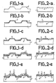
- FIGS. 1a to e and 2a to e represent various stages of a manufacturing process d 'An embodiment of a device according to the invention, in the case of a mesa structure in Figures 1a to e and das the case of a planar structure in Figures 2a to e.
- FIGS. 1a to e various stages of a method of manufacturing an embodiment of a device according to the invention have been shown.
- Photovoltaic junctions 2, of N / P or P / N type are symbolically represented in FIG. 1a by dotted lines on a semiconductor substrate 1.
- FIG. 1a diodes of the mesa type are shown.
- An oxide is grown by anodic oxidation over the entire surface of the substrate - see Figure 1b.
- This first layer of oxide bears the reference 3. Its thickness is approximately 10 to 60 nm (100 to 600 A).
- the growth of anodic oxide takes place, for example, by electrolysis.
- a semiconductor substrate made of indium atimoniide it is possible, for example, to immerse the substrate in a potassium hydroxide solution of which it constitutes the anode, while as cathode, a platinum wire is used for example.
- the oxide obtained is rich in indium oxides. It should be noted that the analysis of the product obtained reveals that the oxide deposition was carried out by anodic oxidation.
- indium oxide deposited by evaporation is conductive while anodic indium oxide is a very good dielectric.
- a second layer 4 opaque to the radiation to be detected is then deposited on the first layer of anode oxide 3 - see FIG. 1c.
- this second layer is not necessarily metallic.
- a body such as arsenic pentaselenide, A S2 Ses, is opaque to visible radiation.
- the second layer must be metallic, it may for example be made of gold or aluminum.
- a second layer 4 can be used, constituted by the superposition of at least first and second elementary metal layers.
- the first elementary metalic layer consists of a metal ensuring good contact, good "bonding", with the anodic oxide layer and with the second elementary metal layer.
- the second layer 4 opaque to the radiation to be detected can be formed by the superposition of several elementary layers.
- This second layer 4 is etched by photo-lithography for example, so as to cover only the areas which it is desired to make opaque to the radiation to be detected.
- Layer 4 can only be left between the detectors. It can also be left to extend over part of the detectors.
- This second layer has a thickness of about 100 to 600 nm (1000 to 6000 A) for example. It can be deposited for example by vacuum evaporation or sputtering.
- a third layer 5 - see FIG. 1d - is deposited in dielectric material, which covers the entire surface. It can be an organic isolate or not, for example negative photosensitive resin or silicon monoxide, Si 0.
- This last layer can be deposited for example by vacuum evaporation, cathode sputtering, ionic deposition, dip induction, centrifugation ...
- Its thickness can be, for example, of the order duum.
- metallic connections 6 can be made in contact with the junctions 2 through windows passing through the first and third layers. These connections 6 are arranged on the third layer 5. It is possible to use metal connections opaque to the radiation to be detected and which therefore modify the geometry of the photosensitive zones.
- Figures 2a to e differ from Figures 1a to e only because they show diodes with planar structure.
Landscapes
- Light Receiving Elements (AREA)
- Solid State Image Pick-Up Elements (AREA)
- Transforming Light Signals Into Electric Signals (AREA)
- Measurement Of Radiation (AREA)
Claims (14)
Applications Claiming Priority (2)
| Application Number | Priority Date | Filing Date | Title |
|---|---|---|---|
| FR8320842 | 1983-12-27 | ||
| FR8320842A FR2557371B1 (fr) | 1983-12-27 | 1983-12-27 | Dispositif photosensible comportant entre les detecteurs des zones opaques au rayonnement a detecter, et procede de fabrication |
Publications (2)
| Publication Number | Publication Date |
|---|---|
| EP0148687A1 EP0148687A1 (de) | 1985-07-17 |
| EP0148687B1 true EP0148687B1 (de) | 1988-02-03 |
Family
ID=9295601
Family Applications (1)
| Application Number | Title | Priority Date | Filing Date |
|---|---|---|---|
| EP84402637A Expired EP0148687B1 (de) | 1983-12-27 | 1984-12-18 | Photoempfindliche Vorrichtung mit strahlungsundurchlässigen Zonen zwischen den Detektoren und Herstellungsverfahren |
Country Status (5)
| Country | Link |
|---|---|
| US (1) | US4665609A (de) |
| EP (1) | EP0148687B1 (de) |
| JP (1) | JPH0652785B2 (de) |
| DE (1) | DE3469247D1 (de) |
| FR (1) | FR2557371B1 (de) |
Cited By (17)
| Publication number | Priority date | Publication date | Assignee | Title |
|---|---|---|---|---|
| US7027863B1 (en) | 1999-10-25 | 2006-04-11 | Impulse Dynamics N.V. | Device for cardiac therapy |
| US7062318B2 (en) | 1996-01-08 | 2006-06-13 | Impulse Dynamics (Israel) Ltd | Electrical muscle controller |
| US7167748B2 (en) | 1996-01-08 | 2007-01-23 | Impulse Dynamics Nv | Electrical muscle controller |
| US7460907B1 (en) | 1998-07-20 | 2008-12-02 | Impulse Dynamics N.V. | Pacing with hemodynamic enhancement |
| US7647102B2 (en) | 1999-10-25 | 2010-01-12 | Impulse Dynamics N.V. | Cardiac contractility modulation device having anti-arrhythmic capabilities and method of operating thereof |
| US7840262B2 (en) | 2003-03-10 | 2010-11-23 | Impulse Dynamics Nv | Apparatus and method for delivering electrical signals to modify gene expression in cardiac tissue |
| US8228311B2 (en) | 2003-02-10 | 2012-07-24 | N-Trig Ltd. | Touch detection for a digitizer |
| US8244371B2 (en) | 2005-03-18 | 2012-08-14 | Metacure Limited | Pancreas lead |
| US8346363B2 (en) | 1999-03-05 | 2013-01-01 | Metacure Limited | Blood glucose level control |
| US8352031B2 (en) | 2004-03-10 | 2013-01-08 | Impulse Dynamics Nv | Protein activity modification |
| US8548583B2 (en) | 2004-03-10 | 2013-10-01 | Impulse Dynamics Nv | Protein activity modification |
| US8666495B2 (en) | 1999-03-05 | 2014-03-04 | Metacure Limited | Gastrointestinal methods and apparatus for use in treating disorders and controlling blood sugar |
| US8700161B2 (en) | 1999-03-05 | 2014-04-15 | Metacure Limited | Blood glucose level control |
| US8792985B2 (en) | 2003-07-21 | 2014-07-29 | Metacure Limited | Gastrointestinal methods and apparatus for use in treating disorders and controlling blood sugar |
| US8934975B2 (en) | 2010-02-01 | 2015-01-13 | Metacure Limited | Gastrointestinal electrical therapy |
| US9101765B2 (en) | 1999-03-05 | 2015-08-11 | Metacure Limited | Non-immediate effects of therapy |
| US9289618B1 (en) | 1996-01-08 | 2016-03-22 | Impulse Dynamics Nv | Electrical muscle controller |
Families Citing this family (13)
| Publication number | Priority date | Publication date | Assignee | Title |
|---|---|---|---|---|
| JPS62112382A (ja) * | 1985-11-12 | 1987-05-23 | Toshiba Corp | 半導体受光装置 |
| US4720627A (en) * | 1986-11-03 | 1988-01-19 | United States Of America As Represented By The Secretary Of The Air Force | Ion sensitive photodetector |
| JPH0391970A (ja) * | 1989-09-05 | 1991-04-17 | Hamamatsu Photonics Kk | 半導体受光素子とその製造方法 |
| US5126921A (en) * | 1990-07-06 | 1992-06-30 | Akira Fujishima | Electronic component and a method for manufacturing the same |
| US8321013B2 (en) | 1996-01-08 | 2012-11-27 | Impulse Dynamics, N.V. | Electrical muscle controller and pacing with hemodynamic enhancement |
| US9713723B2 (en) | 1996-01-11 | 2017-07-25 | Impulse Dynamics Nv | Signal delivery through the right ventricular septum |
| FR2758888B1 (fr) * | 1997-01-27 | 1999-04-23 | Thomson Csf | Procede de modelisation fine du fouillis de sol recu par un radar |
| DE19848460A1 (de) * | 1998-10-21 | 2000-05-04 | Micronas Intermetall Gmbh | Halbleiterbauelement und Verfahren zum Herstellen eines Halbleiterchips |
| EP1284781B1 (de) | 2000-05-04 | 2017-10-11 | Impulse Dynamics N.V. | Signalübertragung durch das rechtsventrikulare septum |
| US11439815B2 (en) | 2003-03-10 | 2022-09-13 | Impulse Dynamics Nv | Protein activity modification |
| US11779768B2 (en) | 2004-03-10 | 2023-10-10 | Impulse Dynamics Nv | Protein activity modification |
| EP1868679B1 (de) | 2005-02-17 | 2017-05-03 | MetaCure Limited | Nicht unmittelbare therapeutische wirkungen |
| FR2990562B1 (fr) * | 2012-05-09 | 2015-03-06 | Sagem Defense Securite | Procede de realisation d'un capteur infrarouge insb |
Family Cites Families (7)
| Publication number | Priority date | Publication date | Assignee | Title |
|---|---|---|---|---|
| US3483096A (en) * | 1968-04-25 | 1969-12-09 | Avco Corp | Process for making an indium antimonide infrared detector contact |
| JPS53114674A (en) * | 1977-03-16 | 1978-10-06 | Fujitsu Ltd | Manufacture for compound semiconductor device |
| FR2464563A1 (fr) * | 1979-08-31 | 1981-03-06 | Thomson Csf | Dispositif photodetecteur a semi-conducteur et procede de fabrication, et analyseur d'image comportant un tel dispositif |
| US4355456A (en) * | 1980-03-07 | 1982-10-26 | General Dynamics, Pomona Division | Process of fabricating a Schottky barrier photovoltaic detector |
| US4319258A (en) * | 1980-03-07 | 1982-03-09 | General Dynamics, Pomona Division | Schottky barrier photovoltaic detector |
| JPS5773970A (en) * | 1980-10-28 | 1982-05-08 | Seiko Epson Corp | Semiconductor device |
| JPS5843571A (ja) * | 1981-09-08 | 1983-03-14 | Toshiba Corp | カラ−用固体撮像装置 |
-
1983
- 1983-12-27 FR FR8320842A patent/FR2557371B1/fr not_active Expired
-
1984
- 1984-12-18 DE DE8484402637T patent/DE3469247D1/de not_active Expired
- 1984-12-18 EP EP84402637A patent/EP0148687B1/de not_active Expired
- 1984-12-21 US US06/684,469 patent/US4665609A/en not_active Expired - Fee Related
- 1984-12-27 JP JP59282134A patent/JPH0652785B2/ja not_active Expired - Lifetime
Cited By (21)
| Publication number | Priority date | Publication date | Assignee | Title |
|---|---|---|---|---|
| US8260416B2 (en) | 1996-01-08 | 2012-09-04 | Impulse Dynamics, N.V. | Electrical muscle controller |
| US7062318B2 (en) | 1996-01-08 | 2006-06-13 | Impulse Dynamics (Israel) Ltd | Electrical muscle controller |
| US7167748B2 (en) | 1996-01-08 | 2007-01-23 | Impulse Dynamics Nv | Electrical muscle controller |
| US9289618B1 (en) | 1996-01-08 | 2016-03-22 | Impulse Dynamics Nv | Electrical muscle controller |
| US8311629B2 (en) | 1996-01-08 | 2012-11-13 | Impulse Dynamics, N.V. | Electrical muscle controller |
| US8301247B2 (en) | 1996-01-08 | 2012-10-30 | Impulse Dynamics, N.V. | Electrical muscle controller |
| US7460907B1 (en) | 1998-07-20 | 2008-12-02 | Impulse Dynamics N.V. | Pacing with hemodynamic enhancement |
| US8666495B2 (en) | 1999-03-05 | 2014-03-04 | Metacure Limited | Gastrointestinal methods and apparatus for use in treating disorders and controlling blood sugar |
| US8700161B2 (en) | 1999-03-05 | 2014-04-15 | Metacure Limited | Blood glucose level control |
| US8346363B2 (en) | 1999-03-05 | 2013-01-01 | Metacure Limited | Blood glucose level control |
| US9101765B2 (en) | 1999-03-05 | 2015-08-11 | Metacure Limited | Non-immediate effects of therapy |
| US7647102B2 (en) | 1999-10-25 | 2010-01-12 | Impulse Dynamics N.V. | Cardiac contractility modulation device having anti-arrhythmic capabilities and method of operating thereof |
| US7027863B1 (en) | 1999-10-25 | 2006-04-11 | Impulse Dynamics N.V. | Device for cardiac therapy |
| US8228311B2 (en) | 2003-02-10 | 2012-07-24 | N-Trig Ltd. | Touch detection for a digitizer |
| US7840262B2 (en) | 2003-03-10 | 2010-11-23 | Impulse Dynamics Nv | Apparatus and method for delivering electrical signals to modify gene expression in cardiac tissue |
| US8326416B2 (en) | 2003-03-10 | 2012-12-04 | Impulse Dynamics Nv | Apparatus and method for delivering electrical signals to modify gene expression in cardiac tissue |
| US8792985B2 (en) | 2003-07-21 | 2014-07-29 | Metacure Limited | Gastrointestinal methods and apparatus for use in treating disorders and controlling blood sugar |
| US8548583B2 (en) | 2004-03-10 | 2013-10-01 | Impulse Dynamics Nv | Protein activity modification |
| US8352031B2 (en) | 2004-03-10 | 2013-01-08 | Impulse Dynamics Nv | Protein activity modification |
| US8244371B2 (en) | 2005-03-18 | 2012-08-14 | Metacure Limited | Pancreas lead |
| US8934975B2 (en) | 2010-02-01 | 2015-01-13 | Metacure Limited | Gastrointestinal electrical therapy |
Also Published As
| Publication number | Publication date |
|---|---|
| JPS60169166A (ja) | 1985-09-02 |
| US4665609A (en) | 1987-05-19 |
| EP0148687A1 (de) | 1985-07-17 |
| FR2557371B1 (fr) | 1987-01-16 |
| DE3469247D1 (en) | 1988-03-10 |
| FR2557371A1 (fr) | 1985-06-28 |
| JPH0652785B2 (ja) | 1994-07-06 |
Similar Documents
| Publication | Publication Date | Title |
|---|---|---|
| EP0148687B1 (de) | Photoempfindliche Vorrichtung mit strahlungsundurchlässigen Zonen zwischen den Detektoren und Herstellungsverfahren | |
| EP1583156B1 (de) | Ultraviolettdetektionssensor und Verfahren zu dessen Herstellung | |
| US4972244A (en) | Photodiode and photodiode array on a II-VI material and processes for the production thereof | |
| EP1516368B1 (de) | Abbildungsvorrichtung | |
| US9612263B2 (en) | Photoelectric conversion element, photoelectric conversion apparatus and solid-state imaging apparatus | |
| EP0036802B1 (de) | Verfahren zur Herstellung amorpher Halbleiter-Speicheranordnungen | |
| EP0229574B1 (de) | Photovoltaischer HgCdTe-Heteroübergang-Detektor und Verfahren zu seiner Herstellung | |
| EP0109865A1 (de) | Herstellungsverfahren von integrierten Schaltungen, die Gate-Isolator-Halbleiter-Elemente mit wenigstens zwei Gate-Ebenen enthalten | |
| EP0317024A1 (de) | Herstellungsverfahren eines integrierten Infrarot-Photodetektors | |
| JP2009070950A (ja) | 紫外線センサ | |
| JPH0671097B2 (ja) | カラ−センサ− | |
| JPS63116474A (ja) | アバランシエ光検知器 | |
| EP0144264A1 (de) | Indium-Antimonid-Photodiode und Verfahren zur Herstellung | |
| WO2005024897A2 (en) | Systems and methods having a metal-semiconductor-metal (msm) photodetector with buried oxide layer | |
| US4307319A (en) | Semiconductor layer of oxygen depletion type cerium oxide or lead oxide | |
| EP0024970A2 (de) | Verfahren zur Herstellung eines Halbleiter-Fotodetektors | |
| FR2849272A1 (fr) | Dispositif de detection photo-electrique et notamment de rayonnement x ou y | |
| JP2705594B2 (ja) | 赤外線検出素子 | |
| US5497029A (en) | Tin-indium antimonide infrared detector | |
| EP0354619A1 (de) | Bildaufnahmevorrichtung vom Halbbildübertragungstyp | |
| JPH09191123A (ja) | 化合物半導体受光装置 | |
| FR2545275A1 (fr) | Photodetecteur tandem | |
| EP0066480A1 (de) | Überlaufvorrichtung für lichtempfindliche ladungsgekoppelte Anordnung | |
| JPS639756B2 (de) | ||
| JPH0458560A (ja) | 光電変換素子 |
Legal Events
| Date | Code | Title | Description |
|---|---|---|---|
| PUAI | Public reference made under article 153(3) epc to a published international application that has entered the european phase |
Free format text: ORIGINAL CODE: 0009012 |
|
| AK | Designated contracting states |
Designated state(s): DE GB SE |
|
| 17P | Request for examination filed |
Effective date: 19850729 |
|
| 17Q | First examination report despatched |
Effective date: 19870310 |
|
| GRAA | (expected) grant |
Free format text: ORIGINAL CODE: 0009210 |
|
| AK | Designated contracting states |
Kind code of ref document: B1 Designated state(s): DE GB SE |
|
| REF | Corresponds to: |
Ref document number: 3469247 Country of ref document: DE Date of ref document: 19880310 |
|
| GBT | Gb: translation of ep patent filed (gb section 77(6)(a)/1977) | ||
| PLBE | No opposition filed within time limit |
Free format text: ORIGINAL CODE: 0009261 |
|
| STAA | Information on the status of an ep patent application or granted ep patent |
Free format text: STATUS: NO OPPOSITION FILED WITHIN TIME LIMIT |
|
| 26N | No opposition filed | ||
| EAL | Se: european patent in force in sweden |
Ref document number: 84402637.7 |
|
| PGFP | Annual fee paid to national office [announced via postgrant information from national office to epo] |
Ref country code: SE Payment date: 19971117 Year of fee payment: 14 Ref country code: GB Payment date: 19971117 Year of fee payment: 14 |
|
| PGFP | Annual fee paid to national office [announced via postgrant information from national office to epo] |
Ref country code: DE Payment date: 19971120 Year of fee payment: 14 |
|
| PG25 | Lapsed in a contracting state [announced via postgrant information from national office to epo] |
Ref country code: GB Free format text: LAPSE BECAUSE OF NON-PAYMENT OF DUE FEES Effective date: 19981218 |
|
| PG25 | Lapsed in a contracting state [announced via postgrant information from national office to epo] |
Ref country code: SE Free format text: LAPSE BECAUSE OF NON-PAYMENT OF DUE FEES Effective date: 19981219 |
|
| GBPC | Gb: european patent ceased through non-payment of renewal fee |
Effective date: 19981218 |
|
| PG25 | Lapsed in a contracting state [announced via postgrant information from national office to epo] |
Ref country code: DE Free format text: LAPSE BECAUSE OF NON-PAYMENT OF DUE FEES Effective date: 19991001 |