EP0149563A2 - Halbleiterlaser - Google Patents
Halbleiterlaser Download PDFInfo
- Publication number
- EP0149563A2 EP0149563A2 EP85300322A EP85300322A EP0149563A2 EP 0149563 A2 EP0149563 A2 EP 0149563A2 EP 85300322 A EP85300322 A EP 85300322A EP 85300322 A EP85300322 A EP 85300322A EP 0149563 A2 EP0149563 A2 EP 0149563A2
- Authority
- EP
- European Patent Office
- Prior art keywords
- semiconductor laser
- layer
- current blocking
- indent
- blocking layer
- Prior art date
- Legal status (The legal status is an assumption and is not a legal conclusion. Google has not performed a legal analysis and makes no representation as to the accuracy of the status listed.)
- Granted
Links
Images

Classifications
-
- H—ELECTRICITY
- H01—ELECTRIC ELEMENTS
- H01S—DEVICES USING THE PROCESS OF LIGHT AMPLIFICATION BY STIMULATED EMISSION OF RADIATION [LASER] TO AMPLIFY OR GENERATE LIGHT; DEVICES USING STIMULATED EMISSION OF ELECTROMAGNETIC RADIATION IN WAVE RANGES OTHER THAN OPTICAL
- H01S5/00—Semiconductor lasers
- H01S5/10—Construction or shape of the optical resonator, e.g. extended or external cavity, coupled cavities, bent-guide, varying width, thickness or composition of the active region
-
- H—ELECTRICITY
- H01—ELECTRIC ELEMENTS
- H01S—DEVICES USING THE PROCESS OF LIGHT AMPLIFICATION BY STIMULATED EMISSION OF RADIATION [LASER] TO AMPLIFY OR GENERATE LIGHT; DEVICES USING STIMULATED EMISSION OF ELECTROMAGNETIC RADIATION IN WAVE RANGES OTHER THAN OPTICAL
- H01S5/00—Semiconductor lasers
- H01S5/20—Structure or shape of the semiconductor body to guide the optical wave ; Confining structures perpendicular to the optical axis, e.g. index or gain guiding, stripe geometry, broad area lasers, gain tailoring, transverse or lateral reflectors, special cladding structures, MQW barrier reflection layers
- H01S5/22—Structure or shape of the semiconductor body to guide the optical wave ; Confining structures perpendicular to the optical axis, e.g. index or gain guiding, stripe geometry, broad area lasers, gain tailoring, transverse or lateral reflectors, special cladding structures, MQW barrier reflection layers having a ridge or stripe structure
- H01S5/223—Buried stripe structure
- H01S5/2232—Buried stripe structure with inner confining structure between the active layer and the lower electrode
-
- H—ELECTRICITY
- H01—ELECTRIC ELEMENTS
- H01S—DEVICES USING THE PROCESS OF LIGHT AMPLIFICATION BY STIMULATED EMISSION OF RADIATION [LASER] TO AMPLIFY OR GENERATE LIGHT; DEVICES USING STIMULATED EMISSION OF ELECTROMAGNETIC RADIATION IN WAVE RANGES OTHER THAN OPTICAL
- H01S2301/00—Functional characteristics
- H01S2301/18—Semiconductor lasers with special structural design for influencing the near- or far-field
-
- H—ELECTRICITY
- H01—ELECTRIC ELEMENTS
- H01S—DEVICES USING THE PROCESS OF LIGHT AMPLIFICATION BY STIMULATED EMISSION OF RADIATION [LASER] TO AMPLIFY OR GENERATE LIGHT; DEVICES USING STIMULATED EMISSION OF ELECTROMAGNETIC RADIATION IN WAVE RANGES OTHER THAN OPTICAL
- H01S2301/00—Functional characteristics
- H01S2301/18—Semiconductor lasers with special structural design for influencing the near- or far-field
- H01S2301/185—Semiconductor lasers with special structural design for influencing the near- or far-field for reduction of Astigmatism
-
- H—ELECTRICITY
- H01—ELECTRIC ELEMENTS
- H01S—DEVICES USING THE PROCESS OF LIGHT AMPLIFICATION BY STIMULATED EMISSION OF RADIATION [LASER] TO AMPLIFY OR GENERATE LIGHT; DEVICES USING STIMULATED EMISSION OF ELECTROMAGNETIC RADIATION IN WAVE RANGES OTHER THAN OPTICAL
- H01S5/00—Semiconductor lasers
- H01S5/20—Structure or shape of the semiconductor body to guide the optical wave ; Confining structures perpendicular to the optical axis, e.g. index or gain guiding, stripe geometry, broad area lasers, gain tailoring, transverse or lateral reflectors, special cladding structures, MQW barrier reflection layers
- H01S5/22—Structure or shape of the semiconductor body to guide the optical wave ; Confining structures perpendicular to the optical axis, e.g. index or gain guiding, stripe geometry, broad area lasers, gain tailoring, transverse or lateral reflectors, special cladding structures, MQW barrier reflection layers having a ridge or stripe structure
- H01S5/223—Buried stripe structure
- H01S5/2232—Buried stripe structure with inner confining structure between the active layer and the lower electrode
- H01S5/2234—Buried stripe structure with inner confining structure between the active layer and the lower electrode having a structured substrate surface
Definitions
- the present invention relates to a semiconductor laser structure which ensures stable operation of a semiconductor laser element.
- a semiconductor laser having an index guide structure has widely been used as a light source in an optical information processing system such as an information recording/drawing disc system.
- an optical information processing system such as an information recording/drawing disc system.
- the return beam creates an interference effect, thereby increasing noise components as shown in FIGURE 1.
- the semiconductor laser of the above-mentioned type is disposed in a high temperature ambience while maintaining the laser output intensity constant, noise components extremely increase above a certain temperature as shown in FIGURE 2.
- a current injection width namely a stripe width
- a current injection width is narrowed to about the length of the carrier diffusion in an active layer, that is, about 2 to 4 um so as to minimize the return beam noise and the mode competition noise.
- the laser beam distribution is determined by the gain distribution. Since the cavity volume is small, the spontaneous emission beam greatly influences on the laser mode. Further, the gain spectrum width is widened due to the high density current injection, and the laser emission is performed in the multi longitudinal mode, whereby the influence caused by the return beam and the mode competition effect caused by the temeparture rise are minimized.
- the near-field pattern changes due to the variation of the injection current, due to the secular change, or due to the return beam. Therefore, a stable coupling with an optical system is not ensured. Further, the astigmatism is considerably large and, therefore, a good coupling is not ensured with an optical system, especially with a lens system.
- an object of the present invention is to provide a semiconductor laser which minimizes an interference noise caused by a return beam.
- Another object of the present invention is to provide a semiconductor laser which minimizes a mode competition noise even at a considerably high temperature.
- Still another object of the present invention is to provide a semiconductor laser which ensures a stable transverse mode.
- an index guide structure is formed near the both cleaved facets of a laser oscillation cavity. That is, the index guide width is substantially equal to the current injection width near the both ends of a semiconductor laser element.
- a gain guide structure is formed at the center of the semiconductor laser element. That is, the index guide width is considerably wider than the current injection width near the center of the cavity.
- the semiconductor laser of the present invention emits the laser beam in the multiple longitudinal mode.
- the index guide structure formed at both ends of the element functions to minimize the return beam noise and the mode competition noise. Further, the near-field pattern is stable, and the astigmatism is small.
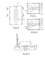
- FIGURES 3, 4 and 5 show an embodiment of a semiconductor laser of the present invention.
- a semiconductor laser of the present invention includes a p-GaAs substrate 1, and a current blocking layer 2 formed on the p-GaAs substrate 1.
- the current blocking layer 2 is made of an n-GaAs layer having a thickness of 0.6 to 1.5 pm.
- a V-shaped groove 3 is formed in the current blocking layer 2 to reach the p-GaAs substrate 1.
- An indent 4 having a width wider than the V-shaped groove 3 is formed near the center of the semiconductor laser before forming the V-shaped groove 3 in the current blocking layer 2.
- the indent 4 has a depth of about 0.1 to 0.2 pm so that the indent 4 does not reach the p-GaAs substrate 1, and the n-GaAs current blocking layer 2 has a thickness greater than 0.5 pm where the indent 4 is formed in the n-GaAs current blocking layer 2.
- the V-shaped groove 3 is formed in the n-GaAs current blocking layer 2 along the center line of the indent 4.
- a p-GaAIAs cladding layer 5, an n-GaAIAs active layer (or p-GaAIAs active layer) 6, an n-GaAlAs cladding layer 7, and an n-GaAs contacting layer 8 are sequentially formed on the n-GaAs current blocking layer 2 by the liquid phase epitaxial growth method so as to form the double hetero junction inner stripe semiconductor laser.
- the AlAs mole fraction of the cladding layers 5 and 7 is selected higher than that of the active layer 6 by 0.2 to 0.6.
- a Au-Ge-Ni ohmic n-side electrode 9 is formed on the n-GaAs contacting layer 8.
- a Au-Zn ohmic p-side electrode 10 is formed at the back of the p-GaAs substrate 1.
- the Fabry-Perot cavity is cleaved so that the indent 4 is located at the center of the semiconductor laser.
- FIGURE 6 shows the current injection operation carried out near the center of the semiconductor laser of FIGURE 3. Since the indent 4 having a width wider than the current injecting groove is formed in the current blocking layer 2, the index guide structure becomes considerably wider than the current injecting width. That is, the gain guide structure is formed near the center of the semiconductor laser. Therefore, the laser beam emission is carried out in the multiple longitudinal mode.
- FIGURE 7 shows the current injection condition near the cleaved facet of the semiconductor laser of FIGURE 3.
- the current injection width is identical with the wave guide width.
- the laser beam is guided along the wave guide and, therefore, the beam waist coincides the laser facet.
- the astigmatism is less than 5 pm, and the near-field pattern is stabilized.
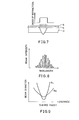
- FIGURE 8 shows an emission spectrum of the semiconductor laser of FIGURE 3 at the output of 3 mW.
- FIGURE 9 shows the beam waist position in the directions perpendicular to the PN junction and parallel with the PN junction.
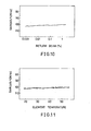
- FIGURE 10 shows the noise characteristic of the semiconductor laser of FIGURE 3 depending on the return beam reflected from the disc surface when the laser emission is conducted at 3 mW output.
- FIGURE 11 shows the relationship between the occurrence of the mode competition noise and the laser element temperature in the semiconductor laser of FIGURE 3. It will be clear from FIGURE 10 that the return beam noise is not generated because the laser emission is carried out in the multiple longitudinal mode. Further, the mode competition noise does not occur even at a high temperature as shown in FIGURE 11.
- the near-field pattern is stable because of the index guide structure formed near the both of the cleaved facets of the semiconductor laser.
- the astigmatism is less than 5 ⁇ m, and the semiconductor laser of the present invention ensures a good matching with an optical system.
- the present invention is not limited to the GaAs-GaAlAs semiconductor laser.
- the present invention is applicable to semiconductor lasers of different materials. Further, the present invention is not limited to the inner stripe type, but the present invention is applicable to semiconductor lasers of the planer type.
Landscapes
- Physics & Mathematics (AREA)
- Condensed Matter Physics & Semiconductors (AREA)
- General Physics & Mathematics (AREA)
- Electromagnetism (AREA)
- Optics & Photonics (AREA)
- Geometry (AREA)
- Semiconductor Lasers (AREA)
Applications Claiming Priority (2)
| Application Number | Priority Date | Filing Date | Title |
|---|---|---|---|
| JP59006922A JPS60150682A (ja) | 1984-01-17 | 1984-01-17 | 半導体レ−ザ素子 |
| JP6922/84 | 1984-01-17 |
Publications (3)
| Publication Number | Publication Date |
|---|---|
| EP0149563A2 true EP0149563A2 (de) | 1985-07-24 |
| EP0149563A3 EP0149563A3 (en) | 1986-08-27 |
| EP0149563B1 EP0149563B1 (de) | 1990-09-26 |
Family
ID=11651735
Family Applications (1)
| Application Number | Title | Priority Date | Filing Date |
|---|---|---|---|
| EP85300322A Expired EP0149563B1 (de) | 1984-01-17 | 1985-01-17 | Halbleiterlaser |
Country Status (4)
| Country | Link |
|---|---|
| US (1) | US4679200A (de) |
| EP (1) | EP0149563B1 (de) |
| JP (1) | JPS60150682A (de) |
| DE (1) | DE3579826D1 (de) |
Cited By (3)
| Publication number | Priority date | Publication date | Assignee | Title |
|---|---|---|---|---|
| EP0156365A3 (en) * | 1984-03-28 | 1987-06-03 | Kabushiki Kaisha Toshiba | Semiconductor laser |
| FR2606223A1 (fr) * | 1986-10-29 | 1988-05-06 | Seiko Epson Corp | Laser a semiconducteur et son procede de fabrication |
| US7469862B2 (en) | 2005-04-22 | 2008-12-30 | Goodrich Corporation | Aircraft engine nacelle inlet having access opening for electrical ice protection system |
Families Citing this family (11)
| Publication number | Priority date | Publication date | Assignee | Title |
|---|---|---|---|---|
| JPS60192380A (ja) * | 1984-03-13 | 1985-09-30 | Mitsubishi Electric Corp | 半導体レ−ザ装置 |
| JPS60201687A (ja) * | 1984-03-27 | 1985-10-12 | Sony Corp | 半導体レ−ザ− |
| JPS61289689A (ja) * | 1985-06-18 | 1986-12-19 | Mitsubishi Electric Corp | 半導体発光装置 |
| JPS621296A (ja) * | 1985-06-26 | 1987-01-07 | Sharp Corp | 多端子型半導体レ−ザ素子 |
| JPS6218783A (ja) * | 1985-07-17 | 1987-01-27 | Sharp Corp | 半導体レ−ザ素子 |
| JPS62130586A (ja) * | 1985-12-03 | 1987-06-12 | Matsushita Electric Ind Co Ltd | 半導体レ−ザ装置 |
| JPS62283685A (ja) * | 1986-05-31 | 1987-12-09 | Mitsubishi Electric Corp | 半導体レ−ザ装置の製造方法 |
| US4946802A (en) * | 1986-05-31 | 1990-08-07 | Mitsubishi Denki Kabushiki Kaisha | Semiconductor laser device fabricating method |
| JP2538258B2 (ja) * | 1987-06-20 | 1996-09-25 | 三洋電機株式会社 | 半導体レ―ザ |
| GB2318211B (en) * | 1996-10-09 | 1999-03-31 | Toshiba Cambridge Res Center | Optical waveguide structure |
| JP5261857B2 (ja) * | 2001-09-21 | 2013-08-14 | 日本電気株式会社 | 端面発光型半導体レーザおよび半導体レーザ・モジュール |
Family Cites Families (4)
| Publication number | Priority date | Publication date | Assignee | Title |
|---|---|---|---|---|
| US4280106A (en) * | 1979-05-15 | 1981-07-21 | Xerox Corporation | Striped substrate planar laser |
| JPS58197787A (ja) * | 1982-05-12 | 1983-11-17 | Nec Corp | 半導体レ−ザ |
| JPS5961982A (ja) * | 1982-09-30 | 1984-04-09 | Sony Corp | 半導体レ−ザ− |
| US4594718A (en) * | 1983-02-01 | 1986-06-10 | Xerox Corporation | Combination index/gain guided semiconductor lasers |
-
1984
- 1984-01-17 JP JP59006922A patent/JPS60150682A/ja active Pending
-
1985
- 1985-01-16 US US06/691,917 patent/US4679200A/en not_active Expired - Lifetime
- 1985-01-17 DE DE8585300322T patent/DE3579826D1/de not_active Expired - Lifetime
- 1985-01-17 EP EP85300322A patent/EP0149563B1/de not_active Expired
Cited By (3)
| Publication number | Priority date | Publication date | Assignee | Title |
|---|---|---|---|---|
| EP0156365A3 (en) * | 1984-03-28 | 1987-06-03 | Kabushiki Kaisha Toshiba | Semiconductor laser |
| FR2606223A1 (fr) * | 1986-10-29 | 1988-05-06 | Seiko Epson Corp | Laser a semiconducteur et son procede de fabrication |
| US7469862B2 (en) | 2005-04-22 | 2008-12-30 | Goodrich Corporation | Aircraft engine nacelle inlet having access opening for electrical ice protection system |
Also Published As
| Publication number | Publication date |
|---|---|
| US4679200A (en) | 1987-07-07 |
| DE3579826D1 (de) | 1990-10-31 |
| EP0149563A3 (en) | 1986-08-27 |
| JPS60150682A (ja) | 1985-08-08 |
| EP0149563B1 (de) | 1990-09-26 |
Similar Documents
| Publication | Publication Date | Title |
|---|---|---|
| US4594718A (en) | Combination index/gain guided semiconductor lasers | |
| EP0310038B1 (de) | Halbleiterlaser mit Oberflächenausstrahlung | |
| US4615032A (en) | Self-aligned rib-waveguide high power laser | |
| US4679200A (en) | Semiconductor laser | |
| EP0627799A1 (de) | Lichtmittierende Halbleitervorrichtung mit einer dritten Begrenzungsschicht | |
| US4803691A (en) | Lateral superradiance suppressing diode laser bar | |
| EP0162668A2 (de) | Halbleiterlaser | |
| EP0206818B1 (de) | Halbleiterlaservorrichtung | |
| EP0155151A2 (de) | Halbleiterlaser | |
| US4791649A (en) | Semiconductor laser device | |
| US5953358A (en) | Semiconductor laser device | |
| EP0302732B1 (de) | Halbleiterlaservorrichtung | |
| EP0145203A2 (de) | Halbleiterlaser | |
| Tada et al. | Uniform fabrication of highly reliable, 50–60 mW-class, 685 nm, window-mirror lasers for optical data storage | |
| US4377865A (en) | Semiconductor laser | |
| US4754462A (en) | Semiconductor laser device with a V-channel and a mesa | |
| EP0306314B1 (de) | Halbleiterlaser-Vorrichtung | |
| US4694461A (en) | Semiconductor laser array | |
| US4890292A (en) | Semiconductor laser device | |
| US4122410A (en) | Lateral mode control in semiconductor lasers | |
| US4951290A (en) | Semiconductor laser device | |
| US4530099A (en) | Planar narrow-stripe laser with improved charge carrier confinement | |
| US4847847A (en) | Semiconductor laser array | |
| US4745611A (en) | Buried twin ridge substrate laser | |
| KR100278626B1 (ko) | 반도체 레이저 다이오드 |
Legal Events
| Date | Code | Title | Description |
|---|---|---|---|
| PUAI | Public reference made under article 153(3) epc to a published international application that has entered the european phase |
Free format text: ORIGINAL CODE: 0009012 |
|
| AK | Designated contracting states |
Designated state(s): DE GB NL |
|
| PUAL | Search report despatched |
Free format text: ORIGINAL CODE: 0009013 |
|
| AK | Designated contracting states |
Kind code of ref document: A3 Designated state(s): DE GB NL |
|
| 17P | Request for examination filed |
Effective date: 19870225 |
|
| 17Q | First examination report despatched |
Effective date: 19890331 |
|
| GRAA | (expected) grant |
Free format text: ORIGINAL CODE: 0009210 |
|
| AK | Designated contracting states |
Kind code of ref document: B1 Designated state(s): DE GB NL |
|
| REF | Corresponds to: |
Ref document number: 3579826 Country of ref document: DE Date of ref document: 19901031 |
|
| PLBE | No opposition filed within time limit |
Free format text: ORIGINAL CODE: 0009261 |
|
| STAA | Information on the status of an ep patent application or granted ep patent |
Free format text: STATUS: NO OPPOSITION FILED WITHIN TIME LIMIT |
|
| 26N | No opposition filed | ||
| REG | Reference to a national code |
Ref country code: GB Ref legal event code: IF02 |
|
| PGFP | Annual fee paid to national office [announced via postgrant information from national office to epo] |
Ref country code: GB Payment date: 20040114 Year of fee payment: 20 |
|
| PGFP | Annual fee paid to national office [announced via postgrant information from national office to epo] |
Ref country code: NL Payment date: 20040121 Year of fee payment: 20 |
|
| PGFP | Annual fee paid to national office [announced via postgrant information from national office to epo] |
Ref country code: DE Payment date: 20040129 Year of fee payment: 20 |
|
| PG25 | Lapsed in a contracting state [announced via postgrant information from national office to epo] |
Ref country code: GB Free format text: LAPSE BECAUSE OF EXPIRATION OF PROTECTION Effective date: 20050116 |
|
| PG25 | Lapsed in a contracting state [announced via postgrant information from national office to epo] |
Ref country code: NL Free format text: LAPSE BECAUSE OF EXPIRATION OF PROTECTION Effective date: 20050117 |
|
| REG | Reference to a national code |
Ref country code: GB Ref legal event code: PE20 |
|
| NLV7 | Nl: ceased due to reaching the maximum lifetime of a patent |
Effective date: 20050117 |