EP0150522A2 - Datenverarbeitungssystem mit hierarchischem Speicherschutz - Google Patents
Datenverarbeitungssystem mit hierarchischem Speicherschutz Download PDFInfo
- Publication number
- EP0150522A2 EP0150522A2 EP84201482A EP84201482A EP0150522A2 EP 0150522 A2 EP0150522 A2 EP 0150522A2 EP 84201482 A EP84201482 A EP 84201482A EP 84201482 A EP84201482 A EP 84201482A EP 0150522 A2 EP0150522 A2 EP 0150522A2
- Authority
- EP
- European Patent Office
- Prior art keywords
- address
- segment
- bits
- data
- protection
- Prior art date
- Legal status (The legal status is an assumption and is not a legal conclusion. Google has not performed a legal analysis and makes no representation as to the accuracy of the status listed.)
- Granted
Links
Images























Classifications
-
- G—PHYSICS
- G06—COMPUTING OR CALCULATING; COUNTING
- G06F—ELECTRIC DIGITAL DATA PROCESSING
- G06F9/00—Arrangements for program control, e.g. control units
- G06F9/06—Arrangements for program control, e.g. control units using stored programs, i.e. using an internal store of processing equipment to receive or retain programs
- G06F9/30—Arrangements for executing machine instructions, e.g. instruction decode
- G06F9/30181—Instruction operation extension or modification
- G06F9/30196—Instruction operation extension or modification using decoder, e.g. decoder per instruction set, adaptable or programmable decoders
-
- G—PHYSICS
- G06—COMPUTING OR CALCULATING; COUNTING
- G06F—ELECTRIC DIGITAL DATA PROCESSING
- G06F12/00—Accessing, addressing or allocating within memory systems or architectures
- G06F12/02—Addressing or allocation; Relocation
- G06F12/08—Addressing or allocation; Relocation in hierarchically structured memory systems, e.g. virtual memory systems
- G06F12/10—Address translation
- G06F12/1009—Address translation using page tables, e.g. page table structures
-
- G—PHYSICS
- G06—COMPUTING OR CALCULATING; COUNTING
- G06F—ELECTRIC DIGITAL DATA PROCESSING
- G06F12/00—Accessing, addressing or allocating within memory systems or architectures
- G06F12/14—Protection against unauthorised use of memory or access to memory
- G06F12/1458—Protection against unauthorised use of memory or access to memory by checking the subject access rights
- G06F12/1491—Protection against unauthorised use of memory or access to memory by checking the subject access rights in a hierarchical protection system, e.g. privilege levels, memory rings
-
- G—PHYSICS
- G06—COMPUTING OR CALCULATING; COUNTING
- G06F—ELECTRIC DIGITAL DATA PROCESSING
- G06F9/00—Arrangements for program control, e.g. control units
- G06F9/06—Arrangements for program control, e.g. control units using stored programs, i.e. using an internal store of processing equipment to receive or retain programs
- G06F9/30—Arrangements for executing machine instructions, e.g. instruction decode
- G06F9/30181—Instruction operation extension or modification
-
- G—PHYSICS
- G06—COMPUTING OR CALCULATING; COUNTING
- G06F—ELECTRIC DIGITAL DATA PROCESSING
- G06F9/00—Arrangements for program control, e.g. control units
- G06F9/06—Arrangements for program control, e.g. control units using stored programs, i.e. using an internal store of processing equipment to receive or retain programs
- G06F9/30—Arrangements for executing machine instructions, e.g. instruction decode
- G06F9/30181—Instruction operation extension or modification
- G06F9/30189—Instruction operation extension or modification according to execution mode, e.g. mode flag
-
- G—PHYSICS
- G06—COMPUTING OR CALCULATING; COUNTING
- G06F—ELECTRIC DIGITAL DATA PROCESSING
- G06F11/00—Error detection; Error correction; Monitoring
- G06F11/07—Responding to the occurrence of a fault, e.g. fault tolerance
- G06F11/08—Error detection or correction by redundancy in data representation, e.g. by using checking codes
- G06F11/10—Adding special bits or symbols to the coded information, e.g. parity check, casting out 9's or 11's
- G06F11/1008—Adding special bits or symbols to the coded information, e.g. parity check, casting out 9's or 11's in individual solid state devices
- G06F11/1048—Adding special bits or symbols to the coded information, e.g. parity check, casting out 9's or 11's in individual solid state devices using arrangements adapted for a specific error detection or correction feature
- G06F11/106—Correcting systematically all correctable errors, i.e. scrubbing
Definitions
- a unique instruction In order to determine which instruction is to be decoded, a unique instruction must be used to set a "mode bit", i.e., a single bit which in one state indicates that the original instruction set is to be decoded and in the other state indicates that the extended instruction set is to be decoded.
- mode bit i.e., a single bit which in one state indicates that the original instruction set is to be decoded and in the other state indicates that the extended instruction set is to be decoded.
- the decoding subsystem In neither case can the decoding subsystem be made available to decode either of the both sets simultaneously.
- Such approach inserts a limitation on the overall machine operation since it is never possible to simultaneously decode instructions from different instruction sets of an overall super set thereof.
- the latter translation provides an accelerated address reference and can be accomplished by saving, at the end of every Long Address Translation, the address of the physical page which has been accessed.
- the physical page involved is stored in a high speed random access memory (RAL4) file designated in FIG. 7 at ATU translation store 100.
- RAL4 high speed random access memory
- a logical word address LA0-31 is received from the arithmetic logic unit (ALU) on the logical address bus 26 it is latched into a logical address register (LAR) 101 .
- the Index bits LA 15-21 are taken directly from the logical address bus to address four RAM stores, the first being a Tag store 102, which retains the tag portions of the logical addresses corresponding to the physical addresses saved in the ATU physical address (PA) translation store 100.
- the Index bits LA 15-21 are also supplied to a validity store RAM unit 103 and to a protection store RAM unit 104, as discussed below.
- the "tag" taken from the logical address register ( LAR 2-14 ) is written into the tag store 102 at the location selected by the index and the physical page address from the memory data register 106 (MD 18-31) is written into the translation store 100 at the location specified by the index.
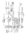
- the ATU configuration shown in FIG. 7 also contains further components which are used to place the translated physical address of a desired physical page table on the physical page address (PA) bus 27.
- PA physical page address
- HOPT high order page table
- LOPT low order page table
- the following diagrams depict the results of the control actions initiated by the arithmetic translation unit (ATU) to perform a long address translation in which a physical address is derived from a logical address by traversing the one-and two-level page tables in the main memory.
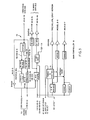
- Fi g 5 depicts a one-level page table traversal
- Fi g 6 idepicts a two-level page table traversal, the physical address bits 3-21 of the final physical address (i.e., the desired memory allocation data) being placed in the translation store 100 so that when the corresponding logical address is subsequently requires a translation, the physical address is available (an ATU HIT occurs) and there is no need for subsequent long address translation.
- the ATU begins with the physical address as shown at (2) of Fig 5. This address becomes bits 3-21 of the PTE address. Bits 13-21 of the logical word address become bits 22-30 of the PTE address. The ATU appends a zero to the right of the PTE address, making a 29-bit word address.
- the processor produces a physical address.
- the logical word address to be translated has the format shown in the diagram, the steps (1) to (4) being substantially the same as in
- Bits 3-21 of the PTE address specify the starting address of a page table. Bits 22-31 of the PTE address specify an offset from the start of the table to some PTE (labelled PTEn).
- the PT E specifies the starting address of a page table.
- the ATU now constructs the address of a second PTE from the address at (4).
- the physical address specified in bits 13-31 of the first (PTEn) becomes bits 3-21 of the address of the second PTEm.
- Bits 13-21 of the logical word address become bits 22-30 of the second PTE's address.
- the ATU appends a zero to the right of the second PTE address to make a 29-bit word address.
- Bits 3-21 of the second PTE address specify the starting address of a second page table. Bits 22-31 of the second PTE address specify an offset from the start of the second table to some PTE (labelled PTEm in Fig 6 ). The second PTE-specifies the starting address of a page, as shown at (5) in Fi g 6.
- the second PTEm's bits 13-31, the page address become bits 3-21 of the physical address and the page offset specified in bits 22-31 of the logical word address becomes bits 22-31 of the physical address, as shown at (6) in Fig 6. This last value is the final physical word address.
- the third and final source is to drive the physical page address bus 27 directly through a physical mode buffer 108, such buffer being used to address physical memory directly ( PHY 8-21 ) from buts LA 8-21 of the logical address bus.
- a physical mode buffer 108 such buffer being used to address physical memory directly ( PHY 8-21 ) from buts LA 8-21 of the logical address bus.
- Such buffer is enabled while the ATU unit is turned off (i.e., no address translation is required) since the physical address in that mode is the same as the logical address and no translation is necessary.
- the address bit sources for forming a low order or high order page table entry address in main memory in making a long address translation is formed from address fields in a segment base register (SBR) and from address fields in the logical address register.
- SBR segment base register
- the address fields of a segment base register can be depicted as follows:
- a validity storage protection check determines whether the corresponding block of memory to which a memory reference is made has been allocated and is accessible to the current user of the system.
- the validity storage field is a one-bit field which is located, for example, at bit zero of each of the segment base registers (located on an ATU board as discussed above) or at bit zero in each of the high order page table entry addresses and low order page table entry addresses.
- a "I" indicates that the corresponding block has been so allocated and is accessible whereas a "0" indicates that the user cannot use such a memory block.
- the execute protection field is a one-bit field which is located at a selected bit (e.g. bit 4) in each of the low order page table entry addresses and a check thereof determines whether instructions from a corresponding object page can or cannot be executed by the current user. If such an instruction fetch is not allowed, an execute error is signaled by the fault code bits on the CPD bus. Execute protection is normally checked only during the first fetch within a page and any additional instruction fetches are performed using the physical page address from the first fetch, which for such purpose is retained by the instruction processor.
- Ring maximization protection is utilized when the user is attempting to reference a logical location in memory in a lower ring-(segment) than the current ring of execution (CRE 1-3). Since such operation is not permitted by the system, the operation must be aborted if the user attempts to reference a lower ring than currently being used and a ring maximization error is signaled on the CPD bus. Since the logical address space is divided into eight rings, or segments, a ring which the user desires to reference can be indicated by bits 1-3, for example, of the logical address.
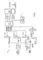
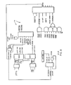
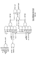
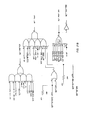
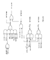
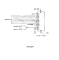
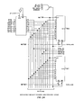
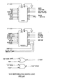
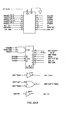
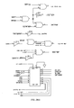
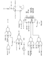
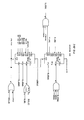
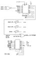
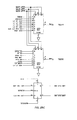
- FIGS. 8 and 9 The specific logic circuitry utilized for such protection checks (i.e., the protection store 104 and the protection logic 110 and the protection logic 111 associated therewith) is shown in FIGS. 8 and 9 .
- the protection store 104 and the protection logic 110 and the protection logic 111 associated therewith is shown in FIGS. 8 and 9 .
- loqic for the generation of the read error, write error, execution error and validity error signals is shown in FIG. 8 and logic for generating the defer error and ring maximization error signals being shown in FIG. 9.
- the read bracket of a data reference in any ring is the ring number. That is, a data address reference to segment 5 (ring 5) , for example, can never legitimately originate from an effective source which is greater than 5. In other words an effective source in segment 5 can never reference a ring lower than ring 5 and, therefore, if a reference from an effective source greater than 5 attempts to access ring 5 a ring maximum error (MAX ERR) will be signaled as shown by the logic in FIG. 7 .
- MAX ERR ring maximum error
- the ring maximization function is used to determine whether or not the reference is a valid ring reference and, if it is, the page table entry that references the address datum is examined to see if the page is a valid one. Then, if the read protection bit indicates that such valid page can be read, the read can be performed. If any one of the examinations shows a protection error (i.e., ring maximization error, validity error, or read error) the read is aborted and an appropriate fault code routine is called. Similarly, appropriate examination for protection errors for write access and execute access situations can also be performed.
- a protection error i.e., ring maximization error, validity error, or read error
- Any ring crossing attempts occur only as a result of an explicit attempt to do so by a program control instruction, and such explicit attempt can occur only if the following conditions are satisfied.
- the return address for outward returns is merely interpreted as a normal word address.
- the branch address is interpreted as follows: Bits 16-31 are interpreted as a "gate" into the specified segment (SBR of bits 1-3) in the target space. The gate number is used to verify that the specified gate is in the called segment and, upon verification, to associate on instruction address with the specified gate via a "gate array. in the called segment, as discussed below.
- the location of the gate array in any called segment is indicated by a pointer contained in particular locations of the called segment (e.g., in a particular embodiment the pointer locations may be specified as locations 34 and 35 in each segment.
- the structure of the gate array is as follows:
- the gate number of the pointer which referenced the target segment is compared with bits 16-31 of the first 32 bits of the gate array. If the gate number is greater than or equal to the maximum number of gates in the gate array, the ring crossing call is not permitted and a protection fault occurs (if the maximum number of gates is 0, the segment involved cannot be a valid target of an inward ring crossing call operation).
- the gate number is then used to index into one of the gates of the gate array which follows the first 32 bits thereof.
- the contents of the indexed gate are read and are used to control two actions.
- the effective source is compared to the gate bracket bits 1-3 of the indexed gate.
- the effective source must be less than or equal to the referenced gate bits and, if so, the P C offset bits 4-31 become the least significant 28 bits of the program counter and bits 1-3 of the program counter are set to the segment containing the gate array.
- the gate in a ring crossing operation is a permitted entry point to the ring to which the crossing is made, a new stack is constructed. In order to do so a stack switching operation must occur since there is only one stack per ring. Thus, before the new stack can be created, the contents of the current stack management registers must be saved at specified memory locations of the caller's ring.
- the callee's stack can then be created, the arguments from the caller's stack being copied onto the newly created callee's stack, the number of such arguments being specified by the X or the LC A LL instruction (see Appendix B). An appropriate check is first made to determine whether copying of all of the arguments would created a stack overflow condition. If so, a stack fault is signalled, the ring crossing being permitted and the fault being processed in the called ring.
- emulation control logic unit 115 In order to emulate operation of ECLIPSE address translation operations appropriate emulation control signals for placing the ATU in the ECLIPSE operating mode are required as shown by emulation control logic unit 115 which, in response to coded instructions generated by the microsequencer board 13 produces such signals to permit operation for 16-bit addresses equivalent to the memory management protection unit (MMPU) of ECLIPSE comparators as described in the aforesaid publications thereon.
- MMPU memory management protection unit
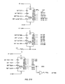
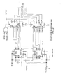
- FIGS. 10 to 28 Specific logic circuitry for implementing the various blocks of the address translation unit shown in FIGS.7 - 9 are shown in FIGS. 10 to 28.
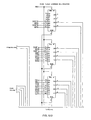
- FIG. 10 depicts the translation store unit 100 supplied with bits MD 18-31 from the memory data register 106 and in turn supplying the translated physical address bits 8-21 which have resulted from a translation of the logical address bits LA 15-21.
- FIG. 10 also shows the page table address multiplexer unit 107 and physical mode buffer unit 108. In addition, such figure includes the "last block" register unit 116 which during an ECLIPSE MMPU emulation operation provides the physical address bits PHY 8-21.
- FIG. 10 also shows the LMP Data Register.
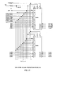
- FIG. 11 shows Tag Store 102 and Protection Store 104.
- Tag comparator unit 105 is depicted in FIG. 12.
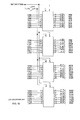
- Protection logic including fault detection and cache block crossing trap logic is depicted in FIGS.17 to 21 protection logic identification encoder unit 110 being shown in FIG. 17 the fault code bit drive unit 112 being shown in FIG.18 ring protection logic circuit 111 being shown in FIG.19 and the fault detection and cache block crossing logic being shown in FIGS. 20 and 21.
- Validity store unit 103 is shown in FIG. 22 together with translation purge logic and the multiplexer associated therewith.
- the translation register of FIG. 7 is depicted in detail in FIG. 23.
- the reference/modify storage and control logic unit is shown in FIG. 2 4, the state save drive unit associated therewith being depicted in FIG. 2 5.
- the 16 bit MMPU emulation control logic is shown in FIG. 26.
- ATU timing logic is shown in FIG.27 and suitable system code interface logic is shown in FIG. 28.
- SBR segment base registers
- the eight segment base registers of the system each contain a double word of a block of eight double words.
- the operation described here relates to the loading of such SBR's with an eight double-word block from memory, the starting address of which is contained in a selected accumulator of the system (e.g. AC0).
- the LSBRA operation then loads such block into the SBR's in the manner shown by the table designated in connection with the LSBRA instruction in Appendix B.
Landscapes
- Engineering & Computer Science (AREA)
- Theoretical Computer Science (AREA)
- Software Systems (AREA)
- Physics & Mathematics (AREA)
- General Engineering & Computer Science (AREA)
- General Physics & Mathematics (AREA)
- Computer Security & Cryptography (AREA)
- Storage Device Security (AREA)
- Memory System Of A Hierarchy Structure (AREA)
Applications Claiming Priority (4)
| Application Number | Priority Date | Filing Date | Title |
|---|---|---|---|
| US14368180A | 1980-04-25 | 1980-04-25 | |
| US143982 | 1980-04-25 | ||
| US06/143,982 US4434459A (en) | 1980-04-25 | 1980-04-25 | Data processing system having instruction responsive apparatus for both a basic and an extended instruction set |
| US143681 | 1980-04-25 |
Related Parent Applications (1)
| Application Number | Title | Priority Date | Filing Date |
|---|---|---|---|
| EP81301836A Division EP0039227A3 (en) | 1980-04-25 | 1981-04-27 | Data processing system |
Publications (3)
| Publication Number | Publication Date |
|---|---|
| EP0150522A2 true EP0150522A2 (de) | 1985-08-07 |
| EP0150522A3 EP0150522A3 (en) | 1986-12-30 |
| EP0150522B1 EP0150522B1 (de) | 1989-08-30 |
Family
ID=26841298
Family Applications (1)
| Application Number | Title | Priority Date | Filing Date |
|---|---|---|---|
| EP84201482A Expired EP0150522B1 (de) | 1980-04-25 | 1981-04-27 | Datenverarbeitungssystem mit hierarchischem Speicherschutz |
Country Status (1)
| Country | Link |
|---|---|
| EP (1) | EP0150522B1 (de) |
Cited By (4)
| Publication number | Priority date | Publication date | Assignee | Title |
|---|---|---|---|---|
| EP0230354A3 (en) * | 1986-01-16 | 1990-05-30 | International Business Machines Corporation | Enhanced handling of large virtual storage extents |
| EP0377431A3 (de) * | 1989-01-05 | 1992-01-22 | Bull HN Information Systems Inc. | Anordnung und Verfahren zur Übersetzung virtueller Adressen von nicht ausgerichteten Doppel-Wörtern |
| EP0458718A3 (en) * | 1990-05-24 | 1992-06-03 | International Business Machines Corporation | Method for controlling public access to a plurality of data objects within a data processing system |
| WO1993002419A1 (en) * | 1991-07-16 | 1993-02-04 | J.A.S. Technology (Australia) Pty. Ltd. | Protection system for computers |
Families Citing this family (1)
| Publication number | Priority date | Publication date | Assignee | Title |
|---|---|---|---|---|
| CN109165097B (zh) * | 2018-08-23 | 2021-06-08 | 北京九狐时代智能科技有限公司 | 一种数据处理方法以及数据处理装置 |
Family Cites Families (2)
| Publication number | Priority date | Publication date | Assignee | Title |
|---|---|---|---|---|
| FR2258112A5 (de) * | 1973-11-30 | 1975-08-08 | Honeywell Bull Soc Ind | |
| US3916385A (en) * | 1973-12-12 | 1975-10-28 | Honeywell Inf Systems | Ring checking hardware |
-
1981
- 1981-04-27 EP EP84201482A patent/EP0150522B1/de not_active Expired
Cited By (5)
| Publication number | Priority date | Publication date | Assignee | Title |
|---|---|---|---|---|
| EP0230354A3 (en) * | 1986-01-16 | 1990-05-30 | International Business Machines Corporation | Enhanced handling of large virtual storage extents |
| EP0377431A3 (de) * | 1989-01-05 | 1992-01-22 | Bull HN Information Systems Inc. | Anordnung und Verfahren zur Übersetzung virtueller Adressen von nicht ausgerichteten Doppel-Wörtern |
| EP0458718A3 (en) * | 1990-05-24 | 1992-06-03 | International Business Machines Corporation | Method for controlling public access to a plurality of data objects within a data processing system |
| US5414844A (en) * | 1990-05-24 | 1995-05-09 | International Business Machines Corporation | Method and system for controlling public access to a plurality of data objects within a data processing system |
| WO1993002419A1 (en) * | 1991-07-16 | 1993-02-04 | J.A.S. Technology (Australia) Pty. Ltd. | Protection system for computers |
Also Published As
| Publication number | Publication date |
|---|---|
| EP0150522A3 (en) | 1986-12-30 |
| EP0150522B1 (de) | 1989-08-30 |
Similar Documents
| Publication | Publication Date | Title |
|---|---|---|
| EP0150521A2 (de) | Datenverarbeitungssystem mit Unterbrechungsverarbeitung | |
| US4386399A (en) | Data processing system | |
| US4398243A (en) | Data processing system having a unique instruction processor system | |
| CA2024444C (en) | Process using virtual addressing in a non-privileged instruction to control the copying of a page of data in or between multiple media | |
| US5440710A (en) | Emulation of segment bounds checking using paging with sub-page validity | |
| JP3987577B2 (ja) | システム管理モード情報を他の情報と共にキャッシュに入れる方法および装置 | |
| EP0115179A2 (de) | Vorrichtung zur Übersetzung virtueller Speicheradressen mit kombiniert gemischter Adressierungstabelle und invertierter Seitentabelle | |
| JPH0198040A (ja) | メモリ管理システムおよびその動作方法 | |
| JPS58212694A (ja) | メモリシステム | |
| EP0321793B1 (de) | Gerät zur Zurückladeforcierung aus dem Hauptspeicher bei Cache-Speicherfehlern | |
| JPS6248258B2 (de) | ||
| US4392201A (en) | Diagnostic subsystem for a cache memory | |
| EP0039227A2 (de) | Datenverarbeitungsanlage | |
| US9639477B2 (en) | Memory corruption prevention system | |
| US7886205B2 (en) | Verification of a data processing system using overlapping address ranges | |
| EP0150522B1 (de) | Datenverarbeitungssystem mit hierarchischem Speicherschutz | |
| CN111527480B (zh) | 数据处理装置中的地址转换 | |
| EP0149858B1 (de) | Datenverarbeitungssystem | |
| EP0055579B1 (de) | Cache-Speicher mit Doppelwort-Zugriff | |
| EP0192578A2 (de) | Mehrbusanordnung mit einem Mikroprozessor mit getrennten Befehls- und Datenschnittstellen und Cachespeichern | |
| EP0272670A2 (de) | Segment-Deskriptor-Einheit | |
| EP0150523A2 (de) | Datenverarbeitungssystem mit Speichersystem | |
| US7386890B2 (en) | Method and apparatus to preserve a hash value of an executable module | |
| US20040064667A1 (en) | Method and system for providing a contiguous memory address space | |
| EP0389886B1 (de) | Logikeinrichtung zur Reduzierung von Ringen |
Legal Events
| Date | Code | Title | Description |
|---|---|---|---|
| PUAI | Public reference made under article 153(3) epc to a published international application that has entered the european phase |
Free format text: ORIGINAL CODE: 0009012 |
|
| AC | Divisional application: reference to earlier application |
Ref document number: 39227 Country of ref document: EP |
|
| AK | Designated contracting states |
Designated state(s): CH DE FR GB IT LI NL SE |
|
| PUAL | Search report despatched |
Free format text: ORIGINAL CODE: 0009013 |
|
| AK | Designated contracting states |
Kind code of ref document: A3 Designated state(s): CH DE FR GB IT LI NL SE |
|
| 17P | Request for examination filed |
Effective date: 19870527 |
|
| 17Q | First examination report despatched |
Effective date: 19880411 |
|
| GRAA | (expected) grant |
Free format text: ORIGINAL CODE: 0009210 |
|
| AC | Divisional application: reference to earlier application |
Ref document number: 39227 Country of ref document: EP |
|
| AK | Designated contracting states |
Kind code of ref document: B1 Designated state(s): CH DE FR GB IT LI NL SE |
|
| PG25 | Lapsed in a contracting state [announced via postgrant information from national office to epo] |
Ref country code: SE Effective date: 19890830 Ref country code: LI Effective date: 19890830 Ref country code: IT Free format text: LAPSE BECAUSE OF FAILURE TO SUBMIT A TRANSLATION OF THE DESCRIPTION OR TO PAY THE FEE WITHIN THE PRESCRIBED TIME-LIMIT;WARNING: LAPSES OF ITALIAN PATENTS WITH EFFECTIVE DATE BEFORE 2007 MAY HAVE OCCURRED AT ANY TIME BEFORE 2007. THE CORRECT EFFECTIVE DATE MAY BE DIFFERENT FROM THE ONE RECORDED. Effective date: 19890830 Ref country code: CH Effective date: 19890830 |
|
| REF | Corresponds to: |
Ref document number: 3177097 Country of ref document: DE Date of ref document: 19891005 |
|
| ET | Fr: translation filed | ||
| REG | Reference to a national code |
Ref country code: CH Ref legal event code: PL |
|
| PLBE | No opposition filed within time limit |
Free format text: ORIGINAL CODE: 0009261 |
|
| STAA | Information on the status of an ep patent application or granted ep patent |
Free format text: STATUS: NO OPPOSITION FILED WITHIN TIME LIMIT |
|
| 26N | No opposition filed | ||
| PGFP | Annual fee paid to national office [announced via postgrant information from national office to epo] |
Ref country code: NL Payment date: 19930430 Year of fee payment: 13 |
|
| PG25 | Lapsed in a contracting state [announced via postgrant information from national office to epo] |
Ref country code: NL Effective date: 19941101 |
|
| NLV4 | Nl: lapsed or anulled due to non-payment of the annual fee | ||
| PGFP | Annual fee paid to national office [announced via postgrant information from national office to epo] |
Ref country code: DE Payment date: 19980323 Year of fee payment: 18 |
|
| PGFP | Annual fee paid to national office [announced via postgrant information from national office to epo] |
Ref country code: FR Payment date: 19990317 Year of fee payment: 19 |
|
| PGFP | Annual fee paid to national office [announced via postgrant information from national office to epo] |
Ref country code: GB Payment date: 19990322 Year of fee payment: 19 |
|
| PG25 | Lapsed in a contracting state [announced via postgrant information from national office to epo] |
Ref country code: DE Free format text: LAPSE BECAUSE OF NON-PAYMENT OF DUE FEES Effective date: 20000201 |
|
| PG25 | Lapsed in a contracting state [announced via postgrant information from national office to epo] |
Ref country code: GB Free format text: LAPSE BECAUSE OF NON-PAYMENT OF DUE FEES Effective date: 20000427 |
|
| GBPC | Gb: european patent ceased through non-payment of renewal fee |
Effective date: 20000427 |
|
| PG25 | Lapsed in a contracting state [announced via postgrant information from national office to epo] |
Ref country code: FR Free format text: LAPSE BECAUSE OF NON-PAYMENT OF DUE FEES Effective date: 20001229 |
|
| REG | Reference to a national code |
Ref country code: FR Ref legal event code: ST |