EP0150929A2 - Substrat mit optischen Verbindungssystemen zwischen den auf dem Substrat montierten Bausteinen - Google Patents
Substrat mit optischen Verbindungssystemen zwischen den auf dem Substrat montierten Bausteinen Download PDFInfo
- Publication number
- EP0150929A2 EP0150929A2 EP85300154A EP85300154A EP0150929A2 EP 0150929 A2 EP0150929 A2 EP 0150929A2 EP 85300154 A EP85300154 A EP 85300154A EP 85300154 A EP85300154 A EP 85300154A EP 0150929 A2 EP0150929 A2 EP 0150929A2
- Authority
- EP
- European Patent Office
- Prior art keywords
- board
- communication system
- optical communication
- silicon
- support
- Prior art date
- Legal status (The legal status is an assumption and is not a legal conclusion. Google has not performed a legal analysis and makes no representation as to the accuracy of the status listed.)
- Withdrawn
Links
Images


Classifications
-
- H—ELECTRICITY
- H10—SEMICONDUCTOR DEVICES; ELECTRIC SOLID-STATE DEVICES NOT OTHERWISE PROVIDED FOR
- H10F—INORGANIC SEMICONDUCTOR DEVICES SENSITIVE TO INFRARED RADIATION, LIGHT, ELECTROMAGNETIC RADIATION OF SHORTER WAVELENGTH OR CORPUSCULAR RADIATION
- H10F55/00—Radiation-sensitive semiconductor devices covered by groups H10F10/00, H10F19/00 or H10F30/00 being structurally associated with electric light sources and electrically or optically coupled thereto
-
- G—PHYSICS
- G02—OPTICS
- G02B—OPTICAL ELEMENTS, SYSTEMS OR APPARATUS
- G02B6/00—Light guides; Structural details of arrangements comprising light guides and other optical elements, e.g. couplings
- G02B6/24—Coupling light guides
- G02B6/42—Coupling light guides with opto-electronic elements
- G02B6/43—Arrangements comprising a plurality of opto-electronic elements and associated optical interconnections
-
- H—ELECTRICITY
- H04—ELECTRIC COMMUNICATION TECHNIQUE
- H04B—TRANSMISSION
- H04B10/00—Transmission systems employing electromagnetic waves other than radio-waves, e.g. infrared, visible or ultraviolet light, or employing corpuscular radiation, e.g. quantum communication
- H04B10/80—Optical aspects relating to the use of optical transmission for specific applications, not provided for in groups H04B10/03 - H04B10/70, e.g. optical power feeding or optical transmission through water
- H04B10/801—Optical aspects relating to the use of optical transmission for specific applications, not provided for in groups H04B10/03 - H04B10/70, e.g. optical power feeding or optical transmission through water using optical interconnects, e.g. light coupled isolators, circuit board interconnections
Definitions
- This invention relates to a system for communication between semiconductor chips on a semiconductor substrate.
- Prior art complex semiconductor circuits have often been constructed by use of plastic or ceramic circuit board having semiconductor packages mounted thereon with interconnection or communication between semiconductor packages taking place via conductors formed on the circuit board. Problems of heat dissipation and cross talk are minimized in such circuits by spreading out the components sufficiently on the circuit board surface. It is also known in the prior art that, as the signal being communicated increases to a clock rate of over about 50 megahertz, the conductors on the printed circuit board begin to act as transmission lines and display capacitive and inductive properties. It is therefore necessary that appropriate measures be taken as in the case of transmission lines to obtain proper impedance matching to avoid reflections and the like. This problem is relatively minor and, in general, no particular attention was needed in the past if the check rate was below about 10 megahertz.
- a complex circuit composed of a circuit board which is formed of elemental silicon in the form of a slice and circuit components in the form of semiconductor integrated circuits thereon which are preferably formed of a Group III-V compound.
- Signals from each of the integrated circuits are transmitted to other integrated circuits on the board or externally of the board either by conventional printed conductors on the board or, preferably, by means of a laser formed in each integrated circuit at each output terminal thereon which transmits light signals along light conducting members in the silicon board to photo responsive elements at the input locations on other ones of the integrated circuits on the board for external to the board.
- each light emitting output will be composed preferably of a laser diode or the like and each input member will be composed preferably of a photo responsive diode or the like.
- the light signal is transferred from an integrated circuit output to an integrated circuit input or to a device external to the board by means of light conducting members.
- These light conducting members may be light conducting rods positioned either on the surface of the board or in grooves formed therein.
- the light conducting members can be silicon dioxide paths formed in the silicon circuit board by selective oxidation of the silicon board to form silicon dioxide light conducting paths therein. Each light conducting path will be coupled between a light emitting output from an integrated circuit and a light emitting input of another integrated circuit or travel to the edge of the circuit board for transmission external of the board.
- the light conducting member will be coupled to the light emitting member and the light receiving member of the integrated circuits by standard coupling means such as a light conducting epoxy or the like as are well known in the art.
- standard coupling means such as a light conducting epoxy or the like as are well known in the art.
- Such coupling techniques are shown in "Photo-Coupled Logic - A Hopeful Prospect", by D. A. Fraser (get the rest of this article data), pages 31 to 34; "Coupling Light Sources to Fibers" by Mark L. Dakss, Laser Focus, December, 1975, pages 31 to 34; Optical Waveguides Fabricated by Preferential Etching” by Won-Tien Tsang, Cheng-Chung Tseng, and Shyh Wang, Applied Optics, Vol. 14, No.
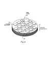
- a circuit board 1 formed of a silicon slice and having positioned thereon a plurality of semiconductor chips 3 preferably formed from a Group III-V material, which are secured to the top surface of the board 1 by appropriate bonding techniques.
- a plurality of fiber optic channels 5 are formed in or on the board in a manner to be described in more detail hereinbelow.
- Coupling elements 7 couple outputs 9 (Fig. 3) from the chip 3 to optic fiber channels 5 and also couple the optic fiber channels 5 to inputs 11 (Fig. 3) to the chips 3.
- Each of the chips 3 has either or both of a light emitting output element 9 which can be in the form of a laser diode which is coupled to one of the optic fiber channels 5 as shown in Fig. 3 and an input element 11, preferably in the form of a photo responsive diode which is also coupled to an optic fiber channel 5.
- the optical fiber channels 5 as shown in Figure 3 also provide communication between plural circuit boards or a circuit board and an external optical transmitter and/or receiver.
- the fiber optic channel 5 can be formed in several ways. In accordance with the first embodiment, grooves are formed in the upper surface of the circuit board 1 and standard fiber optic elements 5 are deposited and secured therein. When such standard fiber optic elements are utilized, the material from which the circuit board is formed need not be silicon but can be any standard board material.
- the circuit board 1 will be of crystalline silicon and the optic fiber channels 5 are formed therein bv standard semiconductor oxidation techniques wherein, for example, a silicon nitride pattern will be formed on the surface of the board 1 and the board will then either be etched in the regions where the optic fiber channels are to be formed with subsequent oxidation of the exposed silicon to fill the channel with silicon dioxide or, alternatively, after pattern formation with silicon nitride, the exposed silicon will be oxidized with subsequent optional etching back of the silicon oxide formed to an appropriate level if desired or required.
- the silicon dioxide formed by oxidation of the silicon board will act as an optic fiber channel and will have light conducting properties as is shown in the above mentioned publications.
- the semiconductor chips 3 will preferably be formed from a Group III-V compound, preferably gallium arsenide, so that, in addition to circuit components, either one or more laser diodes 9 or light responsive devices 11 or both can be formed in each of the chips to permit communication both into and out of each chip to provide the I/O terminals therefore. It should be understood that each chip can have a plurality of optical output devices 9 and/or a plurality of optical input devices 11.
- each of the optical fiber channels or conductors 5 is a transmitter of light, and since light signals can go up to about 2GHz bandwidth, it is possible to replace, for example, 10 electrical signals by one light conductor 5, each with a 200 MHz signal bandwidth. It is therefore apparent that, since plural different signals can be placed on the same line, an equivalent number of input and/or output terminals can be eliminated physically from the chip itself, thereby materially decreasing the space requirement.
- optical signals since optical signals are being utilized, there is no problem of impedance matching or other problems resulting from the use of high frequencies.
- the light is confined to the optical fiber or guide, there will be no cross talk across channels. Also, the problem of heat generation is substantially minimized by the use of optical transmissions.
- FIG 4 there is shown a further embodiment of the invention.
- a silicon circuit board 21 having mesas 23 formed in selected regions on the surface thereof which line up with alignment holes 25 formed on the surface of a gallium arsenide chip 27 of the type known in the art as a "flipchip".
- the mesas 23 are formed by standard well known orientation dependent etchants (ODE) to provide the desired mesa shape.
- the chip 27 includes a laser diode 29 which is lined up with an optical link 31 on the surface of the board 21 due to the selective formation of the mesas 23 to provide the alinement.
- the optical link 31 can be an optical fiber placed in a groove formed in the board 21 or on the surface of the board 21 or can be an S i 02 path formed in the board in the manner described hereinabove and in the above noted publications. Also shown is a further chip 33 positioned over mesas 35 which are the same as mesas 23 having a phototransistor 37 lined up with the optical link 31. Information at optical frequencies is transmitted from laser 29 to phototransistor 37 via optical link 31.
- the ODE mesas 23 are coupled to pads on the chips 27 and 33 to provide a voltage source, ground connection and as a signal input and output as well as for alignment as noted above.
- Boards of the type shown in Figures 1 to 4 can be stacked as shown in Figure 5. Communication among the stacked boards can be by electrical connection in standard manner and/or by running optical links from board to board. As shown in Figure 5, four boards 51 are stacked, one atop the other. Gallium arsenide chips 53 are positioned on the boards and interconnected on each board 51 by optical links 55. Optical fibers (not shown) travel between optical links 51 from any board 51 to and optical link on a further board 51 to provide optical communication between boards.
- the board itself is preferably a silicon substrate, wherein the optical fibers are formed in the board itself by standard integrated circuit processing techniques and wherein Group III-V semiconductor devices are utilized for transmitting and receiving the optical signals transmitted via the circuit board itself.
Landscapes
- Physics & Mathematics (AREA)
- Electromagnetism (AREA)
- Engineering & Computer Science (AREA)
- Computer Networks & Wireless Communication (AREA)
- Signal Processing (AREA)
- General Physics & Mathematics (AREA)
- Optics & Photonics (AREA)
- Optical Communication System (AREA)
- Solid State Image Pick-Up Elements (AREA)
- Semiconductor Lasers (AREA)
- Optical Couplings Of Light Guides (AREA)
Applications Claiming Priority (2)
| Application Number | Priority Date | Filing Date | Title |
|---|---|---|---|
| US06/571,044 US5009476A (en) | 1984-01-16 | 1984-01-16 | Semiconductor layer with optical communication between chips disposed therein |
| US571044 | 1984-01-16 |
Publications (2)
| Publication Number | Publication Date |
|---|---|
| EP0150929A2 true EP0150929A2 (de) | 1985-08-07 |
| EP0150929A3 EP0150929A3 (de) | 1988-06-22 |
Family
ID=24282099
Family Applications (1)
| Application Number | Title | Priority Date | Filing Date |
|---|---|---|---|
| EP85300154A Withdrawn EP0150929A3 (de) | 1984-01-16 | 1985-01-10 | Substrat mit optischen Verbindungssystemen zwischen den auf dem Substrat montierten Bausteinen |
Country Status (3)
| Country | Link |
|---|---|
| US (1) | US5009476A (de) |
| EP (1) | EP0150929A3 (de) |
| JP (1) | JPH071792B2 (de) |
Cited By (13)
| Publication number | Priority date | Publication date | Assignee | Title |
|---|---|---|---|---|
| EP0247722A1 (de) * | 1986-05-19 | 1987-12-02 | BRITISH TELECOMMUNICATIONS public limited company | Homodyne Verbindungen von integrierten Schaltungen |
| DE3720153A1 (de) * | 1987-06-16 | 1988-12-29 | Siemens Ag | Anordnung zur optoelektronischen kopplung von integrierten schaltungen, die in mindestens zwei halbleiterscheiben enthalten sind |
| US4851695A (en) * | 1986-09-30 | 1989-07-25 | Siemens Aktiengesellschaft | Optoelectronic coupling element with transparent spacer elements |
| US4857746A (en) * | 1986-09-30 | 1989-08-15 | Siemens Aktiengesellschaft | Method for producing an optocoupler |
| US4888625A (en) * | 1986-09-30 | 1989-12-19 | Siemens Aktiengesellschaft | Optoelectronic coupling element, and method of making same |
| EP0322218A3 (en) * | 1987-12-21 | 1990-03-28 | Physical Optics Corporation | Holographic planar optical interconnect |
| WO1990004835A1 (de) * | 1988-10-19 | 1990-05-03 | Wendt Hans J | Digitalrechner mit einer multiprozessor-anordnung |
| EP0331338A3 (de) * | 1988-03-03 | 1991-01-16 | AT&T Corp. | Untereinheiten für hybrid-integrierte optoelektronische Schaltkreise |
| EP0331331A3 (de) * | 1988-03-03 | 1991-01-16 | AT&T Corp. | Untereinheit für optoelektronische Bauelemente |
| EP0532469A1 (de) * | 1991-09-10 | 1993-03-17 | Centre Suisse D'electronique Et De Microtechnique S.A. | Verfahren zur Positionierung eines ersten Substrats auf ein zweites und so hergestellte mikromechanische Positioniervorrichtung |
| WO1993015424A1 (en) * | 1992-01-28 | 1993-08-05 | British Telecommunications Public Limited Company | Alignment of integrated optical components |
| EP0599212A1 (de) * | 1992-11-25 | 1994-06-01 | Robert Bosch Gmbh | Anordnung zur Ankopplung eines Lichtwellenleiters an ein lichtaussendendes oder -empfangendes Element |
| WO2002014915A3 (en) * | 2000-08-17 | 2003-05-01 | Univ Mcmaster | Silicon-on-insulator optical waveguide fabrication by local oxidation of silicon |
Families Citing this family (34)
| Publication number | Priority date | Publication date | Assignee | Title |
|---|---|---|---|---|
| US5159700A (en) * | 1984-01-16 | 1992-10-27 | Texas Instruments Incorporated | Substrate with optical communication systems between chips mounted thereon and monolithic integration of optical I/O on silicon substrates |
| JPH0642527B2 (ja) * | 1989-10-10 | 1994-06-01 | 日本電気株式会社 | 光導波路を用いた情報処理装置 |
| US5059475A (en) * | 1990-06-29 | 1991-10-22 | Photonic Integration Research, Inc. | Apparatus and method of forming optical waveguides on metalized substrates |
| US5834841A (en) * | 1990-09-28 | 1998-11-10 | Kabushiki Kaisha Toshiba | Semiconductor device enabling temperature control in the chip thereof |
| US5119451A (en) * | 1990-12-31 | 1992-06-02 | Texas Instruments Incorporated | Optical waveguides as interconnects from integrated circuit to integrated circuit and packaging method using same |
| EP0536829B1 (de) * | 1991-10-08 | 1997-02-05 | Koninklijke Philips Electronics N.V. | Optoelektronische Halbleiteranordnung mit einem Strahlungsleiter und Verfahren zum Herstellen einer derartigen Anordnung |
| US5208879A (en) * | 1991-10-18 | 1993-05-04 | International Business Machines Corporation | Optical signal distribution system |
| EP0548440A1 (de) * | 1991-12-23 | 1993-06-30 | International Business Machines Corporation | Zweiteilige Zusammensetzung für optoelektronische Integration |
| US5199087A (en) * | 1991-12-31 | 1993-03-30 | Texas Instruments Incorporated | Optoelectronic integrated circuit for transmitting optical and electrical signals and method of forming same |
| US5268973A (en) * | 1992-01-21 | 1993-12-07 | The University Of Texas System | Wafer-scale optical bus |
| US5259051A (en) * | 1992-08-28 | 1993-11-02 | At&T Bell Laboratories | Optical fiber interconnection apparatus and methods of making interconnections |
| JPH0786555A (ja) * | 1993-09-16 | 1995-03-31 | Hitachi Ltd | 3次元光・電子集積回路 |
| US5818984A (en) * | 1996-11-18 | 1998-10-06 | International Business Machines Corporation | Optoelectronic interconnection of integrated circuits |
| US5812708A (en) * | 1996-12-31 | 1998-09-22 | Intel Corporation | Method and apparatus for distributing an optical clock in an integrated circuit |
| US6453377B1 (en) | 1998-06-16 | 2002-09-17 | Micron Technology, Inc. | Computer including optical interconnect, memory unit, and method of assembling a computer |
| US6125217A (en) * | 1998-06-26 | 2000-09-26 | Intel Corporation | Clock distribution network |
| US6690845B1 (en) | 1998-10-09 | 2004-02-10 | Fujitsu Limited | Three-dimensional opto-electronic modules with electrical and optical interconnections and methods for making |
| US6706546B2 (en) | 1998-10-09 | 2004-03-16 | Fujitsu Limited | Optical reflective structures and method for making |
| US6343171B1 (en) | 1998-10-09 | 2002-01-29 | Fujitsu Limited | Systems based on opto-electronic substrates with electrical and optical interconnections and methods for making |
| US6611635B1 (en) | 1998-10-09 | 2003-08-26 | Fujitsu Limited | Opto-electronic substrates with electrical and optical interconnections and methods for making |
| US6684007B2 (en) | 1998-10-09 | 2004-01-27 | Fujitsu Limited | Optical coupling structures and the fabrication processes |
| US6845184B1 (en) | 1998-10-09 | 2005-01-18 | Fujitsu Limited | Multi-layer opto-electronic substrates with electrical and optical interconnections and methods for making |
| US6785447B2 (en) | 1998-10-09 | 2004-08-31 | Fujitsu Limited | Single and multilayer waveguides and fabrication process |
| US6252999B1 (en) * | 1998-12-23 | 2001-06-26 | Aurora Systems, Inc. | Planar reflective light valve backplane |
| JP2001148485A (ja) * | 1999-09-06 | 2001-05-29 | Seiko Epson Corp | 半導体装置 |
| AU2119301A (en) | 1999-10-22 | 2001-05-08 | Teraconnect, Inc. | Wafer scale integration and remoted subsystems using opto-electronic transceivers |
| JP2001274528A (ja) | 2000-01-21 | 2001-10-05 | Fujitsu Ltd | 薄膜デバイスの基板間転写方法 |
| US6752539B2 (en) * | 2002-06-28 | 2004-06-22 | International Buisness Machines Corporation | Apparatus and system for providing optical bus interprocessor interconnection |
| US20050031291A1 (en) * | 2003-03-24 | 2005-02-10 | Renfeng Gao | Assembly of device components and sub-systems |
| US7369718B2 (en) * | 2004-01-23 | 2008-05-06 | Intel Corporation | Package substrate pattern to accommodate optical waveguide |
| US7570849B2 (en) * | 2005-06-21 | 2009-08-04 | Hewlett-Packard Development Company, L.P. | Integrated circuit device having optically coupled layers |
| USD617289S1 (en) * | 2007-03-29 | 2010-06-08 | Luminus Devices, Inc. | LED package |
| WO2013086047A1 (en) | 2011-12-06 | 2013-06-13 | Cornell University | Integrated multi-chip module optical interconnect platform |
| US8548288B2 (en) * | 2011-12-20 | 2013-10-01 | Oracle International Corporation | Efficient inter-chip optical coupling |
Family Cites Families (20)
| Publication number | Priority date | Publication date | Assignee | Title |
|---|---|---|---|---|
| US2982883A (en) * | 1957-08-23 | 1961-05-02 | Hughes Aircraft Co | Electrical component locking arrangement |
| US3535532A (en) * | 1964-06-29 | 1970-10-20 | Texas Instruments Inc | Integrated circuit including light source,photodiode and associated components |
| CA874623A (en) * | 1966-09-28 | 1971-06-29 | A. Schuster Marvin | Radiation sensitive switching system for an array of elements |
| JPS4846278A (de) * | 1971-10-06 | 1973-07-02 | ||
| JPS5544429B2 (de) * | 1973-05-11 | 1980-11-12 | ||
| JPS5037993A (de) * | 1973-08-09 | 1975-04-09 | ||
| US3879606A (en) * | 1973-09-24 | 1975-04-22 | Texas Instruments Inc | Light projection coupling of semiconductor type devices through the use of thermally grown or deposited SiO{HD 2 {B films |
| US3956673A (en) * | 1974-02-14 | 1976-05-11 | Lockheed Aircraft Corporation | Printed circuit modules cooled by rack with forced air |
| GB1458544A (en) | 1974-03-21 | 1976-12-15 | Standard Telephones Cables Ltd | Semiconductor laser stacks |
| US4011575A (en) * | 1974-07-26 | 1977-03-08 | Litton Systems, Inc. | Light emitting diode array having a plurality of conductive paths for each light emitting diode |
| US4149088A (en) * | 1975-03-06 | 1979-04-10 | Lemelson Jerome H | Electro-optical circuits and manufacturing |
| US4169001A (en) * | 1976-10-18 | 1979-09-25 | International Business Machines Corporation | Method of making multilayer module having optical channels therein |
| JPS5946434B2 (ja) * | 1978-01-10 | 1984-11-12 | キヤノン株式会社 | 半導体レ−ザ装置 |
| US4274104A (en) * | 1979-05-21 | 1981-06-16 | International Business Machines Corporation | Electrooptical integrated circuit communication |
| JPS5651884A (en) * | 1979-10-03 | 1981-05-09 | Hitachi Ltd | Light sending and recieving element |
| JPS5678180A (en) * | 1979-11-30 | 1981-06-26 | Hitachi Ltd | Light receiving device |
| US4360246A (en) * | 1980-05-23 | 1982-11-23 | Hughes Aircraft Company | Integrated waveguide and FET detector |
| US4355321A (en) * | 1981-02-02 | 1982-10-19 | Varian Associates, Inc. | Optoelectronic assembly including light transmissive single crystal semiconductor window |
| US4533833A (en) * | 1982-08-19 | 1985-08-06 | At&T Bell Laboratories | Optically coupled integrated circuit array |
| US4535251A (en) * | 1982-12-21 | 1985-08-13 | International Rectifier Corporation | A.C. Solid state relay circuit and structure |
-
1984
- 1984-01-16 US US06/571,044 patent/US5009476A/en not_active Expired - Lifetime
-
1985
- 1985-01-10 EP EP85300154A patent/EP0150929A3/de not_active Withdrawn
- 1985-01-14 JP JP60004841A patent/JPH071792B2/ja not_active Expired - Lifetime
Cited By (16)
| Publication number | Priority date | Publication date | Assignee | Title |
|---|---|---|---|---|
| EP0247722A1 (de) * | 1986-05-19 | 1987-12-02 | BRITISH TELECOMMUNICATIONS public limited company | Homodyne Verbindungen von integrierten Schaltungen |
| US4844571A (en) * | 1986-05-19 | 1989-07-04 | Stanley Ian W | Homodyne interconnections of integrated circuits |
| US4851695A (en) * | 1986-09-30 | 1989-07-25 | Siemens Aktiengesellschaft | Optoelectronic coupling element with transparent spacer elements |
| US4857746A (en) * | 1986-09-30 | 1989-08-15 | Siemens Aktiengesellschaft | Method for producing an optocoupler |
| US4888625A (en) * | 1986-09-30 | 1989-12-19 | Siemens Aktiengesellschaft | Optoelectronic coupling element, and method of making same |
| DE3720153A1 (de) * | 1987-06-16 | 1988-12-29 | Siemens Ag | Anordnung zur optoelektronischen kopplung von integrierten schaltungen, die in mindestens zwei halbleiterscheiben enthalten sind |
| EP0322218A3 (en) * | 1987-12-21 | 1990-03-28 | Physical Optics Corporation | Holographic planar optical interconnect |
| EP0331338A3 (de) * | 1988-03-03 | 1991-01-16 | AT&T Corp. | Untereinheiten für hybrid-integrierte optoelektronische Schaltkreise |
| EP0331331A3 (de) * | 1988-03-03 | 1991-01-16 | AT&T Corp. | Untereinheit für optoelektronische Bauelemente |
| WO1990004835A1 (de) * | 1988-10-19 | 1990-05-03 | Wendt Hans J | Digitalrechner mit einer multiprozessor-anordnung |
| EP0532469A1 (de) * | 1991-09-10 | 1993-03-17 | Centre Suisse D'electronique Et De Microtechnique S.A. | Verfahren zur Positionierung eines ersten Substrats auf ein zweites und so hergestellte mikromechanische Positioniervorrichtung |
| CH685522A5 (fr) * | 1991-09-10 | 1995-07-31 | Suisse Electronique Microtech | Procédé pour positionner un premier substrat sur un second substrat et dispositif micromécanique de positionnement obtenu. |
| WO1993015424A1 (en) * | 1992-01-28 | 1993-08-05 | British Telecommunications Public Limited Company | Alignment of integrated optical components |
| US5656507A (en) * | 1992-01-28 | 1997-08-12 | British Telecommunications Public Limited Company | Process for self-aligning circuit components brought into abutment by surface tension of a molten material and bonding under tension |
| EP0599212A1 (de) * | 1992-11-25 | 1994-06-01 | Robert Bosch Gmbh | Anordnung zur Ankopplung eines Lichtwellenleiters an ein lichtaussendendes oder -empfangendes Element |
| WO2002014915A3 (en) * | 2000-08-17 | 2003-05-01 | Univ Mcmaster | Silicon-on-insulator optical waveguide fabrication by local oxidation of silicon |
Also Published As
| Publication number | Publication date |
|---|---|
| JPS60169167A (ja) | 1985-09-02 |
| EP0150929A3 (de) | 1988-06-22 |
| US5009476A (en) | 1991-04-23 |
| JPH071792B2 (ja) | 1995-01-11 |
Similar Documents
| Publication | Publication Date | Title |
|---|---|---|
| US5009476A (en) | Semiconductor layer with optical communication between chips disposed therein | |
| US5159700A (en) | Substrate with optical communication systems between chips mounted thereon and monolithic integration of optical I/O on silicon substrates | |
| US10962728B2 (en) | Co-packaged optics and transceiver | |
| US6611635B1 (en) | Opto-electronic substrates with electrical and optical interconnections and methods for making | |
| US6706546B2 (en) | Optical reflective structures and method for making | |
| US6343171B1 (en) | Systems based on opto-electronic substrates with electrical and optical interconnections and methods for making | |
| US6684007B2 (en) | Optical coupling structures and the fabrication processes | |
| JP3366074B2 (ja) | 光送受信機モジュールおよびその製造方法 | |
| EP0511931B1 (de) | Vorrichtung für ein faseroptisches Interface | |
| US6845184B1 (en) | Multi-layer opto-electronic substrates with electrical and optical interconnections and methods for making | |
| US20240241329A1 (en) | Heterogeneous packaging integration of photonic and electronic elements | |
| US5241614A (en) | Apparatus and a method for an optical fiber interface | |
| US5416872A (en) | Arrangement for interconnecting an optical fiber an optoelectronic component | |
| US7141778B2 (en) | Semiconductor device, optoelectronic board, and production methods therefor | |
| JP3728147B2 (ja) | 光電気混載配線基板 | |
| US20060177173A1 (en) | Vertical stacking of multiple integrated circuits including SOI-based optical components | |
| US7667311B2 (en) | LSI package provided with interface module, and transmission line header employed in the package | |
| US10466413B2 (en) | Opto-electronic system including optical input/output device | |
| US6862378B2 (en) | Silicon-based high speed optical wiring board | |
| EP0478750B1 (de) | Optisches Signalverteilungsnetzwerk | |
| JP3684112B2 (ja) | 光電気混載配線基板、その駆動方法、およびそれを用いた電子回路装置 | |
| JPH06132516A (ja) | 半導体装置およびクロック信号供給装置 | |
| US20030038297A1 (en) | Apparatus,system, and method for transmission of information between microelectronic devices | |
| WO2020216916A1 (en) | Co-packaged optics and transceiver | |
| US4838633A (en) | Semiconductor device with high speed signal transmission arrangement utilizing light |
Legal Events
| Date | Code | Title | Description |
|---|---|---|---|
| PUAI | Public reference made under article 153(3) epc to a published international application that has entered the european phase |
Free format text: ORIGINAL CODE: 0009012 |
|
| AK | Designated contracting states |
Designated state(s): DE FR GB |
|
| PUAL | Search report despatched |
Free format text: ORIGINAL CODE: 0009013 |
|
| AK | Designated contracting states |
Kind code of ref document: A3 Designated state(s): DE FR GB |
|
| 17P | Request for examination filed |
Effective date: 19881122 |
|
| 17Q | First examination report despatched |
Effective date: 19901018 |
|
| STAA | Information on the status of an ep patent application or granted ep patent |
Free format text: STATUS: THE APPLICATION IS DEEMED TO BE WITHDRAWN |
|
| 18D | Application deemed to be withdrawn |
Effective date: 19910430 |
|
| RIN1 | Information on inventor provided before grant (corrected) |
Inventor name: YUAN, HAN-TZONG Inventor name: REID, LEE R. |