EP0151502A1 - Tube à rayons cathodiques et multiplicateur d'électrons correspondant - Google Patents
Tube à rayons cathodiques et multiplicateur d'électrons correspondant Download PDFInfo
- Publication number
- EP0151502A1 EP0151502A1 EP85200132A EP85200132A EP0151502A1 EP 0151502 A1 EP0151502 A1 EP 0151502A1 EP 85200132 A EP85200132 A EP 85200132A EP 85200132 A EP85200132 A EP 85200132A EP 0151502 A1 EP0151502 A1 EP 0151502A1
- Authority
- EP
- European Patent Office
- Prior art keywords
- dynodes
- apertures
- dynode
- cathode ray
- input
- Prior art date
- Legal status (The legal status is an assumption and is not a legal conclusion. Google has not performed a legal analysis and makes no representation as to the accuracy of the status listed.)
- Granted
Links
- 230000004323 axial length Effects 0.000 claims abstract description 9
- 238000005530 etching Methods 0.000 claims description 5
- 239000000463 material Substances 0.000 description 10
- 229910001209 Low-carbon steel Inorganic materials 0.000 description 3
- 210000003739 neck Anatomy 0.000 description 3
- 230000005684 electric field Effects 0.000 description 2
- 239000011521 glass Substances 0.000 description 2
- CPLXHLVBOLITMK-UHFFFAOYSA-N magnesium oxide Inorganic materials [Mg]=O CPLXHLVBOLITMK-UHFFFAOYSA-N 0.000 description 2
- 239000000395 magnesium oxide Substances 0.000 description 2
- AXZKOIWUVFPNLO-UHFFFAOYSA-N magnesium;oxygen(2-) Chemical compound [O-2].[Mg+2] AXZKOIWUVFPNLO-UHFFFAOYSA-N 0.000 description 2
- 229910052751 metal Inorganic materials 0.000 description 2
- 239000002184 metal Substances 0.000 description 2
- 239000007769 metal material Substances 0.000 description 2
- 125000006850 spacer group Chemical group 0.000 description 2
- 229910000952 Be alloy Inorganic materials 0.000 description 1
- 229910000881 Cu alloy Inorganic materials 0.000 description 1
- 230000004308 accommodation Effects 0.000 description 1
- ATBAMAFKBVZNFJ-UHFFFAOYSA-N beryllium atom Chemical compound [Be] ATBAMAFKBVZNFJ-UHFFFAOYSA-N 0.000 description 1
- 230000001419 dependent effect Effects 0.000 description 1
- 238000010894 electron beam technology Methods 0.000 description 1
- 239000011810 insulating material Substances 0.000 description 1
- 238000000034 method Methods 0.000 description 1
Images

Classifications
-
- H—ELECTRICITY
- H01—ELECTRIC ELEMENTS
- H01J—ELECTRIC DISCHARGE TUBES OR DISCHARGE LAMPS
- H01J43/00—Secondary-emission tubes; Electron-multiplier tubes
- H01J43/04—Electron multipliers
-
- H—ELECTRICITY
- H01—ELECTRIC ELEMENTS
- H01J—ELECTRIC DISCHARGE TUBES OR DISCHARGE LAMPS
- H01J29/00—Details of cathode-ray tubes or of electron-beam tubes of the types covered by group H01J31/00
- H01J29/46—Arrangements of electrodes and associated parts for generating or controlling the ray or beam, e.g. electron-optical arrangement
- H01J29/80—Arrangements for controlling the ray or beam after passing the main deflection system, e.g. for post-acceleration or post-concentration, for colour switching
-
- H—ELECTRICITY
- H01—ELECTRIC ELEMENTS
- H01J—ELECTRIC DISCHARGE TUBES OR DISCHARGE LAMPS
- H01J43/00—Secondary-emission tubes; Electron-multiplier tubes
- H01J43/04—Electron multipliers
- H01J43/06—Electrode arrangements
- H01J43/18—Electrode arrangements using essentially more than one dynode
- H01J43/22—Dynodes consisting of electron-permeable material, e.g. foil, grid, tube, venetian blind
Definitions
- the present invention relates to a cathode ray tube comprising an envelope within which is provided a channel plate electron multiplying structure disposed between electron producing means and a cathodoluminescent screen, the electron multiplying structure comprising a stack of n apertured, substantially planar dynodes, the dynodes being separated from each other by spacing means and being arranged in cascade with the apertures in adjacent dynodes being aligned to form channels.
- the present invention also relates to a channel plate electron multiplying structure for use in cathode ray tubes as well as other tubes such as photomultiplier tubes.
- British Patent Specification 1434053 discloses a discrete electrically conductive dynode of perforate metal sheet form, which dynode is usable in an electron multiplying structure of the type described.
- the known dynode has an array of apertures which produce electron multiplication through secondary electron emission and which, viewed axially through the thickness of the dynode, are of re-entrant shape, for example concave, such that the input and output cross-sections at the opposite surfaces of the dynode are smaller than that midway through the thickness of the dynode.
- a plurality of such dynodes are arranged as a stack, with the dynodes being separated from each other by a spacing member but with the apertures in the dynodes aligned.
- the input dynode may be a sheet forming a half dynode and similarly a half dynode may be arranged at the output to form a focusing electrode or accommodation for colour selection electrodes.
- the input and output cross-sections of the apertures in a dynode are substantially the same and correspond to thickness of a dynode.
- a dynode having apertures at a pitch of 770 ⁇ m has re-entrant shaped apertures with input and output cross-sections of 300 ⁇ m and a dynode thickness of 30gum which means each sheet of the two sheets forming a dynode is 150 ⁇ m thick.
- Such dynodes are reasonably easy to handle and are fairly rigid when assembled as a stack to form a channel plate electron multiplier structure.
- the resolution of the image is dependent upon the pitch of the apertures in the dynodes.
- the pitch of the apertures should be of the order of 250 ⁇ m and the input and output cross-sections of the apertures should be of the order of 100 ⁇ m which means that the dynode thickness should be 100 ⁇ m and the sheet thickness 5Qum. Sheets and dynodes of such thickness are difficult to handle and also the laminated dynode electron multiplier will not be so rigid and may suffer from microphony.
- the present invention is characterised in that in at least the second to the (n-I)th dynodes the apertures therein each have a re-entrant portion within the thickness of the dynode, the axially spaced ends of the re-entrant portion being spaced from the respective opposite surfaces of the dynode by an input portion and an output portion, the cross-sections of the axially spaced ends of the re-entrant portion which communicate with the input and output portions, respectively being smaller than a cross-section between said axially spaced ends.
- the input and output cross-sections are substantially equal and the axial length of the re-entrant portion substantially equals one of the input and output cross-sections.
- the input portion of the aperture may converge in a direction towards the re-entrant portion and the output portion of the aperture may diverge in a direction away from the re-entrant portion.
- the input and output portions of each aperture may be cylindrical in cross-section.
- the dynode may comprise two apertured sheets arranged in physical and electrical contact with each other.
- the apertures in each sheet may be formed by etching from both sides.
- Each aperture may be coaxial about its longitudinal axis. Additionally the cross-sections of the input and output portions at the surfaces of the dynode may be substantially equal.
- the present invention also relates to a channel plate electron multiplying structure comprising a stack of n apertured, substantially planar dynodes, the dynodes being separated from each other by spacing means and being arranged in cascade with the apertures in adjacent dynodes being aligned to form channels, characterised in that in at least the second to the (n-l)th dynodes the apertures therein each have a re-entrant portion within the thickness of the dynode, the axially spaced ends of the re-entrant portion being spaced from the respective opposite surfaces of the dynode by an input portion and an output portion, the cross-sections of the axially spaced ends of the re-entrant portion which communicate with the input and output portions, respectively, being smaller than a cross-section between said axially spaced ends.
- the present invention further relates to a photomultiplier tube comprising a photocathode, an electron multiplier and an output electrode, characterised in that the electron multiplier comprises a stack of n apertured, substantially planar dynodes, the dynodes being separated from each other by spacing means and being arranged in cascade with the apertures in adjacent dynodes being aligned to form channels, and in that in at least the second to the (n-I)th dynodes the apertures therein each have a re-entrant portion within the thickness of the dynode, the axially spaced ends of the re-entrant portion being spaced from the respective opposite surfaces of the dynode by an input portion and an output portion, the cross-sections of the axially spaced ends of the re-entrant portion which communicate with the input and output portions, respectively, being smaller than a cross-section between said axially spaced ends.
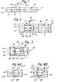
- the known dynode 10 comprises an apertured planar member having a plurality of re-entrant shaped, for example barrel-shaped, apertures 12 therein.
- the apertures 12 are generally symmetrical about their longitudinal axes and about a median plane through the dynode.
- the input and output cross-sections dl and d2 are substantially the same and less than a cross-section d3 within the aperture.
- the input/output cross-section dl or d2 of the apertures is usually equal to the thickness x of the dynode 10 and thus may be regarded as having a 1:1 aspect ratio.
- the cross-section dl and d2 300um and the pitch, P, of the apertures is 770pm.
- the material may be a known secondary emitting material such as a beryllium/copper alloy or a less expensive material such as mild steel which is a poor secondary emitter.
- a secondary emitting material such as magnesium oxide can be deposited in the apertures 12.
- each of the sheets 14, 16 will be 150pm.
- Such sheets can be handled reasonably easily and when a stack of dynodes is assembled with intervening spacers to form a laminated electron multiplier, the assembly is fairly rigid.
- the pitch P is smaller, and the input and output cross-sections dl and d2 may have to be smaller which in turn means that the thickness x is smaller.
- the cross-sections dl and d2 equal to 100 ⁇ m then if the 1:1 aspect ratio is maintained the thickness x is 100 ⁇ m requiring the sheets 14, 16 to be 50pm thick.
- Such sheets are difficult to handle.
- Figures 2 and 3 show two embodiments of dynodes 10 which can have a high resolution but which can be made of a thicker, easier to handle, sheet material.
- the profile of the apertures 12 is such that they comprise a convergent input portion 20, a divergent output portion 22 and a re-entrant intermediate portion 24.
- the necks 26, 28 formed between the intermediate portion 24 and the input and output portions 20, 22, respectively, have substantially the same cross-sections dl, d2 which are smaller than the cross-section d3 intermediate the necks 26, 28 but are substantially equal to the axial distance T between the necks 26, 28.
- the intermediate portion 24 in which the electron multiplication takes place maintains the 1:1 aspect ratio.
- each of the sheets 14, 16 undergoes double sided etching to form in this example a bi-convergent hole.
- the sheets 14, 16 are assembled back-to-back to form the dynode 10 as shown in Figure 2.
- the apertures thus formed are symmetrical about their medial internal cross-sectional plane. If the sheet material is a poor secondary emitter, for example mild steel, then prior to assembling the sheets 14, 16 a good secondary emitter, such as magnesium oxide, is deposited in at least the electron multiplying portion of the one of the two sheets having the output portion 22.
- the apertures 12 are coaxial about their respective longitudinal axes and their cross-sections at the surfaces of the dynode are substantially the same.
- the input output and intermediate portions 20, 22 and 24, respectively, have a substantially spherical or spheroidal form. However as shown in Figure 3, the intermediate portion 24 may have a different, circularly symmetrical re-entrant shape.
- Figures 4A and 4B illustrate two embodiments which are variants on the embodiment shown in Figure 2 in that the input and output portions 20, 22, respectively, are cylindrical, rather than tapered.
- the two embodiments differ from each other in that the axial length L of the input and output portions 20, 22, respectively, in Figure 4A is less than that of the corresponding portions in Figure 4B.
- Etching cylindrical holes in metal is generally difficult because the etchant tends to erode the side of a hole as it penetrates into the material. However this does not always occur in non-metallic materials and holes with a cylindrical portion communicating with a tapered portion can be etched in glass, such as Fotoform (Registered Trade Mark) glass, and then subsequently metallised to form a half dynode.
- glass such as Fotoform (Registered Trade Mark) glass
- Figure 5 illustrates an electron multiplier structure comprising a stack of dynodes of the type shown in Figure 2 together with an input dynode 30 having convergent apertures 32 and an output dynode 34 with divergent apertures 36.
- the input and output dynodes 30, 34 are typically half the thickness of the dynodes 10.
- the dynodes are separated from each other by spacing means which are less conductive than the dynodes and typically comprise insulating material.
- the spacing means comprise ballotini 38 or other discrete spacers which may be applied in the manner disclosed in published European Patent Specification 0 006 267 details of which are included by way of reference.
- a substantially constant potential difference is maintained in use between successive dynodes with the output dynode 34 being at the highest voltage.
- the precise voltage difference per stage is related to obtaining a satisfactory gain from each dynode.
- the gain is determined ultimately by the number of electrons which impinge on a dynode and produce secondary electrons which impinge on the next following dynode and so on. Not all the secondary electrons will impinge upon the secondary emitting surface of the next following dynode, some will pass through the aperture in the next following dynode and perhaps leave the electron multiplier.
- the proportion of the total number of secondary electrons which land on the secondary emitting surface of the next following dynode is determined by the axial length, T, of the re-entrant apertures, the axial length, L, of the input and output portions 20, 22 and the spacing, S, between adjacent dynodes as well as the voltage difference between successive dynodes. Consequently whilst it is true to say that electron multiplication will take place with different values of T, L, S and dynode voltage, not all such values will give an acceptable gain. Thus by experiment it has been found that an acceptable gain has been achieved by the following electron multipliers:
- Figure 6 illustrates an example of a cathode ray tube 40 including a channel electron multiplier 42.
- the tube 40 includes an electron gun 44 which produces an electron beam 46 which is scanned by electro-magnetic deflection means 48 over the input side of the electron multiplier 42.
- a cathodoluminescent screen 50 is provided on a faceplate 52 which is disposed approximately 10mm from the output side of the electron multiplier 42.
- An accelerating field is provided between the electron multiplier 42 and the screen 50.
- the electron multiplier may be used in other types of cathode ray tube including a flat cathode ray tube disclosed in published European Patent Specification 0 070 060. Also the electron multiplying structure may be used to amplify the current produced by a photocathode in a photomultiplier tube.
- the number of dynodes used in fabricating the electron multiplier depends on the desired overall gain of the multiplier, that is the smaller the overall gain, the fewer the number of dynodes and vice versa.
Landscapes
- Electron Tubes For Measurement (AREA)
- Electrodes For Cathode-Ray Tubes (AREA)
- Image-Pickup Tubes, Image-Amplification Tubes, And Storage Tubes (AREA)
- Vessels, Lead-In Wires, Accessory Apparatuses For Cathode-Ray Tubes (AREA)
Applications Claiming Priority (2)
| Application Number | Priority Date | Filing Date | Title |
|---|---|---|---|
| GB08403298A GB2154053A (en) | 1984-02-08 | 1984-02-08 | High resolution channel multiplier dynodes |
| GB8403298 | 1984-02-08 |
Publications (2)
| Publication Number | Publication Date |
|---|---|
| EP0151502A1 true EP0151502A1 (fr) | 1985-08-14 |
| EP0151502B1 EP0151502B1 (fr) | 1988-09-14 |
Family
ID=10556265
Family Applications (1)
| Application Number | Title | Priority Date | Filing Date |
|---|---|---|---|
| EP85200132A Expired EP0151502B1 (fr) | 1984-02-08 | 1985-02-07 | Tube à rayons cathodiques et multiplicateur d'électrons correspondant |
Country Status (9)
| Country | Link |
|---|---|
| US (1) | US4626736A (fr) |
| EP (1) | EP0151502B1 (fr) |
| JP (1) | JPH067457B2 (fr) |
| KR (1) | KR920003142B1 (fr) |
| CA (1) | CA1232005A (fr) |
| DD (1) | DD232787A5 (fr) |
| DE (1) | DE3565025D1 (fr) |
| ES (1) | ES540143A0 (fr) |
| GB (1) | GB2154053A (fr) |
Families Citing this family (9)
| Publication number | Priority date | Publication date | Assignee | Title |
|---|---|---|---|---|
| JP3434574B2 (ja) * | 1994-06-06 | 2003-08-11 | 浜松ホトニクス株式会社 | 電子増倍管 |
| US5618217A (en) * | 1995-07-25 | 1997-04-08 | Center For Advanced Fiberoptic Applications | Method for fabrication of discrete dynode electron multipliers |
| WO2000002227A1 (fr) * | 1998-07-01 | 2000-01-13 | Kabushiki Kaisha Toshiba | Detecteur d'images radiologiques |
| JP4246879B2 (ja) * | 2000-04-03 | 2009-04-02 | 浜松ホトニクス株式会社 | 電子増倍管及び光電子増倍管 |
| JP4108905B2 (ja) | 2000-06-19 | 2008-06-25 | 浜松ホトニクス株式会社 | ダイノードの製造方法及び構造 |
| SG139599A1 (en) * | 2006-08-08 | 2008-02-29 | Singapore Tech Dynamics Pte | Method and apparatus for treating water or wastewater or the like |
| US8606366B2 (en) | 2009-02-18 | 2013-12-10 | Syneron Medical Ltd. | Skin treatment apparatus for personal use and method for using same |
| KR101357364B1 (ko) * | 2011-06-03 | 2014-02-03 | 하마마츠 포토닉스 가부시키가이샤 | 전자 증배부 및 그것을 포함하는 광전자 증배관 |
| CN104269338B (zh) * | 2014-09-17 | 2016-04-06 | 中国工程物理研究院激光聚变研究中心 | 用于光电成像和信号增强的变孔径微通道板及其制作方法 |
Citations (3)
| Publication number | Priority date | Publication date | Assignee | Title |
|---|---|---|---|---|
| EP0006267A1 (fr) * | 1978-06-14 | 1980-01-09 | Philips Electronics Uk Limited | Procédé de fabrication d'une galette à canaux |
| FR2504728A1 (fr) * | 1981-04-24 | 1982-10-29 | Hyperelec | Dispositif multiplicateur d'electrons et application aux photomultiplicateurs |
| DE3318590A1 (de) * | 1982-06-16 | 1983-12-22 | N.V. Philips' Gloeilampenfabrieken, 5621 Eindhoven | Farbbildwiedergaberoehre |
Family Cites Families (4)
| Publication number | Priority date | Publication date | Assignee | Title |
|---|---|---|---|---|
| US4041343A (en) * | 1963-07-12 | 1977-08-09 | International Telephone And Telegraph Corporation | Electron multiplier mosaic |
| GB1434053A (en) * | 1973-04-06 | 1976-04-28 | Mullard Ltd | Electron multipliers |
| GB1446774A (en) * | 1973-04-19 | 1976-08-18 | Mullard Ltd | Electron beam devices incorporating electron multipliers |
| DE2844512C2 (de) * | 1978-10-12 | 1980-11-20 | Siemens Ag | Steuerplatte zur Matrixansteuerung einzelner Bildpunkte nach Zeile und Spalte auf einem Bildschirm in flachen Plasmabildwiedergabevorrichtungen |
-
1984
- 1984-02-08 GB GB08403298A patent/GB2154053A/en not_active Withdrawn
-
1985
- 1985-01-29 US US06/695,998 patent/US4626736A/en not_active Expired - Fee Related
- 1985-02-05 DD DD85273052A patent/DD232787A5/de not_active IP Right Cessation
- 1985-02-05 ES ES540143A patent/ES540143A0/es active Granted
- 1985-02-06 KR KR1019850000754A patent/KR920003142B1/ko not_active Expired
- 1985-02-06 JP JP60021594A patent/JPH067457B2/ja not_active Expired - Lifetime
- 1985-02-07 CA CA000473771A patent/CA1232005A/fr not_active Expired
- 1985-02-07 EP EP85200132A patent/EP0151502B1/fr not_active Expired
- 1985-02-07 DE DE8585200132T patent/DE3565025D1/de not_active Expired
Patent Citations (3)
| Publication number | Priority date | Publication date | Assignee | Title |
|---|---|---|---|---|
| EP0006267A1 (fr) * | 1978-06-14 | 1980-01-09 | Philips Electronics Uk Limited | Procédé de fabrication d'une galette à canaux |
| FR2504728A1 (fr) * | 1981-04-24 | 1982-10-29 | Hyperelec | Dispositif multiplicateur d'electrons et application aux photomultiplicateurs |
| DE3318590A1 (de) * | 1982-06-16 | 1983-12-22 | N.V. Philips' Gloeilampenfabrieken, 5621 Eindhoven | Farbbildwiedergaberoehre |
Also Published As
| Publication number | Publication date |
|---|---|
| US4626736A (en) | 1986-12-02 |
| ES8603111A1 (es) | 1985-12-01 |
| ES540143A0 (es) | 1985-12-01 |
| GB8403298D0 (en) | 1984-03-14 |
| JPS60182642A (ja) | 1985-09-18 |
| DE3565025D1 (en) | 1988-10-20 |
| KR850006248A (ko) | 1985-10-02 |
| KR920003142B1 (ko) | 1992-04-20 |
| EP0151502B1 (fr) | 1988-09-14 |
| DD232787A5 (de) | 1986-02-05 |
| CA1232005A (fr) | 1988-01-26 |
| JPH067457B2 (ja) | 1994-01-26 |
| GB2154053A (en) | 1985-08-29 |
Similar Documents
| Publication | Publication Date | Title |
|---|---|---|
| US4482836A (en) | Electron multipliers | |
| EP0690478A1 (fr) | Tube électronique | |
| US4041343A (en) | Electron multiplier mosaic | |
| EP0151502B1 (fr) | Tube à rayons cathodiques et multiplicateur d'électrons correspondant | |
| EP1313133B1 (fr) | Photomultiplicateur | |
| US4431943A (en) | Electron discharge device having a high speed cage | |
| GB2124017A (en) | A deflection colour selection system for a single beam channel plate display tube | |
| JPH05182631A (ja) | 電子増倍器を備えた電子管 | |
| US4886996A (en) | Channel plate electron multipliers | |
| US4980604A (en) | Sheet-type dynode electron multiplier and photomultiplier tube comprising such dynodes | |
| US4511822A (en) | Image display tube having a channel plate electron multiplier | |
| US4227116A (en) | Zero-bias gridded gun | |
| US5043628A (en) | Fast photomultiplier tube having a high collection homogeneity | |
| US4544860A (en) | Laminated channel plate electron multiplier | |
| EP0349081A1 (fr) | Tube électronique | |
| US4626737A (en) | Mask focusing color picture tube | |
| US2200722A (en) | Electron discharge device | |
| US4893053A (en) | Color display tube with channel electron multiplier means | |
| US3182221A (en) | Secondary emission multiplier structure | |
| US3849644A (en) | Electron discharge device having ellipsoid-shaped electrode surfaces | |
| US4792718A (en) | Cathode ray display tubes | |
| US3716738A (en) | Television camera tube having channel multiplier surrounding electron gun | |
| EP0131336A1 (fr) | Tube à rayons cathodiques | |
| EP0131335A1 (fr) | Tube à rayons cathodiques | |
| Knapp et al. | Large-area channel electron multiplier for CRT applications |
Legal Events
| Date | Code | Title | Description |
|---|---|---|---|
| PUAI | Public reference made under article 153(3) epc to a published international application that has entered the european phase |
Free format text: ORIGINAL CODE: 0009012 |
|
| AK | Designated contracting states |
Designated state(s): DE FR GB IT NL SE |
|
| 17P | Request for examination filed |
Effective date: 19860109 |
|
| 17Q | First examination report despatched |
Effective date: 19870706 |
|
| RAP3 | Party data changed (applicant data changed or rights of an application transferred) |
Owner name: N.V. PHILIPS' GLOEILAMPENFABRIEKEN Owner name: PHILIPS ELECTRONIC AND ASSOCIATED INDUSTRIES LIMIT |
|
| GRAA | (expected) grant |
Free format text: ORIGINAL CODE: 0009210 |
|
| AK | Designated contracting states |
Kind code of ref document: B1 Designated state(s): DE FR GB IT NL SE |
|
| REF | Corresponds to: |
Ref document number: 3565025 Country of ref document: DE Date of ref document: 19881020 |
|
| ITF | It: translation for a ep patent filed | ||
| ET | Fr: translation filed | ||
| PGFP | Annual fee paid to national office [announced via postgrant information from national office to epo] |
Ref country code: SE Payment date: 19890224 Year of fee payment: 5 |
|
| ITTA | It: last paid annual fee | ||
| PGFP | Annual fee paid to national office [announced via postgrant information from national office to epo] |
Ref country code: NL Payment date: 19890228 Year of fee payment: 5 |
|
| PLBE | No opposition filed within time limit |
Free format text: ORIGINAL CODE: 0009261 |
|
| STAA | Information on the status of an ep patent application or granted ep patent |
Free format text: STATUS: NO OPPOSITION FILED WITHIN TIME LIMIT |
|
| 26N | No opposition filed | ||
| PG25 | Lapsed in a contracting state [announced via postgrant information from national office to epo] |
Ref country code: SE Effective date: 19900208 |
|
| PG25 | Lapsed in a contracting state [announced via postgrant information from national office to epo] |
Ref country code: NL Effective date: 19900901 |
|
| NLV4 | Nl: lapsed or anulled due to non-payment of the annual fee | ||
| EUG | Se: european patent has lapsed |
Ref document number: 85200132.0 Effective date: 19901107 |
|
| REG | Reference to a national code |
Ref country code: FR Ref legal event code: CD |
|
| PGFP | Annual fee paid to national office [announced via postgrant information from national office to epo] |
Ref country code: DE Payment date: 19960424 Year of fee payment: 12 |
|
| PGFP | Annual fee paid to national office [announced via postgrant information from national office to epo] |
Ref country code: GB Payment date: 19970203 Year of fee payment: 13 |
|
| PGFP | Annual fee paid to national office [announced via postgrant information from national office to epo] |
Ref country code: FR Payment date: 19970218 Year of fee payment: 13 |
|
| PG25 | Lapsed in a contracting state [announced via postgrant information from national office to epo] |
Ref country code: DE Effective date: 19971101 |
|
| PG25 | Lapsed in a contracting state [announced via postgrant information from national office to epo] |
Ref country code: GB Free format text: LAPSE BECAUSE OF NON-PAYMENT OF DUE FEES Effective date: 19980207 |
|
| PG25 | Lapsed in a contracting state [announced via postgrant information from national office to epo] |
Ref country code: FR Free format text: THE PATENT HAS BEEN ANNULLED BY A DECISION OF A NATIONAL AUTHORITY Effective date: 19980228 |
|
| GBPC | Gb: european patent ceased through non-payment of renewal fee |
Effective date: 19980207 |
|
| REG | Reference to a national code |
Ref country code: FR Ref legal event code: ST |