EP0152326A2 - Herstellungsverfahren eines Schreib- und Lesemagnetkopfes - Google Patents
Herstellungsverfahren eines Schreib- und Lesemagnetkopfes Download PDFInfo
- Publication number
- EP0152326A2 EP0152326A2 EP85400136A EP85400136A EP0152326A2 EP 0152326 A2 EP0152326 A2 EP 0152326A2 EP 85400136 A EP85400136 A EP 85400136A EP 85400136 A EP85400136 A EP 85400136A EP 0152326 A2 EP0152326 A2 EP 0152326A2
- Authority
- EP
- European Patent Office
- Prior art keywords
- layer
- magnetic
- groove
- pole pieces
- wall
- Prior art date
- Legal status (The legal status is an assumption and is not a legal conclusion. Google has not performed a legal analysis and makes no representation as to the accuracy of the status listed.)
- Granted
Links
Images


Classifications
-
- G—PHYSICS
- G11—INFORMATION STORAGE
- G11B—INFORMATION STORAGE BASED ON RELATIVE MOVEMENT BETWEEN RECORD CARRIER AND TRANSDUCER
- G11B5/00—Recording by magnetisation or demagnetisation of a record carrier; Reproducing by magnetic means; Record carriers therefor
- G11B5/127—Structure or manufacture of heads, e.g. inductive
- G11B5/31—Structure or manufacture of heads, e.g. inductive using thin films
- G11B5/3176—Structure of heads comprising at least in the transducing gap regions two magnetic thin films disposed respectively at both sides of the gaps
- G11B5/3179—Structure of heads comprising at least in the transducing gap regions two magnetic thin films disposed respectively at both sides of the gaps the films being mainly disposed in parallel planes
- G11B5/3183—Structure of heads comprising at least in the transducing gap regions two magnetic thin films disposed respectively at both sides of the gaps the films being mainly disposed in parallel planes intersecting the gap plane, e.g. "horizontal head structure"
-
- G—PHYSICS
- G11—INFORMATION STORAGE
- G11B—INFORMATION STORAGE BASED ON RELATIVE MOVEMENT BETWEEN RECORD CARRIER AND TRANSDUCER
- G11B5/00—Recording by magnetisation or demagnetisation of a record carrier; Reproducing by magnetic means; Record carriers therefor
- G11B5/127—Structure or manufacture of heads, e.g. inductive
-
- G—PHYSICS
- G11—INFORMATION STORAGE
- G11B—INFORMATION STORAGE BASED ON RELATIVE MOVEMENT BETWEEN RECORD CARRIER AND TRANSDUCER
- G11B5/00—Recording by magnetisation or demagnetisation of a record carrier; Reproducing by magnetic means; Record carriers therefor
- G11B5/127—Structure or manufacture of heads, e.g. inductive
- G11B5/17—Construction or disposition of windings
-
- G—PHYSICS
- G11—INFORMATION STORAGE
- G11B—INFORMATION STORAGE BASED ON RELATIVE MOVEMENT BETWEEN RECORD CARRIER AND TRANSDUCER
- G11B5/00—Recording by magnetisation or demagnetisation of a record carrier; Reproducing by magnetic means; Record carriers therefor
- G11B5/127—Structure or manufacture of heads, e.g. inductive
- G11B5/31—Structure or manufacture of heads, e.g. inductive using thin films
- G11B5/3103—Structure or manufacture of integrated heads or heads mechanically assembled and electrically connected to a support or housing
- G11B5/3106—Structure or manufacture of integrated heads or heads mechanically assembled and electrically connected to a support or housing where the integrated or assembled structure comprises means for conditioning against physical detrimental influence, e.g. wear, contamination
-
- Y—GENERAL TAGGING OF NEW TECHNOLOGICAL DEVELOPMENTS; GENERAL TAGGING OF CROSS-SECTIONAL TECHNOLOGIES SPANNING OVER SEVERAL SECTIONS OF THE IPC; TECHNICAL SUBJECTS COVERED BY FORMER USPC CROSS-REFERENCE ART COLLECTIONS [XRACs] AND DIGESTS
- Y10—TECHNICAL SUBJECTS COVERED BY FORMER USPC
- Y10T—TECHNICAL SUBJECTS COVERED BY FORMER US CLASSIFICATION
- Y10T29/00—Metal working
- Y10T29/49—Method of mechanical manufacture
- Y10T29/49002—Electrical device making
- Y10T29/4902—Electromagnet, transformer or inductor
- Y10T29/49021—Magnetic recording reproducing transducer [e.g., tape head, core, etc.]
- Y10T29/49032—Fabricating head structure or component thereof
- Y10T29/49036—Fabricating head structure or component thereof including measuring or testing
- Y10T29/49043—Depositing magnetic layer or coating
- Y10T29/49044—Plural magnetic deposition layers
-
- Y—GENERAL TAGGING OF NEW TECHNOLOGICAL DEVELOPMENTS; GENERAL TAGGING OF CROSS-SECTIONAL TECHNOLOGIES SPANNING OVER SEVERAL SECTIONS OF THE IPC; TECHNICAL SUBJECTS COVERED BY FORMER USPC CROSS-REFERENCE ART COLLECTIONS [XRACs] AND DIGESTS
- Y10—TECHNICAL SUBJECTS COVERED BY FORMER USPC
- Y10T—TECHNICAL SUBJECTS COVERED BY FORMER US CLASSIFICATION
- Y10T29/00—Metal working
- Y10T29/49—Method of mechanical manufacture
- Y10T29/49002—Electrical device making
- Y10T29/4902—Electromagnet, transformer or inductor
- Y10T29/49021—Magnetic recording reproducing transducer [e.g., tape head, core, etc.]
- Y10T29/49032—Fabricating head structure or component thereof
- Y10T29/49036—Fabricating head structure or component thereof including measuring or testing
- Y10T29/49043—Depositing magnetic layer or coating
- Y10T29/49046—Depositing magnetic layer or coating with etching or machining of magnetic material
-
- Y—GENERAL TAGGING OF NEW TECHNOLOGICAL DEVELOPMENTS; GENERAL TAGGING OF CROSS-SECTIONAL TECHNOLOGIES SPANNING OVER SEVERAL SECTIONS OF THE IPC; TECHNICAL SUBJECTS COVERED BY FORMER USPC CROSS-REFERENCE ART COLLECTIONS [XRACs] AND DIGESTS
- Y10—TECHNICAL SUBJECTS COVERED BY FORMER USPC
- Y10T—TECHNICAL SUBJECTS COVERED BY FORMER US CLASSIFICATION
- Y10T29/00—Metal working
- Y10T29/49—Method of mechanical manufacture
- Y10T29/49002—Electrical device making
- Y10T29/4902—Electromagnet, transformer or inductor
- Y10T29/49021—Magnetic recording reproducing transducer [e.g., tape head, core, etc.]
- Y10T29/49032—Fabricating head structure or component thereof
- Y10T29/4906—Providing winding
- Y10T29/49064—Providing winding by coating
Definitions
- the subject of the present invention is a method for producing a magnetic writing and titer head and a head obtained by this method. It finds an application in magnetic recording equipment and in particular in computer memories.
- the magnetic head which is the subject of the present invention is of the type which comprises two pole pieces, a double spiral flat coil winding surrounding each of these pole pieces, and an air gap filled with a non-magnetic layer, the latter flush with a surface plane which constitutes what is called the head plane.
- the magnetic recording medium moves relatively to the head in front of the air gap, parallel to the flight plan.
- a current flowing in the winding causes a magnetic field at the air gap which causes the writing information in the support.
- magnetic information written on the moving support induces a field in the pole pieces, therefore a current in the winding and a voltage across its terminals which constitutes a measurement signal.
- As the magnetic field involved in these writing and reading operations is parallel to the recording medium, we sometimes speak of horizontal magnetic recording.
- Such a head is described for example in Japanese patent publication No. 56 83823 filed by FUJITSU KK for "Production for Horizontal Thin Film Magnetic Head", the abstract of which was published in Patent Abstracts of Japan vol 5, No. 150 (P-81) (822) September 22, 1981.
- the method of manufacturing such a head consists in bonding end to end two fine magnetic parts on a substrate, these magnetic parts being separated by a non-magnetic layer defining the air gap. This assembly is then machined to reduce the height of the air gap. Separately, a support is constituted comprising a double winding surrounding two pole pieces. These two subsets are then glued to each other.
- Such a method has many drawbacks. First of all, it requires delicate assembly of small parts, which makes it not very compatible with industrial and automated processes. Then, the writing and reading pole pieces have a width, on the one hand, large, which harms the efficiency of the head and, on the other hand, not very reproducible, which leads to dispersions in the performances. Finally, the winding can induce stray fields in the recording layer.
- the present invention relates to a method of producing a magnetic head which overcomes these drawbacks. Using thin film technology operations, this process lends itself perfectly to automation. Then, the width of the writing and reading pole pieces is found to be defined by the thickness of a thin layer, so that this thickness is small and perfectly reproducible. Finally, the conductive winding is inserted between two magnetic layers and is therefore completely shielded.
- the present invention also relates to a magnetic head which is obtained by the method which has just been defined.
- This head is characterized by the presence of two magnetic layers which completely enclose the spiral winding and by the fact that the writing and reading pole pieces are constituted by sections of a thin magnetic layer.
- the support 20 can be either a ceramic, a dielectric, or a silicon wafer similar to that used in semiconductor technology.
- the wafer is coated with a layer of silica 22 which is grown by thermal oxidation.
- a layer 24 is then deposited using a magnetic material with high permeability and strong magnetization, such as a ferrite or an alloy of FeNi or Co, Zr, Nb. The thickness of this magnetic layer is between 0.5 ⁇ m and 5 ⁇ m.
- Figures 2 and 3 show an eight-shaped groove 26 etched in Layer 24. The etching of this groove leaves two central pole pieces 26a and 26b separated by a straight central channel 26c. This groove 26 is obtained using a resin mask produced by photolithography and etched either chemically or by dry etching.
- the engraving depth of the groove 26 corresponds to a fraction of the thickness of the layer 24 (one third or one half).
- FIG. 4 shows the filling of the groove 26 with a dielectric material 27 such as silica or resin.
- a dielectric material 27 such as silica or resin.
- a double spiral groove 28 and 30 is then made in the filling dielectric 27 (FIG. 4)
- a layer of an electrically conductive material 31 is then deposited at the bottom of this double groove.
- This material can be copper or aluminum.
- a winding is thus constituted, the plane of which is parallel to the recording layer. The winding comprises a half 28 surrounding the pole piece 26a and a half 30 surrounding the pole piece 26b.
- the two grooves 28 and 30 are then filled with an insulating material similar or identical to the material 27.
- a dielectric layer 32 is then deposited on the assembly.
- This layer preferably consists of a photosensitive resin. Its thickness is between 0.5 ⁇ m and a few microns.
- a step is practiced, the flank 33 of which is offset with respect to the axis of the central channel 26c separating the poles 26a and 26b. This offset is approximately equal to the half thickness of the non-magnetic layer 34 which is then deposited.
- This non-magnetic layer is advantageously silica or alulumine and it covers the step with resin, as shown in FIG. 7.
- a magnetic layer 36 is then deposited, which can be of the same nature as The layer 24.
- This layer 36 forms a boss at the level of the wall 34a, as can be seen in FIG. 8.
- a layer is then deposited on the assembly. of hard insulating protection 38, which can be in sitice or in alumina. This layer marries Boss 37.
- a layer of resin 40 is deposited which will temporarily serve to cut the bosses and the wall 34a. The sectioning is carried out in layer 38.
- the top of the wall 34a is then uncovered, thus producing an air gap located between the two pole pieces 36a and 36b.
- the magnetic layer 36 has a thickness of between 0.2 and 1.5 ⁇ m. It is therefore very thin. This is the case with the pole pieces 36a and 36b, the width of which is of the same order as this thickness. This is what gives the magnetic head of the invention a high efficiency.
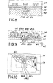
- FIG. 9 represents the head finally obtained.
- the arrows schematize the lines of flow in writing in a magnetic support 42 moving opposite the flight plan 41 constituted by what remains of the layer 38.
- the two lateral parts of the winding are magnetically shielded by the two layers 24 and 36 and therefore do not produce any leakage field towards the recording layer 42.
- Figure 10 shows an exploded view of the head observed in front of its flight plan. Only the ends of the two pole pieces 36a, 36b of writing and reading separated by the wall 34a are flush with the level of the flight plan.
Landscapes
- Engineering & Computer Science (AREA)
- Manufacturing & Machinery (AREA)
- Magnetic Heads (AREA)
Applications Claiming Priority (2)
| Application Number | Priority Date | Filing Date | Title |
|---|---|---|---|
| FR8401879 | 1984-02-03 | ||
| FR8401879A FR2559293B1 (fr) | 1984-02-03 | 1984-02-03 | Nouvelle tete magnetique d'ecriture et de lecture pour enregistrement magnetique et son procede de fabrication |
Publications (3)
| Publication Number | Publication Date |
|---|---|
| EP0152326A2 true EP0152326A2 (de) | 1985-08-21 |
| EP0152326A3 EP0152326A3 (en) | 1985-09-18 |
| EP0152326B1 EP0152326B1 (de) | 1989-08-09 |
Family
ID=9300842
Family Applications (1)
| Application Number | Title | Priority Date | Filing Date |
|---|---|---|---|
| EP85400136A Expired EP0152326B1 (de) | 1984-02-03 | 1985-01-28 | Herstellungsverfahren eines Schreib- und Lesemagnetkopfes |
Country Status (5)
| Country | Link |
|---|---|
| US (2) | US4639289A (de) |
| EP (1) | EP0152326B1 (de) |
| JP (1) | JPH0644333B2 (de) |
| DE (1) | DE3572237D1 (de) |
| FR (1) | FR2559293B1 (de) |
Families Citing this family (48)
| Publication number | Priority date | Publication date | Assignee | Title |
|---|---|---|---|---|
| FR2586851B1 (fr) * | 1985-09-04 | 1989-09-22 | Commissariat Energie Atomique | Procede de realisation d'une tete magnetique horizontale enterree et tete magnetique obtenue par ce procede |
| EP0218445A3 (de) * | 1985-10-01 | 1989-08-30 | Sony Corporation | Dünnfilmmagnetköpfe |
| FR2604021B1 (fr) * | 1986-09-17 | 1988-10-28 | Commissariat Energie Atomique | Procede de realisation de tetes magnetiques en couches minces et a structure planaire et tete obtenue par ce procede |
| FR2606197B1 (fr) * | 1986-10-31 | 1988-12-02 | Commissariat Energie Atomique | Procede de realisation d'une tete magnetique permettant de simplifier la realisation des connexions electriques |
| US5159511A (en) * | 1987-04-01 | 1992-10-27 | Digital Equipment Corporation | Biasing conductor for MR head |
| US4985985A (en) * | 1987-07-01 | 1991-01-22 | Digital Equipment Corporation | Solenoidal thin film read/write head for computer mass storage device and method of making same |
| US4972287A (en) * | 1987-07-01 | 1990-11-20 | Digital Equipment Corp. | Having a solenoidal energizing coil |
| FR2622336B1 (fr) * | 1987-10-27 | 1995-07-21 | Europ Composants Electron | Tete magnetique de lecture et d'enregistrement |
| US4912584A (en) * | 1988-03-09 | 1990-03-27 | Digital Equipment Corporation | Method for fabricating magnetic recording poles |
| FR2645315B1 (fr) * | 1989-03-29 | 1991-05-31 | Commissariat Energie Atomique | Tete magnetique de lecture a magnetoresistance pour enregistrement perpendiculaire et procede de realisation d'une telle tete |
| FR2645314B1 (fr) * | 1989-03-29 | 1991-05-31 | Commissariat Energie Atomique | Tete magnetique a magnetoresistance pour enregistrement longitudinal et procede de realisation d'une telle tete |
| US5189580A (en) * | 1989-06-30 | 1993-02-23 | Ampex Corporation | Ultra small track width thin film magnetic transducer |
| FR2650127B1 (fr) * | 1989-07-18 | 1991-09-20 | Thomson Csf | Generateur d'impulsion laser de puissance |
| US5155643A (en) * | 1990-10-30 | 1992-10-13 | Mars Incorporated | Unshielded horizontal magnetoresistive head and method of fabricating same |
| US5173826A (en) * | 1991-06-03 | 1992-12-22 | Read-Rite Corp. | Thin film head with coils of varying thickness |
| US5472736A (en) * | 1991-06-03 | 1995-12-05 | Read-Rite Corporation | Method of making a bi-level coil for a thin film magnetic transducer |
| US5378885A (en) * | 1991-10-29 | 1995-01-03 | Mars Incorporated | Unshielded magnetoresistive head with multiple pairs of sensing elements |
| FR2709855B1 (fr) * | 1993-09-06 | 1995-10-20 | Commissariat Energie Atomique | Tête magnétique de lecture et d'écriture à élément magnétorésistant compensé en écriture. |
| US5452166A (en) * | 1993-10-01 | 1995-09-19 | Applied Magnetics Corporation | Thin film magnetic recording head for minimizing undershoots and a method for manufacturing the same |
| US5781379A (en) * | 1994-03-15 | 1998-07-14 | International Business Machines Corporation | Single beam flexure for a head gimbal assembly |
| US6351348B1 (en) | 1994-03-15 | 2002-02-26 | International Business Machines Corporation | Minimal stiffness conductors for a head gimbal assembly |
| US6282064B1 (en) | 1994-03-15 | 2001-08-28 | International Business Machines Corporation | Head gimbal assembly with integrated electrical conductors |
| US5801909A (en) * | 1994-08-26 | 1998-09-01 | Aiwa Research And Development, Inc. | Thin film magnetic head including durable wear layer and non-magnetic gap structures |
| US5673474A (en) * | 1994-08-26 | 1997-10-07 | Aiwa Research And Development, Inc. | Method of fabricating a thin film magnetic head including layered magnetic side poles |
| US5909346A (en) * | 1994-08-26 | 1999-06-01 | Aiwa Research & Development, Inc. | Thin magnetic film including multiple geometry gap structures on a common substrate |
| US5544774A (en) * | 1994-08-26 | 1996-08-13 | Aiwa Research And Development, Inc. | Method of eliminating pole recession in a thin film magnetic head |
| US6091581A (en) * | 1994-08-26 | 2000-07-18 | Aiwa Co., Ltd. | Thin film magnetic head including a separately deposited diamond-like carbon gap structure and magnetic control wells |
| US5563754A (en) * | 1994-08-26 | 1996-10-08 | Aiwa Research And Development, Inc. | Thin film magnetic head including a durable wear layer and gap structure |
| US5754377A (en) * | 1994-08-26 | 1998-05-19 | Aiwa Research And Development, Inc. | Thin film magnetic head including an elevated gap structure |
| US5748417A (en) * | 1994-08-26 | 1998-05-05 | Aiwa Research And Development, Inc. | Thin film magnetic head including layered magnetic side poles |
| JPH08171712A (ja) * | 1994-08-26 | 1996-07-02 | Aiwa Co Ltd | 側面露出型薄膜磁気ヘッド並びにその製造方法 |
| US5490028A (en) * | 1994-08-26 | 1996-02-06 | Aiwa Research And Development, Inc. | Thin film magnetic head including an integral layered shield structure |
| FR2727778B1 (fr) * | 1994-12-02 | 1997-01-03 | Commissariat Energie Atomique | Codeur magnetique pour la lecture de marques sur une piste magnetique associee |
| US5621594A (en) * | 1995-02-17 | 1997-04-15 | Aiwa Research And Development, Inc. | Electroplated thin film conductor coil assembly |
| JPH0916925A (ja) * | 1995-06-28 | 1997-01-17 | Yamaha Corp | 誘導型・mr型複合磁気ヘッドおよびその製造方法 |
| US5742452A (en) * | 1996-01-10 | 1998-04-21 | International Business Machines Corporation | Low mass magnetic recording head and suspension |
| US6069015A (en) * | 1996-05-20 | 2000-05-30 | Aiwa Research And Development, Inc. | Method of fabricating thin film magnetic head including durable wear layer and non-magnetic gap structure |
| US5768070A (en) | 1997-05-14 | 1998-06-16 | International Business Machines Corporation | Horizontal thin film write, MR read head |
| KR100264802B1 (ko) | 1998-02-24 | 2000-09-01 | 윤종용 | 플래너구조 박막자기헤드의 갭 형성방법 |
| US5871655A (en) * | 1998-03-19 | 1999-02-16 | International Business Machines Corporation | Integrated conductor magnetic recording head and suspension having cross-over integrated circuits for noise reduction |
| US6055138A (en) * | 1998-05-06 | 2000-04-25 | Read-Rite Corporation | Thin film pedestal pole tips write head having narrower lower pedestal pole tip |
| US6944938B1 (en) | 1999-05-03 | 2005-09-20 | Western Digital (Fremont), Inc. | Method of forming a magnetoresistive device |
| US6829819B1 (en) | 1999-05-03 | 2004-12-14 | Western Digital (Fremont), Inc. | Method of forming a magnetoresistive device |
| US6396660B1 (en) * | 1999-08-23 | 2002-05-28 | Read-Rite Corporation | Magnetic write element having a thermally dissipative structure |
| US6452742B1 (en) | 1999-09-02 | 2002-09-17 | Read-Rite Corporation | Thin film write having reduced resistance conductor coil partially recessed within middle coat insulation |
| US6861937B1 (en) | 2002-06-25 | 2005-03-01 | Western Digital (Fremont), Inc. | Double winding twin coil for thin-film head writer |
| JP2004087024A (ja) * | 2002-08-28 | 2004-03-18 | Shinka Jitsugyo Kk | 薄膜磁気ヘッド |
| US8427780B2 (en) * | 2009-01-23 | 2013-04-23 | International Business Machines Corporation | Planar magnetic writer having offset portions |
Family Cites Families (11)
| Publication number | Priority date | Publication date | Assignee | Title |
|---|---|---|---|---|
| DE2547792C3 (de) * | 1974-10-25 | 1978-08-31 | Hitachi, Ltd., Tokio | Verfahren zur Herstellung eines Halbleiterbauelementes |
| SU662961A1 (ru) * | 1976-12-06 | 1979-05-15 | Предприятие П/Я А-3759 | Тонкопленочна магнитна головка |
| JPS54157613A (en) * | 1978-06-02 | 1979-12-12 | Fujitsu Ltd | Magnetic head |
| US4256514A (en) * | 1978-11-03 | 1981-03-17 | International Business Machines Corporation | Method for forming a narrow dimensioned region on a body |
| JPS55105817A (en) * | 1979-02-01 | 1980-08-13 | Fujitsu Ltd | Thin-film magnetic head |
| JPS55132519A (en) * | 1979-04-03 | 1980-10-15 | Fujitsu Ltd | Manufacture for thin film magnetic head |
| JPS55135321A (en) * | 1979-04-10 | 1980-10-22 | Fujitsu Ltd | Manufacture of thin-film magnetic head |
| JPS5674812A (en) * | 1979-11-26 | 1981-06-20 | Nippon Telegr & Teleph Corp <Ntt> | Magnetic head assembly |
| JPS5683823A (en) * | 1979-12-11 | 1981-07-08 | Fujitsu Ltd | Production for horizontal thin film magnetic head |
| JPS56145517A (en) * | 1980-04-14 | 1981-11-12 | Fujitsu Ltd | Thin-film magnetic head |
| JPS5798118A (en) * | 1980-12-08 | 1982-06-18 | Fujitsu Ltd | Method for manufacturing magnetic head |
-
1984
- 1984-02-03 FR FR8401879A patent/FR2559293B1/fr not_active Expired
-
1985
- 1985-01-28 EP EP85400136A patent/EP0152326B1/de not_active Expired
- 1985-01-28 DE DE8585400136T patent/DE3572237D1/de not_active Expired
- 1985-01-30 US US06/696,517 patent/US4639289A/en not_active Ceased
- 1985-02-04 JP JP60018785A patent/JPH0644333B2/ja not_active Expired - Lifetime
-
1989
- 1989-01-24 US US07/300,974 patent/USRE33383E/en not_active Expired - Lifetime
Also Published As
| Publication number | Publication date |
|---|---|
| JPH0644333B2 (ja) | 1994-06-08 |
| FR2559293B1 (fr) | 1988-09-09 |
| JPS60179917A (ja) | 1985-09-13 |
| FR2559293A1 (fr) | 1985-08-09 |
| USRE33383E (en) | 1990-10-16 |
| EP0152326A3 (en) | 1985-09-18 |
| DE3572237D1 (en) | 1989-09-14 |
| US4639289A (en) | 1987-01-27 |
| EP0152326B1 (de) | 1989-08-09 |
Similar Documents
| Publication | Publication Date | Title |
|---|---|---|
| EP0152326B1 (de) | Herstellungsverfahren eines Schreib- und Lesemagnetkopfes | |
| EP0153886B1 (de) | Herstellungsverfahren eines Magnetkopfes für senkrechte Aufzeichnung | |
| EP0262028B1 (de) | Herstellungsverfahren von Dünnfilm-Magnetköpfen mit Planarstruktur und nach diesem Verfahren hergestellter Kopf | |
| EP0152325B1 (de) | Herstellungsverfahren einer Wicklung für Aufnahmemagnetkopf und Wicklung hergestellt nach diesem Verfahren | |
| EP0420755B1 (de) | Herstellungsverfahren eines Magnetaufzeichnungskopfes und nach diesem Verfahren erhaltener Kopf | |
| FR2726960A1 (fr) | Procede de realisation de transducteurs magnetoresistifs | |
| FR2813987A1 (fr) | Microcomposant du type micro-inductance ou micro-transformateur | |
| CA2308871A1 (fr) | Micro-composants du type micro-inductance ou micro-transformateur, et procede de fabrication de tels micro-composants | |
| EP0284495B1 (de) | Magnetkopf zum Lesen von Spuren mit sehr schmaler Breite und Herstellungverfahren | |
| FR2605783A1 (fr) | T ete magnetique d'enregistrement/lecture en couches minces et son procede de realisation | |
| FR2645315A1 (fr) | Tete magnetique de lecture a magnetoresistance pour enregistrement perpendiculaire et procede de realisation d'une telle tete | |
| FR2630244A1 (fr) | Dispositif d'ecriture et de lecture sur un support magnetique et son procede de fabrication | |
| EP0406362B1 (de) | Herstellungsverfahren eines aufnahme-/wiedergabekopfes und nach diesem verfahren erhaltener kopf | |
| EP0452193B1 (de) | Herstellungsverfahren von einem magnetischen Wiedergabe-Aufzeichnungskopf | |
| EP0304373B1 (de) | Verfahren zur Herstellung, eines Motivs, insbesondere aus ferromagnetischem Material mit Flanken von verschiedener Steilheit, und Magnetkopf mit einem solchen Motiv | |
| EP0644528B1 (de) | Aufzeichnungs- und Wiedergabemagnetkopf mit bezüglich Aufzeichnung kompensiertem Magnetowiderstandselement | |
| EP0338063B1 (de) | Aufzeichnungs-wiedergabemagnetkopf und verfahren zu seiner herstellung | |
| EP0219370B1 (de) | Herstellungsverfahren eines horizontal vergrabenen Magnetkopfes und nach diesem Verfahren hergestellter Magnetkopf | |
| EP0416994A1 (de) | Herstellungsverfahren eines Magnetkopfes mit passend orientierter Achse mit leichter Magnetisierung und nach diesem Verfahren hergestellter Kopf | |
| EP0367880B1 (de) | Herstellungsverfahren eines Aufzeichnungs-/Wiedergabemagnetkopfes | |
| FR2622336A1 (fr) | Tete magnetique de lecture et d'enregistrement | |
| EP0348265A1 (de) | Herstellungsverfahren eines Aufzeichnungs-Wiedergabemagnetkopfes aus einem magnetischen Substrat | |
| EP0811966A1 (de) | Magnetaufzeichnungs- und -wiedergabekopf mit Halbleiter-Feldsensor | |
| KR19990056467A (ko) | 평탄화 공정을 포함한 전도층 패턴 형성방법 | |
| FR2688513A1 (fr) | Procede de realisation d'une tete magnetique de type perpendiculaire et tete obtenue par ce procede. |
Legal Events
| Date | Code | Title | Description |
|---|---|---|---|
| PUAI | Public reference made under article 153(3) epc to a published international application that has entered the european phase |
Free format text: ORIGINAL CODE: 0009012 |
|
| PUAL | Search report despatched |
Free format text: ORIGINAL CODE: 0009013 |
|
| AK | Designated contracting states |
Designated state(s): BE CH DE FR GB IT LI NL |
|
| AK | Designated contracting states |
Designated state(s): BE CH DE FR GB IT LI NL |
|
| 17P | Request for examination filed |
Effective date: 19860227 |
|
| RAP1 | Party data changed (applicant data changed or rights of an application transferred) |
Owner name: COMMISSARIAT A L'ENERGIE ATOMIQUE |
|
| 17Q | First examination report despatched |
Effective date: 19880422 |
|
| GRAA | (expected) grant |
Free format text: ORIGINAL CODE: 0009210 |
|
| AK | Designated contracting states |
Kind code of ref document: B1 Designated state(s): BE CH DE FR GB IT LI NL |
|
| REF | Corresponds to: |
Ref document number: 3572237 Country of ref document: DE Date of ref document: 19890914 |
|
| ITF | It: translation for a ep patent filed | ||
| GBT | Gb: translation of ep patent filed (gb section 77(6)(a)/1977) | ||
| PLBE | No opposition filed within time limit |
Free format text: ORIGINAL CODE: 0009261 |
|
| STAA | Information on the status of an ep patent application or granted ep patent |
Free format text: STATUS: NO OPPOSITION FILED WITHIN TIME LIMIT |
|
| 26N | No opposition filed | ||
| ITTA | It: last paid annual fee | ||
| REG | Reference to a national code |
Ref country code: GB Ref legal event code: IF02 |
|
| PGFP | Annual fee paid to national office [announced via postgrant information from national office to epo] |
Ref country code: CH Payment date: 20020125 Year of fee payment: 18 |
|
| PGFP | Annual fee paid to national office [announced via postgrant information from national office to epo] |
Ref country code: FR Payment date: 20020128 Year of fee payment: 18 |
|
| PGFP | Annual fee paid to national office [announced via postgrant information from national office to epo] |
Ref country code: GB Payment date: 20020130 Year of fee payment: 18 |
|
| PGFP | Annual fee paid to national office [announced via postgrant information from national office to epo] |
Ref country code: NL Payment date: 20020131 Year of fee payment: 18 |
|
| PGFP | Annual fee paid to national office [announced via postgrant information from national office to epo] |
Ref country code: BE Payment date: 20020320 Year of fee payment: 18 |
|
| PGFP | Annual fee paid to national office [announced via postgrant information from national office to epo] |
Ref country code: DE Payment date: 20020326 Year of fee payment: 18 |
|
| PG25 | Lapsed in a contracting state [announced via postgrant information from national office to epo] |
Ref country code: GB Free format text: LAPSE BECAUSE OF NON-PAYMENT OF DUE FEES Effective date: 20030128 |
|
| PG25 | Lapsed in a contracting state [announced via postgrant information from national office to epo] |
Ref country code: LI Free format text: LAPSE BECAUSE OF NON-PAYMENT OF DUE FEES Effective date: 20030131 Ref country code: CH Free format text: LAPSE BECAUSE OF NON-PAYMENT OF DUE FEES Effective date: 20030131 Ref country code: BE Free format text: LAPSE BECAUSE OF NON-PAYMENT OF DUE FEES Effective date: 20030131 |
|
| PG25 | Lapsed in a contracting state [announced via postgrant information from national office to epo] |
Ref country code: NL Free format text: LAPSE BECAUSE OF NON-PAYMENT OF DUE FEES Effective date: 20030801 Ref country code: DE Free format text: LAPSE BECAUSE OF NON-PAYMENT OF DUE FEES Effective date: 20030801 |
|
| REG | Reference to a national code |
Ref country code: CH Ref legal event code: PL |
|
| GBPC | Gb: european patent ceased through non-payment of renewal fee | ||
| PG25 | Lapsed in a contracting state [announced via postgrant information from national office to epo] |
Ref country code: FR Free format text: LAPSE BECAUSE OF NON-PAYMENT OF DUE FEES Effective date: 20030930 |
|
| NLV4 | Nl: lapsed or anulled due to non-payment of the annual fee |
Effective date: 20030801 |
|
| REG | Reference to a national code |
Ref country code: FR Ref legal event code: ST |