EP0152625A2 - Procédé de la réalisation d'un dispositif à semi-conducteur comportant une région active en silicium. - Google Patents
Procédé de la réalisation d'un dispositif à semi-conducteur comportant une région active en silicium. Download PDFInfo
- Publication number
- EP0152625A2 EP0152625A2 EP84116302A EP84116302A EP0152625A2 EP 0152625 A2 EP0152625 A2 EP 0152625A2 EP 84116302 A EP84116302 A EP 84116302A EP 84116302 A EP84116302 A EP 84116302A EP 0152625 A2 EP0152625 A2 EP 0152625A2
- Authority
- EP
- European Patent Office
- Prior art keywords
- polycrystalline silicon
- layer
- set forth
- silicon layer
- thickness
- Prior art date
- Legal status (The legal status is an assumption and is not a legal conclusion. Google has not performed a legal analysis and makes no representation as to the accuracy of the status listed.)
- Granted
Links
Images

Classifications
-
- H—ELECTRICITY
- H10—SEMICONDUCTOR DEVICES; ELECTRIC SOLID-STATE DEVICES NOT OTHERWISE PROVIDED FOR
- H10D—INORGANIC ELECTRIC SEMICONDUCTOR DEVICES
- H10D84/00—Integrated devices formed in or on semiconductor substrates that comprise only semiconducting layers, e.g. on Si wafers or on GaAs-on-Si wafers
- H10D84/01—Manufacture or treatment
- H10D84/0123—Integrating together multiple components covered by H10D12/00 or H10D30/00, e.g. integrating multiple IGBTs
- H10D84/0126—Integrating together multiple components covered by H10D12/00 or H10D30/00, e.g. integrating multiple IGBTs the components including insulated gates, e.g. IGFETs
- H10D84/0165—Integrating together multiple components covered by H10D12/00 or H10D30/00, e.g. integrating multiple IGBTs the components including insulated gates, e.g. IGFETs the components including complementary IGFETs, e.g. CMOS devices
-
- H—ELECTRICITY
- H10—SEMICONDUCTOR DEVICES; ELECTRIC SOLID-STATE DEVICES NOT OTHERWISE PROVIDED FOR
- H10D—INORGANIC ELECTRIC SEMICONDUCTOR DEVICES
- H10D30/00—Field-effect transistors [FET]
- H10D30/60—Insulated-gate field-effect transistors [IGFET]
- H10D30/67—Thin-film transistors [TFT]
- H10D30/6729—Thin-film transistors [TFT] characterised by the electrodes
- H10D30/673—Thin-film transistors [TFT] characterised by the electrodes characterised by the shapes, relative sizes or dispositions of the gate electrodes
- H10D30/6731—Top-gate only TFTs
-
- H—ELECTRICITY
- H10—SEMICONDUCTOR DEVICES; ELECTRIC SOLID-STATE DEVICES NOT OTHERWISE PROVIDED FOR
- H10D—INORGANIC ELECTRIC SEMICONDUCTOR DEVICES
- H10D30/00—Field-effect transistors [FET]
- H10D30/60—Insulated-gate field-effect transistors [IGFET]
- H10D30/67—Thin-film transistors [TFT]
- H10D30/674—Thin-film transistors [TFT] characterised by the active materials
- H10D30/6741—Group IV materials, e.g. germanium or silicon carbide
- H10D30/6743—Silicon
- H10D30/6745—Polycrystalline or microcrystalline silicon
-
- H—ELECTRICITY
- H10—SEMICONDUCTOR DEVICES; ELECTRIC SOLID-STATE DEVICES NOT OTHERWISE PROVIDED FOR
- H10D—INORGANIC ELECTRIC SEMICONDUCTOR DEVICES
- H10D62/00—Semiconductor bodies, or regions thereof, of devices having potential barriers
- H10D62/40—Crystalline structures
-
- H—ELECTRICITY
- H10—SEMICONDUCTOR DEVICES; ELECTRIC SOLID-STATE DEVICES NOT OTHERWISE PROVIDED FOR
- H10D—INORGANIC ELECTRIC SEMICONDUCTOR DEVICES
- H10D84/00—Integrated devices formed in or on semiconductor substrates that comprise only semiconducting layers, e.g. on Si wafers or on GaAs-on-Si wafers
- H10D84/01—Manufacture or treatment
- H10D84/02—Manufacture or treatment characterised by using material-based technologies
- H10D84/03—Manufacture or treatment characterised by using material-based technologies using Group IV technology, e.g. silicon technology or silicon-carbide [SiC] technology
- H10D84/038—Manufacture or treatment characterised by using material-based technologies using Group IV technology, e.g. silicon technology or silicon-carbide [SiC] technology using silicon technology, e.g. SiGe
-
- H—ELECTRICITY
- H10—SEMICONDUCTOR DEVICES; ELECTRIC SOLID-STATE DEVICES NOT OTHERWISE PROVIDED FOR
- H10D—INORGANIC ELECTRIC SEMICONDUCTOR DEVICES
- H10D84/00—Integrated devices formed in or on semiconductor substrates that comprise only semiconducting layers, e.g. on Si wafers or on GaAs-on-Si wafers
- H10D84/80—Integrated devices formed in or on semiconductor substrates that comprise only semiconducting layers, e.g. on Si wafers or on GaAs-on-Si wafers characterised by the integration of at least one component covered by groups H10D12/00 or H10D30/00, e.g. integration of IGFETs
- H10D84/82—Integrated devices formed in or on semiconductor substrates that comprise only semiconducting layers, e.g. on Si wafers or on GaAs-on-Si wafers characterised by the integration of at least one component covered by groups H10D12/00 or H10D30/00, e.g. integration of IGFETs of only field-effect components
- H10D84/83—Integrated devices formed in or on semiconductor substrates that comprise only semiconducting layers, e.g. on Si wafers or on GaAs-on-Si wafers characterised by the integration of at least one component covered by groups H10D12/00 or H10D30/00, e.g. integration of IGFETs of only field-effect components of only insulated-gate FETs [IGFET]
- H10D84/85—Complementary IGFETs, e.g. CMOS
- H10D84/856—Complementary IGFETs, e.g. CMOS the complementary IGFETs having different architectures than each other, e.g. high-voltage and low-voltage CMOS
-
- H—ELECTRICITY
- H10—SEMICONDUCTOR DEVICES; ELECTRIC SOLID-STATE DEVICES NOT OTHERWISE PROVIDED FOR
- H10D—INORGANIC ELECTRIC SEMICONDUCTOR DEVICES
- H10D86/00—Integrated devices formed in or on insulating or conducting substrates, e.g. formed in silicon-on-insulator [SOI] substrates or on stainless steel or glass substrates
- H10D86/201—Integrated devices formed in or on insulating or conducting substrates, e.g. formed in silicon-on-insulator [SOI] substrates or on stainless steel or glass substrates the substrates comprising an insulating layer on a semiconductor body, e.g. SOI
-
- H—ELECTRICITY
- H10—SEMICONDUCTOR DEVICES; ELECTRIC SOLID-STATE DEVICES NOT OTHERWISE PROVIDED FOR
- H10D—INORGANIC ELECTRIC SEMICONDUCTOR DEVICES
- H10D88/00—Three-dimensional [3D] integrated devices
Definitions
- the present invention relates generally to a semiconductor device, such as a field-effect transistor (FET) suitable for production as a MOS thin-film transistor (MOS TFT). More particularly, the invention relates to a semiconductor device having a polycrystalline silicon layer acting as an active region with high effective mobility, relatively low threshold voltage, and low leakage current between the source region and the drain region when used in MOS TFT.
- FET field-effect transistor
- MOS TFT MOS thin-film transistor
- the inventors have found that the effective mobility ⁇ -eff of the polycrystalline silicon film is significantly enhanced within a specific thickness range. Specifically, when the thickness of the polycrystalline silicon film is held to within a specific range thinner than that conventionally employed in semiconductor devices, its effective mobility becomes much higher than typically expected. This fact has not been exploited before because it has generally been believed that the effective mobility of a thin polysilicon film is almost independent of thickness in 0 films thinner than 1500A. The results of experiments by the inventor indicate that effective mobility becomes much greater than conventionally assumed in a range of thickness far thinner than is used conventionally.
- a thin film of polycrystalline silicon can be used to simplify the geometry and fabrication of complementary MOS (C-MOS) integrated circuits and so facilitate, for example, the fabrication of high-density C-MOS inverters.
- C-MOS complementary MOS
- Another and more specific object of the present invention is to provide a semiconductor device having an active region made of polycrystalline silicon film of a specific thickness, specifically significantly thinner than conventional devices.
- a further object of the invention is to provide a high-density C-MOS integrated inverter circuit employing a polycrystalline silicon thin film.
- a semiconductor device is provided with a thin polycrystalline silicon film formed on a semiconducting or insulating substrate.
- the thickness of the film is adjusted so as to afford the film a relatively high effective mobility and low threshold voltage.
- the thickness of 0 the thin film falls in the range of approximately 100A to 750A. More preferably, the thickness of the thin 0 0 film is in the range of approximately 100A to 600A. In the present invention, the effective mobility is 0 optimized in the thickness range of 200A to 500A.
- the present invention also concerns a high-density C-MOS inverter IC employing the inventive polycrystalline silicon layer deposiited on a semiconductor substrate over an insulating layer.
- a polycrystalline silicon layer to be deposited on a semiconductor substrate applicable to semiconductor devices characterised in that the polycrystalline silicon layer serves as an active region of the semiconductor device and has a thickness in a specific thickness range in which the polycrystalline silicon layer exhibits a sufficiently high effective carrier mobility and a sufficiently low threshold voltage.
- a field effect transistor comprises a semiconductor substrate, a polycrystalline silicon active layer formed on the substrate, the active layer having a thickness in 0 0 the range of 100A to 750A and forming therein a source region and a drain region, a gate electrode formed on the polycrystalline silicon layer over an insulating layer, and electrically conductive input/output terminals in contact with the source region and the drain region.
- a process for fablicating a field effect transistor having a semiconductor substrate, a thin polycrystalline silicon film formed on the substrate, a gate electrode formed on the polycrystalline silicon film over an insulating layer, and input/output gates connected to a source region and a drain region formed in the polycrystalline silicon film comprises the steps of: t
- an IC chip comprises a semiconductor substrate, an insulating layer formed on the substrate; a polycrystalline silicon layer formed over the substrate and the insulating layer, a first semiconductor device of a first conductivity type formed on the polycrystalline silicon layer, and a second semiconductor device of a second, opposing conductivity type formed on the polycrystalline silicon layer.
- a process for producing an IC chip including MOS transistors comprises the steps of:
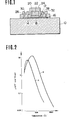
- Fig. 1 shows the preferred embodiment of a MOS thin film transistor which will be referred to hereafter as "MOS TFT".
- MOS TFT MOS thin film transistor
- a thin polycrystalline silicon layer 12 is formed on a quartz substrate 10.
- the polycrystalline silicon layer 12 has n-type regions 14 and 16 at either end, where it is heavily doped with n-type impurities so as to have a relatively low resistance to electron conduction.
- the n-type regions 14 and 16 respectively form a source region and a drain region.
- the central section of the polycrystalline silicon layer defines a channel between the source region 14 and the drain region 16 and serves as an active region 18.
- a gate insulating layer 20 made of silicon dioxide (Si0 2 ) is deposited on the polycrystalline silicon layer 12 so as to cover the active region 18.
- a highly doped polycrystalline silicon (DOPOS) gate electrode 22 is deposited over the gate insulator 20.
- the gate electrode 22 is covered with a silicon dioxide layer acting as an insulator 24.
- the insulator 24 is formed with openings 26 and 28 through which connector electrodes 30 and 32 are formed in contact with the source and drain regions 14 and 16 respectively.
- the gate electrode 22 is also connected to a connector electrode fabricated in a per se well-known manner.
- the thickness t of the polycrystalline layer 12 is adjusted 0 0 to be in the range of 100A to 750A, preferably about 0 200A.
- This preferred thickness range has been derived empirically from experiments performed by the inventor with polycrystalline silicon layers of various thicknesses. The results of these experiments are illustrated in Fig. 2.
- the effective mobility ⁇ eff of the polycrystalline silicon active region increases significantly as the thickness drops o 0 from about 1000A to about 200-500A. As the thickness of the polycrystalline silicon layer drops below 200A, the mobility decreases at a relatively high rate. Also, as shown in Fig. 2, the effective mobility ⁇ eff of the polycrystalline silicon layer is maximized at a thickness of about 200-500A.
- curve A shows the behavior of the effective mobility of a polycrystalline silicon layer which is formed directly into the desired thickness by the process of chemical vapor deposition.
- curve B represents the characteristics of the effective mobility of a polycrystalline silicon layer which is first formed by chemical vapor deposition to a greater than desired thickness and then reduced to its final desired thickness by thermal oxidation.
- a maximum effective mobility of 7.2 cm 2 /V sec was achieved at a thickness of 210A.
- experiments with samples B revealed a maximum effective mobility of 12 cm 2 /V sec at 0 the thickness of 370A.
- the thickness of the polycrystalline silicon active region is chosen to be 200A, and so the effective mobility of an active region of type A will be about 7 cm 2 /V sec and in a circuit employing a layer of type B, about 5 cm 2 /V sec. Therefore, it should be appreciated that the mobility of the polycrystalline silicon layer according to the shown embodiment will be significantly higher than conventional polycrystalline silicon layers. Since the production costs of a polycrystalline silicon layer are much lower than for a single-crystal silicon layer, the overall production cost of MOS TFT's employing the invention can be reduced without sacrificing any of the functional advantages of a single-crystal silicon active region.
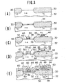
- Figs. 3(A) to 3(E) show a sequence of process steps during fabrication of a C-MOS inverter according to present invention.
- the thin polycrystalline silicon layer is used to good effect in simplifying fabrication of the C- M O S inverter.
- Fig. 3(A) shows the initial stage of fabrication of the C-MOS inverter according to the preferred method of the present invention.
- Field SiO 2 layers 30 are formed on a P-type Si substrate 32 by localized oxidation of silicon (LOCOS). LOCOS is carried out over most of the substrate 32, excluding only the section on which a MOS transistor is to be formed. Thereafter, a layer 36 of polysilicon or amorphous silicon is deposited over the entire surface by chemical vapor deposition.
- LOCOS localized oxidation of silicon
- Si or Ge ion implantation and annealing for 15 hours at a temperature of 600°C may follow deposition of polycrystalline silicon or amorphous silicon in the step shown in Fig.3(B).
- the thickness of the deposited polycrystalline silicon layer falls in the range of 20A to 750A, and preferably in the range of 200A to 400A. Holding the polysilicon layer to the preferred range of thickness ensures that the effective mobility will be adequately high and the leakage current will be acceptably low.
- FIG. 3(B) After performing the process shown in Fig. 3(B), the sections of the polycrystalline silicon layer formed on the field Si0 2 layer, appearing at the edges of Fig. 3(B), are removed, as shown in Fig. 3(C). Gate oxide layers 38 and 39 and gate electrodes 40 and 41 are formed at points on the polycrystalline silicon layer 36 at which an N-channel MOS drive transistor 44 and a P-type MOS load transistor 46 are to be formed.
- N-type ion implantation is performed on the section 48 of the polycrystalline silicon layer 42 on which the N-channel MOS drive transistor 44 is to be formed, as shown in Fig. 3(D).
- the resulting N+ regions to either side of the gate 40 serve as source region 50 and drain region 52 of the NMOS drive transistor 44.
- P-type ion implantation is performed at the site of the P-channel MOS load transistor 46 to form its source region 56 and drain region 58.
- a relatively thick layer 60 of Si0 2 is deposited over the entire surface of the IC for insulation.
- Contact windows are etched through the oxide layer 60 through which a source electrode 62, a drain electrode 64 and a bridging electrode 66 which bridges between the drain region 52 of N-channel MOS drive transistor and the source region 56 of the P-channel MOS load transistor can contact the corresponding doped regions 50, 58, and 52/56, as shown in Fig. 3(E).
- the crystal grains of the vapor-deposited polysilicon layer 36 will tend to grow large enough to minimize the effect of carrier traps along grain boundaries. Furthermore, if an additional annealing step is added following the Si + or Ge ion implantation process, the polysilicon layer may fully recrystallize into a single-crystal silicon layer. In either case, the source region and the drain region formed in the polycrystalline silicon layer will have a sufficiently high effective mobility.
- the fabrication process for a C-MOS inverter can be significantly simplified.
- the polycrystalline silicon layer is deposited onto the areas of the substrate on which the N-channel MOS drive transistor and the P-channel MOS load transistor are to be formed prior to formation of the N-channel MOS drive transistor which is conventionally formed directly on the single-crystal silicon substrate. This allows both of the aforementioned transistors to be formed at the same time in a single step following vapor-deposition of the polycrystalline silicon layer, which has conventionally required at least two separate, independent steps.
- the source regions and drain regions of the N-channel MOS drive transistor and P-channel MOS load transistor are formed in the same polycrystalline silicon layer, connection of the drain region of the N-channel MOS drive transistor to the source region of the P-channel MOS load transistor is greatly facilitated, in that the adjoining drain and source regions can be connected simply by means of the single bridging electrode.
- the gate electrodes for both of the transistors can be formed in a single step and at the same time, connecting the transistors to each other requires only a single phto - lithographic step and so obviates the need for the additional steps needed in fabrication of conventional transistors.
- the source regions and drain regions may extend over wider areas than in conventional devices, the contact windows need not be as finely delineated, which further expedites the fabrication process.
- Figs. 4(A) to 4(E) show essentially the same fabrication process for a C-MOS inverter as shown in Figs. 3 but in this case the step illustrated in Fig. 4(B) includes the Si + or Ge ion implantation and annealling steps mentioned previously. All of the steps other than that shown in Fig. 4(B) are substantially the same as described with reference to Figs. 3(A) to 3(E).
- Si + or Ge + ion implantation is performed following the step of depositing polycrystalline silicon or amorphous silicon on the P-type silicon substrate.
- annealing is performed for 15 hours at a temperature of approximately 600°C. This improves mobility characteristics of the polycrystalline silicon layer significantly.
- the ion implantation and annealing steps increases the average polysilicon grain size in sections where the polysilicon layer is in contact with the single crystal layer to the point where the layer 36 may be traversed by single crystal grains, which makes the properties thereof essentially identical to single-crystal silicon.
- the illustrated embodiment concerns an N-channel MOS transistor on a P-type substrate and a P-channel MOS transistor on a field Sio 2 layer, it would be possible to form a P-channel MOS transistor on an N-type silicon substrate and an N-channel MOS transistor on the field Sio 2 layer.
Landscapes
- Thin Film Transistor (AREA)
- Metal-Oxide And Bipolar Metal-Oxide Semiconductor Integrated Circuits (AREA)
Applications Claiming Priority (4)
| Application Number | Priority Date | Filing Date | Title |
|---|---|---|---|
| JP58251813A JPH0669094B2 (ja) | 1983-12-23 | 1983-12-23 | 電界効果型トランジスタ |
| JP251813/83 | 1983-12-23 | ||
| JP59105192A JPS60249356A (ja) | 1984-05-24 | 1984-05-24 | 半導体装置の製造方法 |
| JP105192/84 | 1984-05-24 |
Publications (3)
| Publication Number | Publication Date |
|---|---|
| EP0152625A2 true EP0152625A2 (fr) | 1985-08-28 |
| EP0152625A3 EP0152625A3 (en) | 1987-07-01 |
| EP0152625B1 EP0152625B1 (fr) | 1992-05-06 |
Family
ID=26445530
Family Applications (1)
| Application Number | Title | Priority Date | Filing Date |
|---|---|---|---|
| EP84116302A Expired - Lifetime EP0152625B1 (fr) | 1983-12-23 | 1984-12-24 | Procédé de la réalisation d'un dispositif à semi-conducteur comportant une région active en silicium. |
Country Status (3)
| Country | Link |
|---|---|
| EP (1) | EP0152625B1 (fr) |
| CA (1) | CA1228935A (fr) |
| DE (1) | DE3485706D1 (fr) |
Cited By (6)
| Publication number | Priority date | Publication date | Assignee | Title |
|---|---|---|---|---|
| EP0222215A3 (en) * | 1985-10-23 | 1988-01-07 | Hitachi, Ltd. | Polysilicon mos transistor and method of manufacturing the same |
| EP0397034A1 (fr) * | 1989-05-09 | 1990-11-14 | Hitachi, Ltd. | Composant SRAM utilisant un film de silicium polycristallin très mince et méthode de fabrication |
| EP0235827B1 (fr) * | 1986-03-06 | 1993-08-11 | Sony Corporation | Tête d'impression à chaleur équipée d'un transistor super mince d'un film de silicone polycristallin |
| EP0562271A1 (fr) * | 1992-03-26 | 1993-09-29 | Texas Instruments Incorporated | Structure haute tension avec source isolée par oxyde et région RESURF de drift dans du silicon massif |
| WO1997008747A1 (fr) * | 1995-08-28 | 1997-03-06 | Siemens Aktiengesellschaft | Procede pour produire une structure semi-conductrice eeprom |
| WO2008012332A1 (fr) * | 2006-07-28 | 2008-01-31 | Austriamicrosystems Ag | Composant avec un transistor à film mince et des transistors cmos, ainsi que procédé pour sa fabrication |
Family Cites Families (1)
| Publication number | Priority date | Publication date | Assignee | Title |
|---|---|---|---|---|
| US4335161A (en) * | 1980-11-03 | 1982-06-15 | Xerox Corporation | Thin film transistors, thin film transistor arrays, and a process for preparing the same |
-
1984
- 1984-12-21 CA CA000470775A patent/CA1228935A/fr not_active Expired
- 1984-12-24 DE DE8484116302T patent/DE3485706D1/de not_active Expired - Lifetime
- 1984-12-24 EP EP84116302A patent/EP0152625B1/fr not_active Expired - Lifetime
Cited By (8)
| Publication number | Priority date | Publication date | Assignee | Title |
|---|---|---|---|---|
| EP0222215A3 (en) * | 1985-10-23 | 1988-01-07 | Hitachi, Ltd. | Polysilicon mos transistor and method of manufacturing the same |
| EP0235827B1 (fr) * | 1986-03-06 | 1993-08-11 | Sony Corporation | Tête d'impression à chaleur équipée d'un transistor super mince d'un film de silicone polycristallin |
| EP0397034A1 (fr) * | 1989-05-09 | 1990-11-14 | Hitachi, Ltd. | Composant SRAM utilisant un film de silicium polycristallin très mince et méthode de fabrication |
| EP0562271A1 (fr) * | 1992-03-26 | 1993-09-29 | Texas Instruments Incorporated | Structure haute tension avec source isolée par oxyde et région RESURF de drift dans du silicon massif |
| WO1997008747A1 (fr) * | 1995-08-28 | 1997-03-06 | Siemens Aktiengesellschaft | Procede pour produire une structure semi-conductrice eeprom |
| US5970338A (en) * | 1995-08-28 | 1999-10-19 | Siemens Aktiengesellschaft | Method of producing an EEPROM semiconductor structure |
| WO2008012332A1 (fr) * | 2006-07-28 | 2008-01-31 | Austriamicrosystems Ag | Composant avec un transistor à film mince et des transistors cmos, ainsi que procédé pour sa fabrication |
| US8008664B2 (en) | 2006-07-28 | 2011-08-30 | austriamicrosystms AG | Component comprising a thin-film transistor and CMOS-transistors and methods for production |
Also Published As
| Publication number | Publication date |
|---|---|
| EP0152625A3 (en) | 1987-07-01 |
| DE3485706D1 (de) | 1992-06-11 |
| EP0152625B1 (fr) | 1992-05-06 |
| CA1228935A (fr) | 1987-11-03 |
| CA1251579C (fr) | 1989-03-21 |
Similar Documents
| Publication | Publication Date | Title |
|---|---|---|
| US5172203A (en) | Semiconductor device with polycrystalline silicon active region and method of fabrication thereof | |
| US4395726A (en) | Semiconductor device of silicon on sapphire structure having FETs with different thickness polycrystalline silicon films | |
| US4373249A (en) | Method of manufacturing a semiconductor integrated circuit device | |
| US4935379A (en) | Semiconductor device and method of manufacturing the same | |
| US6861304B2 (en) | Semiconductor integrated circuit device and method of manufacturing thereof | |
| US4876582A (en) | Crystallized silicon-on-insulator nonvolatile memory device | |
| US4654958A (en) | Process for forming isolated silicon regions and field-effect devices on a silicon substrate | |
| EP0166003A1 (fr) | Circuit integre a semi-conducteurs | |
| EP0119400A1 (fr) | MOSFET de type vertical et procédé pour sa fabrication | |
| US4336550A (en) | CMOS Device with silicided sources and drains and method | |
| JPH039631B2 (fr) | ||
| JPH05102483A (ja) | 薄膜トランジスタ及びその製造方法 | |
| KR870005466A (ko) | 고도로 집적된 회로의 제조공정 | |
| JP3025385B2 (ja) | 半導体装置 | |
| US5300443A (en) | Method for fabricating complementary enhancement and depletion mode field effect transistors on a single substrate | |
| US5242844A (en) | Semiconductor device with polycrystalline silicon active region and method of fabrication thereof | |
| US5264721A (en) | Insulated-gate FET on an SOI-structure | |
| JPS63120442A (ja) | 半導体にドープして接続部に導電性スルーホールを形成する方法 | |
| US6184070B1 (en) | Thin film transistor and method of manufacturing the same | |
| EP0152625B1 (fr) | Procédé de la réalisation d'un dispositif à semi-conducteur comportant une région active en silicium. | |
| GB2064866A (en) | Field effect semiconductor device | |
| JPS61263274A (ja) | 半導体装置の製造方法 | |
| JPS63261880A (ja) | 薄膜トランジスタの製造方法 | |
| CA1251579A (fr) | Dispositif a semiconducteur a region active en silicium polycristallin et methode de fabrication | |
| US4196507A (en) | Method of fabricating MNOS transistors having implanted channels |
Legal Events
| Date | Code | Title | Description |
|---|---|---|---|
| PUAI | Public reference made under article 153(3) epc to a published international application that has entered the european phase |
Free format text: ORIGINAL CODE: 0009012 |
|
| AK | Designated contracting states |
Designated state(s): DE FR GB NL |
|
| PUAL | Search report despatched |
Free format text: ORIGINAL CODE: 0009013 |
|
| AK | Designated contracting states |
Kind code of ref document: A3 Designated state(s): DE FR GB NL |
|
| 17P | Request for examination filed |
Effective date: 19871231 |
|
| 17Q | First examination report despatched |
Effective date: 19900227 |
|
| GRAA | (expected) grant |
Free format text: ORIGINAL CODE: 0009210 |
|
| AK | Designated contracting states |
Kind code of ref document: B1 Designated state(s): DE FR GB NL |
|
| REF | Corresponds to: |
Ref document number: 3485706 Country of ref document: DE Date of ref document: 19920611 |
|
| ET | Fr: translation filed | ||
| PLBE | No opposition filed within time limit |
Free format text: ORIGINAL CODE: 0009261 |
|
| STAA | Information on the status of an ep patent application or granted ep patent |
Free format text: STATUS: NO OPPOSITION FILED WITHIN TIME LIMIT |
|
| 26N | No opposition filed | ||
| REG | Reference to a national code |
Ref country code: GB Ref legal event code: IF02 |
|
| PGFP | Annual fee paid to national office [announced via postgrant information from national office to epo] |
Ref country code: NL Payment date: 20031205 Year of fee payment: 20 |
|
| PGFP | Annual fee paid to national office [announced via postgrant information from national office to epo] |
Ref country code: FR Payment date: 20031210 Year of fee payment: 20 |
|
| PGFP | Annual fee paid to national office [announced via postgrant information from national office to epo] |
Ref country code: GB Payment date: 20031224 Year of fee payment: 20 |
|
| PGFP | Annual fee paid to national office [announced via postgrant information from national office to epo] |
Ref country code: DE Payment date: 20040102 Year of fee payment: 20 |
|
| PG25 | Lapsed in a contracting state [announced via postgrant information from national office to epo] |
Ref country code: GB Free format text: LAPSE BECAUSE OF EXPIRATION OF PROTECTION Effective date: 20041223 |
|
| PG25 | Lapsed in a contracting state [announced via postgrant information from national office to epo] |
Ref country code: NL Free format text: LAPSE BECAUSE OF EXPIRATION OF PROTECTION Effective date: 20041224 |
|
| REG | Reference to a national code |
Ref country code: GB Ref legal event code: PE20 |
|
| NLV7 | Nl: ceased due to reaching the maximum lifetime of a patent |
Effective date: 20041224 |