EP0153165A2 - Einrichtung und Verfahren zur Abtastung von mehreren Trägersignalen - Google Patents
Einrichtung und Verfahren zur Abtastung von mehreren Trägersignalen Download PDFInfo
- Publication number
- EP0153165A2 EP0153165A2 EP85301012A EP85301012A EP0153165A2 EP 0153165 A2 EP0153165 A2 EP 0153165A2 EP 85301012 A EP85301012 A EP 85301012A EP 85301012 A EP85301012 A EP 85301012A EP 0153165 A2 EP0153165 A2 EP 0153165A2
- Authority
- EP
- European Patent Office
- Prior art keywords
- shift register
- output
- frequency
- phase
- pulse
- Prior art date
- Legal status (The legal status is an assumption and is not a legal conclusion. Google has not performed a legal analysis and makes no representation as to the accuracy of the status listed.)
- Granted
Links
Images


Classifications
-
- H—ELECTRICITY
- H04—ELECTRIC COMMUNICATION TECHNIQUE
- H04J—MULTIPLEX COMMUNICATION
- H04J1/00—Frequency-division multiplex systems
- H04J1/02—Details
- H04J1/04—Frequency-transposition arrangements
- H04J1/05—Frequency-transposition arrangements using digital techniques
-
- H—ELECTRICITY
- H04—ELECTRIC COMMUNICATION TECHNIQUE
- H04B—TRANSMISSION
- H04B3/00—Line transmission systems
- H04B3/54—Systems for transmission via power distribution lines
- H04B3/542—Systems for transmission via power distribution lines the information being in digital form
-
- H—ELECTRICITY
- H04—ELECTRIC COMMUNICATION TECHNIQUE
- H04B—TRANSMISSION
- H04B2203/00—Indexing scheme relating to line transmission systems
- H04B2203/54—Aspects of powerline communications not already covered by H04B3/54 and its subgroups
- H04B2203/5462—Systems for power line communications
- H04B2203/5466—Systems for power line communications using three phases conductors
-
- H—ELECTRICITY
- H04—ELECTRIC COMMUNICATION TECHNIQUE
- H04B—TRANSMISSION
- H04B2203/00—Indexing scheme relating to line transmission systems
- H04B2203/54—Aspects of powerline communications not already covered by H04B3/54 and its subgroups
- H04B2203/5462—Systems for power line communications
- H04B2203/5483—Systems for power line communications using coupling circuits
-
- H—ELECTRICITY
- H04—ELECTRIC COMMUNICATION TECHNIQUE
- H04B—TRANSMISSION
- H04B2203/00—Indexing scheme relating to line transmission systems
- H04B2203/54—Aspects of powerline communications not already covered by H04B3/54 and its subgroups
- H04B2203/5462—Systems for power line communications
- H04B2203/5491—Systems for power line communications using filtering and bypassing
-
- H—ELECTRICITY
- H04—ELECTRIC COMMUNICATION TECHNIQUE
- H04B—TRANSMISSION
- H04B2203/00—Indexing scheme relating to line transmission systems
- H04B2203/54—Aspects of powerline communications not already covered by H04B3/54 and its subgroups
- H04B2203/5462—Systems for power line communications
- H04B2203/5495—Systems for power line communications having measurements and testing channel
Definitions
- the present invention relates generally to apparatus for the reception of carrier signals and, more specifically, to apparatus for sampling a plurality of carrier signals at diverse times in order to overcome the potential ambiguity of valid carrier signals during periods of short duration electrical noise which is common to more than one phase of a polyphase electrical transmission system.
- a high frequency carrier signal such as a 12.5 kilohertz carrier signal
- a receiver removes the carrier signal from the 60 hertz current, by passing it through a high pass filter, and then examines the carrier signal in order to extract digital data.
- carrier signal demodulators can be used to extract the digital data from the phase shift keyed carrier.
- the electrical noise normally found on power lines contains components which are periodic and aperiodic, impulsive and continuous.
- Periodic noise of both the impulsive and continuous types usually has a period which is some harmonic of the power frequency, such as 60 hertz, and originates from loads on the power line such as SCR'S, rotating equipment, etc.
- Aperiodic noise is generally impulsive and is the result of random events such as switch closures and electrical lightning.
- Impulsive noise is normally dominant on power lines.
- Most power line carrier signals differ from noise in that they are usually continuous waveforms such as those employed by frequency shift keyed or phased shift keyed modulation and they avoid high energy content at harmonics of the power line frequency.
- the sampling frequencies utilized by the aforementioned demodulation EPC patent publicaitons are specifically selected to minimize the impact of most impulsive noise by separating the samples by multiple carrier cycles.
- a signal is sent from a transmitter which is operatively connected to a single phase electrical system, such as that of a personal residence, and received by a receiver which is located at a remote location and operatively connected to a three phase power line system.
- a carrier signal transmitted on one phase of a polyphase electrical transmission system can be-coupled to one or both of the other two phases.
- the strength of these coupled signals are dependent on many factors, such as the length of transmission line over which the signal is present, the configuration of that power line, the frequency content of the signal along with other power line characteristics. Note that these coupling mechanisms act equally on carrier signals and electrical noise. Under these circumstances, the receiver can receive and monitor signals on any one or all three of the phases available to it.
- a receiver it is preferable for a receiver to be configured in such a way that it is capable of monitoring signals on all three phases of the electrical transmission line.
- U.S. Patent No. 4,382,248 which issued to Pai on May 3, 1983 discloses such a polyphase receiver and should be consulted for a more complete understanding thereof.
- the aforementioned coupling of carrier signals between associated phases of a polyphase power line system can be used advantageously by a receiver.
- the receiver can be connected in such a way that it can monitor signals on all of the phases and these signals can be combined in any one of a number of known techniques in order to result in a single carrier signal which can be decoded to determine its digital message.
- a significant benefit can be achieved by having a receiver monitor all phases of a polyphase power line system.
- the benefits of this type of polyphase reception system can be best realized by comparing it to an alternate system which only monitors one phase.
- the presence of electrical noise on the monitored phase can cause a demodulator to miss a valid carrier signal.
- sophisticated techniques for interpreting carrier signals have been developed and are disclosed in the above-mentioned EPC patent publications, the possibility remains that electrical noise impulses on the transmission line can disturb the demodulation of the carrier signal or extend the time required in order for a demodulator to determine that a valid carrier signal is present.
- the carrier signals received on each of the three phases can be compared and combined in order to enhance the determination of the presence or absence of a signal at any given instance of time. If electrical noise is present on one of the three phases, a combination of that signal with the signals received on the other two phases can be made to diminish the effects of that noise on the demodulation process. Therefore, the concurrent monitoring of all_ phases by a receiver is advantageous when spurious electrical noise exists which is different in content on each of the three phases.
- a second, more common, cause for electrical noise appearing coincidentally on all phases of a power line is that, when electrical noise exists on one phase of a three phase system, that noise is coupled to the other phases in a manner similar to that which couples carrier signals between the phases of a three phase system.
- the degree of coupling between phases is dependent on the same multiplicity of factors that applies to signal coupling.
- the chief object of the present invention is to provide a method and apparatus for sampling a plurality of carrier signals in a three phase receiver to reduce the probability of a signal noise impulse, common to multiple phases, from generating erroneous samples on all of those phases.
- the invention resides in a method for sampling a plurality of carrier signals, comprising: providing a shift register with two outputs, said two outputs being operatively associated with different entries of a data string within said shift register; inputting a clock pulse at a preselected first frequency into said shift register which causes said data string to shift within said shift register; inputting a sample pulse at a preselected second frequency into said shift register, said sample pulse being entered into said data string, said first frequency being higher than said second frequency, said first and second frequencies being related by an integer multiple, said sample pulse being synchronized with said clock pulse; operatively connecting a first one of said two outputs to a first means for determining an instantaneous logic level of a first carrier signal; and operatively connecting a second of said two outputs to a second means for determining an instantaneous logic level of a second carrier signal.
- the invention further resides in apparatus for sampling a plurality of carrier signals, operating according to the above method comprising: first means for providing a sample pulse, said sample pulse having a first frequency; second means for providing a clock pulse, said clock pulse having a second frequency; means for causing a first output signal a first predetermined time period after an occurrence of said sample pulse, said first predetermined time period being generally equal to a first integral member of occurrences of said clock pulses; said means for causing a first output signal also causing a second output signal a second predetermined time period after an occurrence of said sample pulse, said second predetermined time period being generally equal to a second integral number of occurrences of said clock pulse; first means for measuring the instantaneous logic level of a carrier signal, said first measuring means being cooperatively associated with said causing means, said first measuring means being responsive to said first output signal; second means for measuring the instantaneous logic level of a carrier signal, said second measuring means also being cooperatively associated with said causing means, said second measuring means being responsive to said second
- the present disclosure reveals a method and apparatus to sample all phases of a three phase system in a manner which minimizes the probability that multiple erroneous samples will occur due to a single noise impulse existing simultaneously.
- Sampling on a time diversity basis increases the probability of at least one phase of a three phase receiver having a signal-to-noise ratio much greater than the remaining two phases. This is accom - plished by providing a preselected time delay between the sampling of the phases. While providing time diversity between samples on the different phases, the present invention maintains a consistency of timing between sequential samples taken on any specific phase.
- a device such as a shift register, which is capable of shifting a string of digital data.
- a shift register enables the present invention to maintain a pattern of bits which is sequentially shifted as a function of time. As the data is shifted through the shift register, preselected outputs of the register are used to activate sampling mechanisms which are cooperatively associated with each of the phases.
- a periodic sample pulse is used as a data input to the shift register in order to change the logic level of the data being shifted through the register.
- a periodic clock pulse is used to cause the actual shifting of the data.
- the clock pulse frequency must be higher than the sample pulse frequency.
- the clock pulse frequency is chosen to be an integer multiple of the sample pulse frequency and each occurrence of a sample pulse is coincident with an occurrence of a clock pulse to provide synchronization between the clock pulse and sample pulse frequencies.
- the sample pulse proceeds through the data string of the shift register, different outputs of the shift register are affected by any given data bit at different times. Therefore, as the sample pulse proceeds to the first preselected output of the shift register, its logic level will be transmitted to the first phase sampling means. Sequentially, as that same sample pulse is shifted through the shift register, it eventually reaches a second output and the logic level of the sample pulse will activate a second phase sampling means in much the same way as it previously affected the first phase sampling means. By determining the frequency of both the sample and clock pulses, the frequency of sampling for each phase can be determined. Furthermore, the choice of outputs of the shift register will determine the time delay between the sampling of the phases.
- the primary function of any power line communication system is to transmit information between a central utility location and a customer location, over the primary and secondary distribution conductors of a power line.
- information can consist of metering data, load status information or various other useful data in automated distribution systems
- the basic operation of such a system requires the data to be converted at a transmitter to strings of binary data bits in a predetermined message format.
- baseband data is the sequential string of "ones" and "zeros" which are arranged according to a particular protocol in order to represent a message.
- the baseband data is modulated onto a carrier signal by causing the phase of the carrier to assume predetermined phases according to the logic state of the baseband data bits.
- the modulated carrier signal is then coupled to the power line conductor and propagated to the destination where a receiver is located.
- the carrier signal is of a much higher frequency than the 60 hertz current of the power line. This carrier frequency is typically between 5 kHz and 15 kHz.
- Figure 1 illustrates a time based graph of the logic states of the signals of binary baseband data 10 the beginning portion of a carrier data transmission message would typically include a preamble, illustrated in Figure 1 between times TO and T2, which comprises a series of sequential "zeros" and "ones", or lows and highs, and ending with two consecutive "ones".
- the preamble consists of a preselected number of alternating "ones" and zeros" and the two consecutive "ones" at the end of the preamble identify the preamble's end and the message's beginning for the receiver.
- each logic level change of the baseband data 10 illustrated in Figure 1 actually represents many individual pulses of a carrier signal.
- the reasons for using many carrier pulses to represent a single logic level of a baseband data string will be described below.
- Figure 2 illustrates an expanded version of the baseband data which is shown in Figure 1. Comparing Figures 1 and 2, it can be seen that the portion of the baseband data which represents the first "zero" or low level segment of the baseband data in Figure 1, between times TO and Tl, actually comprises a plurality of individual carrier signal pulses.
- the time period between TO and Tl is functionally divided into four individual carrier segments.
- the first carrier segment would extend between times TO and TO-I
- the second carrier segment would extend between times TO-1 and TO-2, and so on.
- Each carrier segment comprises 41 cycles of a carrier signal.
- the carrier signal in Figure 2 is broken for purposes of illustration, it should be understood that between times TO and Tl, 164 cycles of a carrier signal are used to formulate the four carrier segments which make up a single data bit of the baseband data 10.
- Each carrier segment consists of 41 carrier signal cycles 20.
- FIG 3 illustrates an expanded view of one carrier segment.
- This carrier segment which occurs between time TO and TO-1 would comprise one fourth of the total number of carrier signal cycles that exist in one baseband data bit.
- one baseband data bit is illustrated in Figures 1 and 2 as occurring between times TO and T1.
- carrier signal cycles 20 combined to form the illustrated carrier segment.
- the carrier segment can be periodically sampled and the logic level of the carrier signal can be stored.
- the plurality of samples for a given carrier segment can then be algorithmically manipulated in order to determine the relative position in time of its high and low logic levels. This enables a demodulator to determine the phase characteristics of each carrier segment and, therefore, the phase characteristics of the related baseband data bit which comprises four such carrier segments.
- the carrier signal originates as a sinusoidal waveform and remains sinusoidal during transmission over the electrical power lines.
- the sinusoidal waveform is hard limited and this procedure results in a square wave carrier signal.
- FIGs 4A and 4B illustrate the relationship between a sinusoidal carrier signal and its corresponding square wave resulting from the hard limiting procedure.
- the sinusoidal carrier signal 40 is shown. It should be understood that the sinusoidal carrier 40 would typically be a high frequency signal, of between 5 kHz and 15 kHz, which is imposed on a lower frequency current, such as the 50 or 60 hertz frequency in typical power line systems.
- the waveform illustrated in Figure 4A represents the carrier signal 40 as it would appear after passing through a high pass filter that would remove the lower frequencies, such as the 60 hertz waveform.
- phase shift keyed carrier signals logic level changes are represented by phase shifts such as the shift which is illustrated by reference numeral 42.
- the phase shift 42 would represent a change of state from a logic level 0 to a logic level 1, or vice versa.
- the sinusoidal waveform 40 would be hard limited. Hard limiting would transform the sinusoidal waveform 40 into a square wave configuration 44 as illustrated in Figure 4B. The hard limiting of the phase shift 42 of Figure 4A would result in the square wave portion 46 in Figure 4B. In this particular example, the phase shift 42 resulted in two sequential logic level "ones" following the hard limiting operation. It should also be understood that had the phase shift of the sinusoidal wave occur 180° later than illustrated in Figure 4A, the resulting square wave carrier signal would have two sequential logic level "zeros". Throughout this discussion, a convention will be used in which a high logic level signal will represent a binary digit one and a low level signal will represent a binary digit zero.
- Figures 4A and 4B therefore illustrate the means by which a coherent phase shift keyed demodulation technique can transmit binary data from a transmitter to a remote receiver.
- the valid signal is highly cyclic with a period specifically selected to differ from any expected noise frequency. Receiver signal sampling patterns are chosen to accent these differences and to reduce the impact of the occurrence of electrical noise in the samples.
- the impact of noise on demodulation operation is a direct function of the correlation of noise with the sampling pattern.
- Each of the received signal samples is independently correlated with an expected carrier waveform and then these correlations are combined by the demodulator with earlier sample correlations for signal determination. When a valid signal is sampled, these sample correlations are additive as would be indicative of a valid signal.
- Correlations of noise samples tend to be more random and, therefore, cancel each other in a manner which is indicative of the absence of a valid signal.
- each of the three samples is still independently correlated.
- reception is enhanced since the number of additive correlation elements is increased.
- Noise on multiple phases, where the noise on each phase is independent still cancels even when all three phases are sampled at the same time because of differences in their correlations.
- Noise on multiple phases, where the noise is common to more than one phase is additive where all phases are sampled at the same time, thus increasing the demodulator sensitivity to this type of noise. Since the effects of phase-to-phase coupling are identical for signal and noise based on energy and frequency content, significant amounts of coupled noise is found.
- Figure 5 is a time based illustration of a hypothetical transmitted carrier signal 50 and the representation of that carrier signal as it would appear on the three phases of a transmission power line as the signals are received by a receiver.
- Carrier signals 51, 52 and 53 would arrive at the receiver's location on phases A, B and C, respectively. It should be understood that, in Figure 5, the carrier signals are represented as square waves in order to illustrate their appearance following a hard limiting procedure. As discussed above, these carrier signals, 51-53, would travel along the power lines as sinusoidal waveforms prior to their being hard limited at the receiver's location.
- carrier signal 50 represents the valid noise-free carrier signal as originally transmitted.
- the hard limited noise pulses 56 are cross hatched for illustration purposes in Figure 5.
- phase A would indicate a logical low level or a binary digit "zero".
- phase C would indicate a logical high level.
- the three values taken at time Sl could be compared in such a way so as to deduce that a noise pulse must have caused the logical high level sensed on phase C.
- phases B and C would indicate a logical low level while phase A would indicate a logical high level.
- the results of this sample could be algorithmically determined to be a logical low level, with a noise pulse existing on phase A.
- FIG. 6 illustrates a functional diagram of three phase samplers, 61, 62 and 63.
- Conductive lines, 64, 66 and 68 are cooperatively associated with the phase samplers.
- the conductive lines each have a square wave carrier signal passing through them.
- the three conductive lines, 64, 66 and 68, are associated with the phase samplers, 61, 62 and 63, in such a way that the voltage level of the square wave carrier signal on each of the conductive lines can be instantaneously sampled.
- a data shifting means 70 which has the capability of storing and shifting 128 binary digits, is illustrating in Figure 6 with three preselected outputs connected to the three phase samplers, 61, 62 and 63. As shown in Figure 6, an output from the 16th, 32nd and 48th data string positions are operatively connected to the phase samplers, 61, 62 and 63, respectively.
- phase sampler 61 which is associated with phase 1.
- phase samplers 62 and 63 are activated, respectively.
- each sequential pulsing of the shifting means 70 by an appropriate clock pulse would cause that binary digit 1 to move to the right into sequential positions of the shifting means 70.
- a signal would be sensed by the phase sampler 61 for the first phase and the instantaneous voltage level of the carrier signal on the conductive line 64 would be recorded and stored.
- the timed diversity between samples on any two phases can easily be determined if the associated output locations of the shifting means 70 for those phases is known and the frequency of the clock pulse is known.
- the sample diversity between any two phases then is the product of the number of stages of the shifting means between sample controls for those phases in the period of the clock pulse train. By way of example, if this product is equal to an integer times the period of the carrier signal, then the samples of valid carrier signals within the same baud interval.will have identical values for the different phases in the absence of noise. Note that this condition allows the demodulator to act on the samples as if they occurred at the same time for each phase while assuring the time diversity which decreases the probability of common noise samples from multiple phases.
- the frequency at which a new binary digit 1 is inserted into the first location of the shifting means 70 determines the frequency at which any specific phase is sampled. As an example, if a sample pulse FS is caused to occur every 410 microseconds and a clock pulse is caused to occur every 10 microseconds, each phase will be sampled at the rate of once every 410 microseconds. Furthermore, by knowing that phases 1 and 2 are operatively associated with locations 16 and 32 of the shifting means, respectively, it can be easily determined that phase 2 will be sampled 160 microseconds after phase 1 is sampled. Also, since phase 2 and phase 3 are operatively connected to outputs of the shifting means 70 which are 16 locations apart, phase 3 will be sampled 160 microseconds after phase 2 is sampled.
- phase two will be sampled 160 microseconds after phase one is sampled and phase three will be sampled 160 microseconds after phase two is sampled.
- phase one will again be sampled 90 microseconds after phase three is sampled.
- the shifting means 70 are rows and columns of binary digits which represent the contents of the illustrated locations of the shifting means 70 at various points in time.
- the points in time, TO-T 48 have been numbered coincidentally with associated pulses of a clock which has a 10 microsecond period.
- all locations of the shifting means 70 are shown as having binary digit zeros in them.
- a binary digit 1 is placed in the first location of the shifting means 70 by an appropriate means for supplying a sample pulse F S .
- the binary digit 1 is shifted into the second location of the shifting means 70.
- the binary digit 1 can be seen in the third location of the shifting means 70. This process would continue as sequential clock pulses cause the binary data to shift through the shifting means 70 and at time T 15 the binary digit would be located in the 15 location of the shifting means 70.
- phase sampler 61 When the binary digit 1 is shifted into the 16 location of the shifting means 70, at time T 16 , a signal is sent to the phase sampler 61 for phase 1 and the phase sampler 61 records and stores the instantaneous logical level of its associated carrier signal.
- the clock pulses would continue and, at time T 32 , the binary digit would be shifted into location 32, causing the phase sampler 62 which is operatively associated with phase 2 to record and store the instantaneous logical level of its associated carrier signal.
- This process would continue and, at time T 48' the binary digit would be shifted into location 48 of the shifting means 70 and the instantaneous logical level of the carrier signal associated with phase 3 would be sampled and stored.
- phase samplers associated with the three phases of the transmission system can be sequentially activated at predetermined time diversity intervals.
- the pulse at the output of the shifting means 70 would still be only a single pulse, but it would be longer in duration than a single clock pulse and would be, in fact, equivalent in duration to an integer number of clock pulses. In most applications, this circumstance presents no problem since the phase samplers, 61-63, can be chosen to be activated by the leading edge of a change of logic level state. Therefore, when the contents of a specific location of the shifting means 70 changes from a 0 state to a 1 state, its associated phase sampler would be activated, but upon the shifting of another binary digit one into that location, no activation would occur.
- the shifting means 70 would actually have clusters of ones passing through it and each cluster would be separated by a significant series of "zeros".
- the leading binary digit one of each cluster would be the operative digit in activating each of the phase samplers.
- the conductive lines, 64, 66 and 68 are not the electrical transmission lines discussed above. Instead, they are means of transmitting the square wave carrier signals after the sinusoidal carrier signal is passed through a high pass filter and is hard limited.
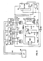
- FIG. 7 illustrates a schematic diagram of a preferred embodiment of the present invention.
- a shifting means 70 is provided which has three outputs, 71, 72 and 73, which are each associated with different locations of its data string. In the example shown in Figure 7, the three outputs, 71, 72 and 73, are associated with locations 16, 32 and 48, respectively, of the shifting means 70. Also illustrated is a source of sample pulses F Sample connected as an input to the shifting means 70. A source of clock pulses FClock are connected as another input to the shifting means 70. Upon each occurrence of a sample pulse, a binary digit "one" is inserted into the first location of the shifting means 70 and upon each occurrence of a clock pulse, the data string within the shifting means 70 is shifted one location.
- each of the phase samplers determines and stores the instantaneous magnitude of the voltage level of the carrier signal on its associated phase.
- the phase samplers are not illustrated as being electrically connected to the conductive lines used in Figure 6. However, it should be understood that each of the phase samplers would be operatively associated with a corresponding carrier signal transmission device.
- NAND gate 74 has three inputs and a single output. One of the inputs of the NAND gate 74 is connected to the third of the three outputs from the shifting means 70. A second input of the NAND gate 74 is connected to the source of clock pulses. The output of the NAND gate 74 is connected to a
- CLOCK input of the FLIP-FLOP 76 and the Q output of the FLI.P-FLOP 76 is connected as the third input of the NAND gate 74.
- the output of the NAND gate 74 is also connected to the phase samplers, 61-63 through the inverter 79.
- the purpose for this connection is to enable the NAND gate 74 to strobe the phase samplers in such a way so as to latch the most recently sampled results of their respective carrier signal voltage levels. This procedure will be described in greater detail below in conjunction with Figure 8.
- Inverters 78 and 79 are utilized in Figure 7 for the purpose of inverting the logic level of their associated signals in order to more appropriately suit the input requirements of the shifting means 70 and the phase samplers, respectively.
- a microprocessor 80 which uses the outputs of the phase samplers as its inputs.
- the function of the microprocessor 80 is to perform the algorithmic manipulations of the resulting data received from the phase samplers, 61-63.
- the microprocessor 80 is illustrated in Figure 7, it should be understood that it is not part of the present invention and its operations occur subsequent to the functions of the present invention.
- a schematic electrical diagram of the present invention is shown in Figure 8.
- a shift register 170 is shown having three outputs connected to locations 16, 32 and 48 of its data string.
- a preferred embodiment of the present invention would utilize a shift register 170 such as type number MC14562B which is a 128 bit static shift register constructed with MOS P-channel and N-channel enhancement mode devices in a single monolithic structure.
- MC14562B is a 128 bit static shift register constructed with MOS P-channel and N-channel enhancement mode devices in a single monolithic structure.
- data is clocked in and out of the shift register on the positive edge of the clock input. Data outputs are available every 16 bits, from bit 16 through bit 128.
- This type of complementary MOS shift register is primarily used where low powered dissipation or high noise immunity is desired.
- the shift register 170 is analogous in function to the shifting means 70 illustrated in Figures 6 and 7 and discussed above.
- the output from the shift register 170, which is associated with bit 48, is connected to
- a preferred embodiment of the present invention would utilize a NAND gate 174 such as type MM74HC11J available from the National Semiconductor Corporation.
- This type of NAND gate 174 is a low power complementary MOS silicon gate which actually comprises three NAND gates.
- the NAND gate 174 in Figure 8 could be configured by using pins 3, 4 and 5 as its inputs and pin 6 as its output.
- Another input of the NAND gate 174 is a Q output from the FLIP-FLOP 176.
- the FLIP-FLOP 176 would be type SN54LS74 which is available from the Texas Instrument Corporation.
- This type of device is a monolithic, dual, D-type, edge-triggered FLIP-FLOP featuring direct clear and preset inputs and complementary Q and 0 outputs. Input information is transferred to the Q output on the positive edge of the clock pulse. Clock triggering occurs at a voltage level of the clock pulse and is not directly related to the transition time of the positive going pulse. After the clock input threshold voltage has been passed, the data input D is locked out.
- the reset input of the FLIP-FLOP 176 is connected to the output from the shift register 170 which is associated with bit position 48.
- a five volt DC source is connected to both the supply voltage and data input ports of the FLIP-FLOP 176.
- FLIP-FLOP 176 is analogous to FLIP-FLOP 76 which is illustrated in Figure 7 and discussed above.
- the inverters 178 and 179 are utilized to invert the logical signals for purposes of matching the input characteristics of their associated devices.
- a preferred embodiment of the present invention would utilize a hex inverter type MM74HC04J which is available from the National Semiconductor Corporation. This type of device has inputs which are compatible with standard complementary MOS outputs and consists of six three stage inverters.
- a timer 190 is provided as a means for providing the clock pulse F Clock and the sample pulse F Sample .
- a preferred embodiment of the present invention would incorporate a timer such as type MC6840 which is available from the Motorola Corporation.
- This type of programmable timer module is a programmable subsystem component of the M6800 family designed to provide variable system time intervals. It has three 16 bit binary counters, three corresponding control registers and a status register. The counters may be used to cause system interrupts or generate output signals.
- This type of timer may also be utilized for such tasks as frequency measurements, event counting or interval measuring.
- the timer 190 has its two inputs, 02 and 03, connected to the inverter 178 and the shift register 170, respectively. When a timer as described above is used, the 02 and 03 outputs are located at its pins 3 and 6, respectively.
- the CS1 input of the timer 190 is connected to a positive five volt DC source and a resistor Rl.
- the other terminal of the resistor Rl is connected to the PBO terminal of a peripheral interface adapter (PIA) 192.
- PIA peripheral interface adapter
- a peripheral interface adapter 192 such as type MC6821 would be used.
- This type of PIA is available from the Motorola Corporation and provides the universal means of interfacing peripheral equipment to the M6800 microprocessing unit. This type of device is capable of interfacing the microprocessing unit to peripherals through two eight-bit bi-directional peripheral data buses and four control lines. No external logic is required for interfacing to most peripheral devices.
- the terminal of resistor R1 which is connected to the peripheral interface adapter 192 is also connected to ground through a removable jumper 194.
- the removable jumper 194 provides the capability of choosing two alternate frequencies for the clock and sample pulses. These frequencies would be chosen as a function of the particular carrier signal frequency utilized with the present invention. With the removable jumper 194 in place, the timer 190 would output a frequency suitable for use with a carrier signal of 12.5 kilohertz and, with the removable jumper 194 removed, the timer 190 is suitable for use with a carrier signal frequency of 9.615 kilohertz.
- the shift register 170 is connected to a 5 volts DC source and to ground through a capacitor Cl.
- the three outputs of the shift register 170 are each connected to an eight bit shift register.
- These shift registers, 196, 197 and 198 are operatively associated with the outputs of the shift register which are connected to bit locations, 16, 32 and 48, respectively.
- the shift registers, 196, 197 and 198 along with their associated hardware, are analogous to the phase samplers 60, 61, 62 and 63 which are illustrated in Figures 6 and 7 and discussed above.
- Shift registers 196, 197 and 198 are identical and, in a preferred embodiment of the present invention, are type CD4094B or type MC14094B which is available from the Motorola Corporation.
- This type of shift register combines an eight stage shift register with a data latch for each stage and a three state output from each latch. The data is shifted on the positive clock transition and is shifted from the seventh stage to two serial outputs. Data from each stage of the shift register is latched on the negative transition of the strobe input. Data propagates through the latch while the strobe is high. Outputs of the eight data latches in the eight stages of each shift register 196, 197, 198 are controlled by three state buffers which are placed in the high impedance state by a logic low on output enable. As can be seen in Figure 8, each of the eight bit shift registers, 196, 197 and 198, has its clock input connected to an associated output from the shift register 170.
- each shift register Upon an occurrence of a signal at its clock input, each shift register would store the instantaneous voltage level of its associated carrier signal.
- the data input for each of the eight bit shift registers is operatively connected to a conductor on which the associated square wave carrier signal is available. Each of these conductors is connected to ground through a resistor.
- the data inputs for shift registers, 196, 197 and 198 are operatively connected to resistors R2, R3 and R4, respectively.
- shift register 170 which is associated with bit 48 is connected as an input to the NAND gate 174.
- the output of the NAND gate 174 changes state and, after passing through inverter 179, provides a strobe pulse for each of the eight bit shift registers.
- This strobe pulse latches the most recently recorded results of each of the eight bit shift registers, 196, 197 and 198. When eight such results are latched in the eight bit shift registers, the data is transmitted to the microprocessor 180 along the data bus 199.
- the eight bits of data from each of the eight-bit shift registers is transferred to the microprocessor 180, in parallel, along the data bus 199 and the data can then be subsequently examined and manipulated in order to determine the characteristics of each of the three carrier signals, one from each phase.
- microprocessor 180 performs its function after the present invention completes its operation.
- the microprocessor 180 must have the capability to mathematically manipulate its data inputs from the eight bit shift register and perform the necessary algorithms to characterize the phase relationships of the three related carrier signals. Any microprocessor which has the proper I/O and speed capabilities to perform these tasks can be utilized in conjunction with the present invention.
- a preferred embodiment of the present invention utilizes a shift register 170 with three outputs, each of the outputs being associated with a particular bit position of a data string.
- a sample pulse F Sample is provided as an input for the shift register from a timer 190.
- the shift register 170 is also provided with a clock input F Clock from the timer 190.
- the clock pulses have a higher frequency than the sample pulses and the frequencies of these two pulses are related by an integer multiple.
- the timer 190 must be capable of synchronizing each sample pulse with one of the clock pulses.
- the FLIP-FLOP 176 and NAND gate 174 in conjunction with the shift register 170, provide a strobe pulse for the three eight bit shift registers that store the instantaneous values of the carrier signals.
- the resulting data is stored in each of the eight-bit shift registers until the registers are full and, at that time, the data is transferred to a microprocessor 180 for subsequent analysis.
- a microprocessor 180 for subsequent analysis.
- the timing chart of Figure 9 will be used to sequentially describe the process of time diversity sampling which is made possible by the present invention.
- the sequential signals associated with the present invention are plotted along a time line which extends from 0 to.820 microseconds.
- the clock pulses F Clock continuously occur at a frequency of 100 kilohertz, or one pulse every 10 microseconds.
- the clock pulse line is shown broken in the illustration of Figure 9, it should be understood that this was done for convenience and that the clock pulses are continuous throughout the operation of the present invention.
- the sample pulse FSample occurs every 410 microseconds as shown.
- each sample pulse from the Q3 output of timer 190 would change the status of the first bit position of the shift register 170.
- one sample pulse is shown beginning at time zero and extending for approximately 20 microseconds and, after a delay period, another sample pulse begins at time 410 and lasts for approximately 20 microseconds.
- Sixteen clock pulses after. the first sample pulse, or at 160 microseconds, the sample pulse data will have been shifted to the 16th bit position of the data string in the shift register 170. Therefore, as indicated by the line "sample phase one", bit 16 of the shift register 170 will remain at a logical high level until the number of binary digit "ones" deposited by the sample pulse pass through it.
- phase one sample pulse at 160 microseconds, will cause the associated sampling hardware for phase one (reference numeral 61 in Figure 7 or reference numeral 196 in Figure 8) to be activated and a sample of the phase one carrier signal will be stored by the eight-bit shift register 196 which is operatively connected to the bit 16 output of the shift register 170.
- the bottom waveform in Figure 9 represents the phase one carrier signal square wave.
- the "sample” arrow indicates the value which would be shifted in the eight-bit shift register 196. 160 microseconds following the sampling of phase one, or at 320 microseconds, phase two would be sampled because of the passage of the originally described sample pulse into bit 32 of the shift register 170.
- phase two carrier signal is illustrated in Figure 9, it should be understood that a sample value would be taken and stored in the eight-bit shift register 197 which is associated with bit 32 of the shift register 170 and phase two.
- the phase three shift register 198 is activated and the instantaneous logical level of its associated phase three carrier signal is taken and stored in a similar manner to that described above in conjunction with phases one and two.
- the present invention has been configured in such a way so as to sample each phase every 410 microseconds and to sample each of the three phases 160 microseconds apart.
- the choice of 160 microseconds as the interval between phase sampling is not a precise requirement of the present invention. Rather, it is a convenient time interval which spreads the three phase samplings roughly equally throughout the available time frame.
- the availability of a shift register 170 with outputs every 16 bits made this timing selection desirable. It should be understood that the choice of 160 microseconds between the samples of phase one and two and the samples of phase two and three result in a subsequent sampling of phase one 90 microseconds following the sampling of phase three.
- Figure 9 also illustrates the occurrence of a strobe pulse at 70 and 480 microseconds.
- This strobe pulse is coincident with the beginning of the sample pulse for phase 3. This is a result of the three inputs of the NAND gate 174 being satisfied to cause an output, through inverter 179, to the eight-bit shift registers.
- the phase one carrier signal which is shown at the bottom portion of Figure 9, has a frequency of 12.5 kilohertz and a period of 80 microseconds as shown. With this frequency of carrier signal, the choice of a 10 microsecond period for the clock pulse F Clock and a 410 microsecond period for the sample pulse F Sample results in eight samples being accomplished for every 41 pulses of the carrier signal. This results in a sample being taken every 5-1/8 carrier pulses.
- the frequency of the clock pulses F Clock and the sample pulses F Sample are an integer multiple of each other with the clock pulse being a higher frequency than the sample pulse. For example, with a period of 410 microseconds, the sample pulse frequency is 41 times slower than the clock pulse frequency.
- Another important characteristic of the present invention is that each sample pulse occurs simultaneously with a clock pulse. This is an important requirement in order to synchronize the shifting of the data through the shift register with the deposition of the data into the first bit of the shift register.
Landscapes
- Engineering & Computer Science (AREA)
- Computer Networks & Wireless Communication (AREA)
- Signal Processing (AREA)
- Power Engineering (AREA)
- Physics & Mathematics (AREA)
- Electromagnetism (AREA)
- Digital Transmission Methods That Use Modulated Carrier Waves (AREA)
- Synchronisation In Digital Transmission Systems (AREA)
- Cable Transmission Systems, Equalization Of Radio And Reduction Of Echo (AREA)
Applications Claiming Priority (2)
| Application Number | Priority Date | Filing Date | Title |
|---|---|---|---|
| US06/580,504 US4573170A (en) | 1984-02-15 | 1984-02-15 | Apparatus and method for sampling multiple carrier signals |
| US580504 | 2000-05-25 |
Publications (3)
| Publication Number | Publication Date |
|---|---|
| EP0153165A2 true EP0153165A2 (de) | 1985-08-28 |
| EP0153165A3 EP0153165A3 (en) | 1986-09-03 |
| EP0153165B1 EP0153165B1 (de) | 1990-12-12 |
Family
ID=24321365
Family Applications (1)
| Application Number | Title | Priority Date | Filing Date |
|---|---|---|---|
| EP85301012A Expired - Lifetime EP0153165B1 (de) | 1984-02-15 | 1985-02-15 | Einrichtung und Verfahren zur Abtastung von mehreren Trägersignalen |
Country Status (8)
| Country | Link |
|---|---|
| US (1) | US4573170A (de) |
| EP (1) | EP0153165B1 (de) |
| JP (1) | JPS6110333A (de) |
| KR (1) | KR850006803A (de) |
| AU (1) | AU581204B2 (de) |
| CA (1) | CA1220824A (de) |
| DE (1) | DE3580855D1 (de) |
| ZA (1) | ZA85743B (de) |
Cited By (2)
| Publication number | Priority date | Publication date | Assignee | Title |
|---|---|---|---|---|
| EP0604678A1 (de) * | 1992-12-28 | 1994-07-06 | Landis & Gyr Technology Innovation AG | Verfahren zum Betrieb eines Empfängers, der mit Informationen gespeist wird, die über ein elektrisches Energieversorgungsnetz übertragen werden, und Anordnung zur Durchführung des Verfahrens |
| WO1999000393A1 (en) * | 1997-06-26 | 1999-01-07 | Dong Wha Pharmaceutical Industrial Co., Ltd. | Quinolone carboxylic acid derivatives |
Families Citing this family (8)
| Publication number | Priority date | Publication date | Assignee | Title |
|---|---|---|---|---|
| US4766414A (en) * | 1986-06-17 | 1988-08-23 | Westinghouse Electric Corp. | Power line communication interference preventing circuit |
| US5228062A (en) * | 1990-04-16 | 1993-07-13 | Telebit Corporation | Method and apparatus for correcting for clock and carrier frequency offset, and phase jitter in multicarrier modems |
| EP0748480A1 (de) * | 1992-06-30 | 1996-12-18 | Electronic Innovators, Inc. | Verteiltes intelligenzverwaltungssystem zur übertragung von technischen unfall- und schadendaten unter verwendung von einem leistungsträgerstrom-lan |
| GB9605719D0 (en) * | 1996-03-19 | 1996-05-22 | Philips Electronics Nv | Integrated receiver |
| US7590175B2 (en) | 2003-05-20 | 2009-09-15 | Rambus Inc. | DFE margin test methods and circuits that decouple sample and feedback timing |
| US7627029B2 (en) | 2003-05-20 | 2009-12-01 | Rambus Inc. | Margin test methods and circuits |
| US8265197B2 (en) * | 2009-08-03 | 2012-09-11 | Texas Instruments Incorporated | OFDM transmission methods in three phase modes |
| DE102010039716B4 (de) * | 2010-08-24 | 2012-09-20 | Gcd Hard- & Software Gmbh | Verfahren zur Übertragung eines Nutzsignals |
Family Cites Families (13)
| Publication number | Priority date | Publication date | Assignee | Title |
|---|---|---|---|---|
| US438248A (en) * | 1890-10-14 | stewart | ||
| US3271742A (en) * | 1963-11-06 | 1966-09-06 | Ibm | Demodulation system |
| US3575610A (en) * | 1967-09-20 | 1971-04-20 | Nippon Electric Co | Scanning pulse generator |
| US3697881A (en) * | 1969-07-10 | 1972-10-10 | Kokusai Denshin Denwa Co Ltd | Phase detection system for at least one digital phase-modulated wave |
| US3571712A (en) * | 1969-07-30 | 1971-03-23 | Ibm | Digital fsk/psk detector |
| GB1480907A (en) * | 1973-08-10 | 1977-07-27 | Ericsson Telefon Ab L M | Data analysis device for a transit exchange |
| DE2357655B2 (de) * | 1973-11-19 | 1975-09-11 | Siemens Ag, 1000 Berlin Und 8000 Muenchen | Schaltungsanordnung zur Demodulation eines frequenzdifferenziellen phasenmodulierten Signalgemisches |
| US3938052A (en) * | 1974-05-09 | 1976-02-10 | Teletype Corporation | Digital demodulator for phase-modulated waveforms |
| JPS5211806A (en) * | 1975-07-18 | 1977-01-29 | Kokusai Denshin Denwa Co Ltd <Kdd> | Teleprinter code control system |
| US4298984A (en) * | 1976-10-06 | 1981-11-03 | Her Majesty The Queen In Right Of Canada, As Represented By The Minister Of National Defence | Method and apparatus for improving error rate on radio teletype circuits |
| US4311964A (en) * | 1979-09-21 | 1982-01-19 | Westinghouse Electric Corp. | Coherent phase shift keyed demodulator for power line communication systems |
| US4382248A (en) * | 1981-04-09 | 1983-05-03 | Westinghouse Electric Corp. | Remote device for a multi-phase power distribution network communication system |
| US4418333A (en) * | 1981-06-08 | 1983-11-29 | Pittway Corporation | Appliance control system |
-
1984
- 1984-02-15 US US06/580,504 patent/US4573170A/en not_active Expired - Fee Related
-
1985
- 1985-01-30 ZA ZA85743A patent/ZA85743B/xx unknown
- 1985-02-08 AU AU38563/85A patent/AU581204B2/en not_active Ceased
- 1985-02-13 CA CA000474233A patent/CA1220824A/en not_active Expired
- 1985-02-14 JP JP60028136A patent/JPS6110333A/ja active Pending
- 1985-02-15 DE DE8585301012T patent/DE3580855D1/de not_active Expired - Lifetime
- 1985-02-15 KR KR1019850001013A patent/KR850006803A/ko not_active Ceased
- 1985-02-15 EP EP85301012A patent/EP0153165B1/de not_active Expired - Lifetime
Cited By (4)
| Publication number | Priority date | Publication date | Assignee | Title |
|---|---|---|---|---|
| EP0604678A1 (de) * | 1992-12-28 | 1994-07-06 | Landis & Gyr Technology Innovation AG | Verfahren zum Betrieb eines Empfängers, der mit Informationen gespeist wird, die über ein elektrisches Energieversorgungsnetz übertragen werden, und Anordnung zur Durchführung des Verfahrens |
| WO1999000393A1 (en) * | 1997-06-26 | 1999-01-07 | Dong Wha Pharmaceutical Industrial Co., Ltd. | Quinolone carboxylic acid derivatives |
| US6313299B1 (en) | 1997-06-26 | 2001-11-06 | Dong Wha Pharmaceutical Industrial Co., Ltd. | Quinolone carboxylic acid derivatives |
| US6552196B2 (en) | 1997-06-26 | 2003-04-22 | Dong Wha Pharmaceutical Industrial Co., Ltd. | Quinolone carboxylic acid derivatives |
Also Published As
| Publication number | Publication date |
|---|---|
| AU3856385A (en) | 1985-08-22 |
| JPS6110333A (ja) | 1986-01-17 |
| EP0153165A3 (en) | 1986-09-03 |
| CA1220824A (en) | 1987-04-21 |
| KR850006803A (ko) | 1985-10-16 |
| ZA85743B (en) | 1985-09-25 |
| EP0153165B1 (de) | 1990-12-12 |
| AU581204B2 (en) | 1989-02-16 |
| DE3580855D1 (de) | 1991-01-24 |
| US4573170A (en) | 1986-02-25 |
Similar Documents
| Publication | Publication Date | Title |
|---|---|---|
| EP0059724B1 (de) | Selbsttaktendes datenübertragungssystem | |
| EP0153165B1 (de) | Einrichtung und Verfahren zur Abtastung von mehreren Trägersignalen | |
| US4287596A (en) | Data recovery system for use with a high speed serial link between two subsystems in a data processing system | |
| EP0677191A1 (de) | Verfahren und vorrichtung zur nrz-datensignalenübertragung durch eine isolierungbarriere in einer schnittstelle zwischen nachbarvorrichtungen auf einem bus | |
| JPH0477494B2 (de) | ||
| US4100531A (en) | Bit error rate measurement above and below bit rate tracking threshold | |
| US4829462A (en) | Communication bit pattern detection circuit | |
| US5317215A (en) | Method and apparatus for frequency discriminating computer network signals | |
| US5365547A (en) | 1X asynchronous data sampling clock for plus minus topology applications | |
| EP4227758B1 (de) | Mesochrone digitale schnittstelle mit geringem overhead | |
| EP0568520A2 (de) | Regenerative Übertragungskanalerweiterung | |
| EP0282924B1 (de) | Kodierschaltung mit bipolarer Acht- und Sechsnullfolgensubstitution | |
| CA1128630A (en) | Data synchronization circuit | |
| CA1260103A (en) | High speed logic analyzer | |
| US4190741A (en) | Method and device for receiving an interface signal | |
| EP0044098B1 (de) | System zum Testen eines Modems | |
| EP0490002B1 (de) | Flagzählerschaltung | |
| US4018991A (en) | Multifrequency signal parity detector | |
| JPS60224346A (ja) | 同期クロツク発生回路 | |
| EP0880089A2 (de) | Verfahren und Vorrichtung zur Erzeugung eines Taktsignals | |
| SU1596492A1 (ru) | Обнаружитель комбинаций двоичных сигналов | |
| SU1390802A2 (ru) | Устройство дл приема бипол рных многоуровневых сигналов | |
| US3588883A (en) | Encoder/decoder system for a rapidly synchronizable binary code | |
| GB2237481A (en) | Detecting communication path errors | |
| SU1298943A1 (ru) | Приемник биимпульсного сигнала |
Legal Events
| Date | Code | Title | Description |
|---|---|---|---|
| PUAI | Public reference made under article 153(3) epc to a published international application that has entered the european phase |
Free format text: ORIGINAL CODE: 0009012 |
|
| AK | Designated contracting states |
Designated state(s): CH DE FR GB LI |
|
| PUAL | Search report despatched |
Free format text: ORIGINAL CODE: 0009013 |
|
| AK | Designated contracting states |
Kind code of ref document: A3 Designated state(s): CH DE FR GB LI |
|
| 17P | Request for examination filed |
Effective date: 19870303 |
|
| 17Q | First examination report despatched |
Effective date: 19880830 |
|
| GRAA | (expected) grant |
Free format text: ORIGINAL CODE: 0009210 |
|
| AK | Designated contracting states |
Kind code of ref document: B1 Designated state(s): CH DE FR GB LI |
|
| PG25 | Lapsed in a contracting state [announced via postgrant information from national office to epo] |
Ref country code: FR Effective date: 19901212 |
|
| RAP2 | Party data changed (patent owner data changed or rights of a patent transferred) |
Owner name: ASEA BROWN BOVERI INC. |
|
| REF | Corresponds to: |
Ref document number: 3580855 Country of ref document: DE Date of ref document: 19910124 |
|
| PG25 | Lapsed in a contracting state [announced via postgrant information from national office to epo] |
Ref country code: GB Effective date: 19910215 |
|
| PG25 | Lapsed in a contracting state [announced via postgrant information from national office to epo] |
Ref country code: LI Effective date: 19910228 Ref country code: CH Effective date: 19910228 |
|
| EN | Fr: translation not filed | ||
| GBPC | Gb: european patent ceased through non-payment of renewal fee | ||
| PLBE | No opposition filed within time limit |
Free format text: ORIGINAL CODE: 0009261 |
|
| STAA | Information on the status of an ep patent application or granted ep patent |
Free format text: STATUS: NO OPPOSITION FILED WITHIN TIME LIMIT |
|
| REG | Reference to a national code |
Ref country code: CH Ref legal event code: PL |
|
| PG25 | Lapsed in a contracting state [announced via postgrant information from national office to epo] |
Ref country code: DE Effective date: 19911101 |
|
| 26N | No opposition filed |