EP0153423A1 - Treiberschaltung für einen Leistungs-FET - Google Patents
Treiberschaltung für einen Leistungs-FET Download PDFInfo
- Publication number
- EP0153423A1 EP0153423A1 EP84101753A EP84101753A EP0153423A1 EP 0153423 A1 EP0153423 A1 EP 0153423A1 EP 84101753 A EP84101753 A EP 84101753A EP 84101753 A EP84101753 A EP 84101753A EP 0153423 A1 EP0153423 A1 EP 0153423A1
- Authority
- EP
- European Patent Office
- Prior art keywords
- voltage
- pulse voltage
- transformer
- node
- transistor
- Prior art date
- Legal status (The legal status is an assumption and is not a legal conclusion. Google has not performed a legal analysis and makes no representation as to the accuracy of the status listed.)
- Granted
Links
Images

Classifications
-
- H—ELECTRICITY
- H02—GENERATION; CONVERSION OR DISTRIBUTION OF ELECTRIC POWER
- H02M—APPARATUS FOR CONVERSION BETWEEN AC AND AC, BETWEEN AC AND DC, OR BETWEEN DC AND DC, AND FOR USE WITH MAINS OR SIMILAR POWER SUPPLY SYSTEMS; CONVERSION OF DC OR AC INPUT POWER INTO SURGE OUTPUT POWER; CONTROL OR REGULATION THEREOF
- H02M3/00—Conversion of DC power input into DC power output
- H02M3/02—Conversion of DC power input into DC power output without intermediate conversion into AC
- H02M3/04—Conversion of DC power input into DC power output without intermediate conversion into AC by static converters
- H02M3/10—Conversion of DC power input into DC power output without intermediate conversion into AC by static converters using discharge tubes with control electrode or semiconductor devices with control electrode
- H02M3/145—Conversion of DC power input into DC power output without intermediate conversion into AC by static converters using discharge tubes with control electrode or semiconductor devices with control electrode using devices of a triode or transistor type requiring continuous application of a control signal
- H02M3/155—Conversion of DC power input into DC power output without intermediate conversion into AC by static converters using discharge tubes with control electrode or semiconductor devices with control electrode using devices of a triode or transistor type requiring continuous application of a control signal using semiconductor devices only
Definitions
- the present invention relates to a driving circuit of a power FET (Field Effect Transistor).
- FET Field Effect Transistor
- the power semiconductor devices are widely used in ON/OFF control systems, as for instance in switching power supplies, in control system to drive motors, electromagnets and so on.
- this last is fed by an unregulated source and must supply on its output a regulated continuous voltage independently from the load changes.
- the input voltage is intermittently applied, with a preestablished period. and through a switch and an inductor, to a capacitor which is charged to a prefixed voltage value.
- the switch is ON (and therefore the LC system is fed) for a time interval which varies according to the error between the charge voltage of the capacitor and the prefixed voltage value.
- duty cycle The ratio between the time interval when the switch is ON and the preestablished intermittency period.
- the LC system acts as energy accumulator and filter from which the load draws electrical energy at a voltage determined by the charge voltage of the capacitor.
- the capacitor is intermittently charged and tends to discharge owing to the load.
- the load is therefore fed with a voltage subject to changes (ripple).
- a voltage subject to changes ripple.
- LC filters of high capacity and time constant and together or otherwise high intermittency frequencies for charging the capacitor.
- the last solution is preferable because the use of high filter capacities and inductances reduces the answer rate of the regulation system to the transients.
- bipolar transistors have been widely used as switching devi ces operating in a frequency range from 20 to 35 KHz.
- the semiconductor power switches are generally driven through a tran sformer because this offers several advantages such as impedence matching, DC isolation and either step up or step down capability.
- a transformer because of the core saturation, can deli ver only AC driving signals and therefore switch on the semiconductor switch devices coupled to it only for time intervals less than the period of the driving signal.
- optical couplers besides having a low noise immunity and a high output impedance, also require additional voltage sources which make more complex and expensive the driving circuit.
- the intrinsic capacitance of the FET rapidly discharges through an additional FET which is switched ON.
- the described solution besides requiring sane components on the primary winding of the transformer-to limit the saturation current of such transformer, is not very reliable owing to possible leakage paths through which the intrinsic gate-source capacitance of the FET may discharge during the time interval when the transformer is in satura - tion.
- the two outputs of the control circuit are connected to the end of the primary winding of a driving transformer provided with two secondary windings.
- Sane diodes rectify the voltage pulses on the secondary windings.
- a pulse control signal is obtained having a frequency twice that one of the signals present on the outputs of the control circuit and a duty-cycle ratio which varies up to a maximum of 100%.
- Such pulse control signal is applied between the gate and the source of the power FET.
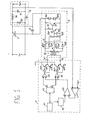
- Fig. 1 shows an ON/OFF control system wherein a swit ching power FET 1, having an intrinsic gate-source capacitance 2, inter mittently transfers electrical energy from a continuous voltage source V IN to a network 3.
- the energy transfer is controlled by a control circuit 4 which, through the driving circuit 5 of the present invention, controls the switching ON/OFF of FET 1 on the grounds of the level reached by a prefixed quan tity within network 3.
- Network 3 comprises a smoothing filter, constitu ted by an inductor 30 and a capacitor 31 and a recycle diode 32. Therefore the system of fig. 1 represents the particular case of a DC regulator and the considerations which will be made for such system are valid even though network 3 be representative of any other circuit.
- the quantity of network 3 which control circuit 4 uses to control the switching of FET 1 is constituted in this case by output voltage V OUT on the ends of capacitor 31.
- Control circuit 4 is practically a pulse width modulator.
- the output of oscillator 40 is connected to the input of a D flip-flop 41 which acts as frequency divider and to the control input of a raw circuit 42.
- the output of ramp circuit 42 is connected to the non-inverting input of a comparator 43 which receives on its inverting input the signal present on the output of an error amplifier 44.
- Amplifier 44 receives on its inverting and non-inverting input output voltage V OUT and a reference voltage V RET respectively and provides on its output a signal proportional to the deviation of voltage V OUT as to voltage V .
- comparator 43 provides on its output a series of pulses whose length depends on the error signal on the output of amplifier 44.
- comparator 43 The output of comparator 43 is connected to an input of 2 two-input OR gates 45, 46.
- OR gates 45, 46 are connected to outputs Q, Q of flip-flop 41. respectively.
- OR gate 45 is connected to the base of a transistor 47B and, through a NOT gate 45A, to the base of a transistor 47A.
- Transistor 47A, 47B are connected in series between a supply voltage +V and ground.
- a first output A of circuit 4 is derived from the connection point of the emitter of transistor 47A with the collector of transistor 47B.
- OR gate 45 also the output of OR gate 46 is connected to the base of a transistor 48B and, through a NOT gate 46A, to the base of a transistor 48A.
- transistor 48A, 48B are connected in series between voltage +V and ground.
- a second output B of circuit 4 is derived from the connection point of the emitter of transistor 48A with the collector of transistor 48B.
- Fig. 2 shows the wave-forms of sane signals present on sane points of control circuit 4 of fig. 1.
- the pulses in output from control circuit 4 may have a maximum length equal to 50% of their period T.
- driving circuit 5 which constitutes more properly the object of the present invention, includes a driving tran sformer 50 comprising two secondary windings having a common end M. The two ends of the primary winding of transformer 50 are respectively connected to outputs A, B of control circuit 4.
- transformer 50 The primary winding of transformer 50 is therefore supplied with voltage pulses having an alternately positive and negative amplitude, as shown by diagram V AB of fig. 2.
- the free ends of the secondary windings of transformer 50 are connected to the anodes of rectifying diodes 51A, 52A and 51B, 52B respecti_ vely.
- the cathodes of diodes 51A, 51B (52A, 52B) are connected each other in node R(S).
- pulses on nodes R, S may reach a length equal to 100% of their period.
- a voltage divider constituted by a resistor 53A and 53B, is connected between node S and common end M of the secondary windings of transformer 50.
- a capacitor 54 is connected in parallel to resistor 53B to avoid an overvoltage during the rising edges of the driving pulses.
- the common node of resistors 53A, 53B and of capacitor 54 is connected to the base of a bipolar transistor 55 having the emitter connected to common end M.
- the collector of transistor 55 is connected to node R through a resistor 56 and to the base of a transistor 57 having the emitter and the collector respectively connected to common end M and to node R.
- Node R and end M are also respectively connected to the gate and to the source of FET 1, that is to the ends of intrinsic capacitance 2.
- Two Zener protection diodes 58A, 58B avoid that the voltage between the ends of capacitance 2 exceeds or falls below a prefixed value. The working of the described driving circuit is very simple.
- Intrinsic capacitance 2 charges very fast and switches ON FET11.
- the driving pulse keeps up the charge of capacitance 2 during all the time when it is at logical/electrical level 1.
- transistor 55 is switched OFF.
- node R remains to logical/electrical level 1 owing to the charge voltage of capacitance 2.
- transistor 57 is immediately switched ON and capacitance 2 discharges very fast.
- fig. 3 shows a possible variant of the driving circuit of the present invention.
- one of fig. 3 presents on only couple of rectifying diodes 59A, 59B and an additional diode 60 which prevents the discharging of capacitance 2 through the voltage divider constituted by resistors 53A, 53B when the driving pul se on node Z falls to logical/electrical level O.
- the voltage in output from the diode bridge is therefore completely equivalent to that one available between node Z and M of fig. 3.
- a further obvious change is that one of replacing bipolar transistors 55, 57 of fig. 1 and 3 with a couple of complementary transistors in push-pull configuration.
Landscapes
- Engineering & Computer Science (AREA)
- Power Engineering (AREA)
- Dc-Dc Converters (AREA)
- Electronic Switches (AREA)
Priority Applications (3)
| Application Number | Priority Date | Filing Date | Title |
|---|---|---|---|
| DE8484101753T DE3469330D1 (en) | 1984-02-20 | 1984-02-20 | Power fet driving circuit |
| EP84101753A EP0153423B1 (de) | 1984-02-20 | 1984-02-20 | Treiberschaltung für einen Leistungs-FET |
| US06/696,987 US4634903A (en) | 1984-02-20 | 1985-01-31 | Power FET driving circuit |
Applications Claiming Priority (1)
| Application Number | Priority Date | Filing Date | Title |
|---|---|---|---|
| EP84101753A EP0153423B1 (de) | 1984-02-20 | 1984-02-20 | Treiberschaltung für einen Leistungs-FET |
Publications (2)
| Publication Number | Publication Date |
|---|---|
| EP0153423A1 true EP0153423A1 (de) | 1985-09-04 |
| EP0153423B1 EP0153423B1 (de) | 1988-02-10 |
Family
ID=8191785
Family Applications (1)
| Application Number | Title | Priority Date | Filing Date |
|---|---|---|---|
| EP84101753A Expired EP0153423B1 (de) | 1984-02-20 | 1984-02-20 | Treiberschaltung für einen Leistungs-FET |
Country Status (3)
| Country | Link |
|---|---|
| US (1) | US4634903A (de) |
| EP (1) | EP0153423B1 (de) |
| DE (1) | DE3469330D1 (de) |
Cited By (5)
| Publication number | Priority date | Publication date | Assignee | Title |
|---|---|---|---|---|
| EP0305479A4 (en) * | 1987-02-26 | 1991-08-28 | Micropolis Corporation | Winchester disk drive system |
| EP0365618B1 (de) * | 1988-03-10 | 1993-10-20 | General Electric Company | Elektronische steuerschaltungen, elektronisch geschaltete motorsysteme und verfahren |
| EP0637868A3 (de) * | 1993-08-04 | 1995-03-22 | Facind Srl | Spannungsregelvorrichtung, zum Beispiel für Motorräder. |
| US8338758B2 (en) | 2004-06-07 | 2012-12-25 | Advantest Corp. | Heater power control circuit and burn-in apparatus using the same |
| CN105119589A (zh) * | 2014-05-15 | 2015-12-02 | 弗罗纽斯国际有限公司 | 用于操控半导体开关元件的电路布置结构和方法 |
Families Citing this family (34)
| Publication number | Priority date | Publication date | Assignee | Title |
|---|---|---|---|---|
| FR2582880B1 (fr) * | 1985-05-30 | 1992-11-27 | Matra | Dispositif de surveillance d'etat d'un commutateur electrique et relais electrique en comportant application |
| JPS62242413A (ja) * | 1986-04-15 | 1987-10-23 | Mitsubishi Electric Corp | トランジスタのベ−ス駆動回路 |
| US4792746A (en) * | 1987-05-11 | 1988-12-20 | Astec Components, Ltd. | Non-dissipative series voltage switching regulator having improved switching speed |
| US4808839A (en) * | 1988-04-04 | 1989-02-28 | Motorola, Inc. | Power field effect transistor driver circuit for protection from overvoltages |
| US4937722A (en) * | 1988-08-23 | 1990-06-26 | North American Philips Corporation | High efficiency direct coupled switched mode power supply |
| US4859927A (en) * | 1988-10-28 | 1989-08-22 | Fisher Scientific Company | Power supply with improved switching regulator |
| US4887021A (en) * | 1989-01-31 | 1989-12-12 | Honeywell Inc. | Precision noise spike elimination circuit for pulse width modulators and PWM inverters |
| US4961048A (en) * | 1989-08-03 | 1990-10-02 | The United States Of America As Represented By The Secretary Of The Navy | MOSFET switching arrangement in a power converter unit |
| FR2656965B1 (fr) * | 1990-01-09 | 1995-01-20 | Sgs Thomson Microelectronics | Commande et controle d'un commutateur de puissance. |
| USRE36480E (en) * | 1990-01-09 | 2000-01-04 | Stmicroelectronics, S.A. | Control and monitoring device for a power switch |
| US5206540A (en) * | 1991-05-09 | 1993-04-27 | Unitrode Corporation | Transformer isolated drive circuit |
| US5168182A (en) * | 1991-06-24 | 1992-12-01 | United Technologies Corporation | 0-100% duty cycle, transformer isolated fet driver |
| US5430405A (en) * | 1992-08-12 | 1995-07-04 | Lambda Electronics Inc. | Control circuit for converters operating in the discontinuous mode |
| JPH0732941A (ja) * | 1993-07-15 | 1995-02-03 | Alps Electric Co Ltd | 自動車用照明装置の保護回路 |
| US5594631A (en) * | 1994-04-20 | 1997-01-14 | The Boeing Company | Digital pulse width modulator for power supply control |
| US5434528A (en) * | 1994-04-29 | 1995-07-18 | Sundstrand Corporation | Gate drive using continuous alternating power and a diode H-bridge |
| FI96465C (fi) * | 1994-05-16 | 1996-06-25 | Nokia Mobile Phones Ltd | Menetelmä ja kytkentäjärjestely kannettavan laitteen ladattavien akkujen laturin tunnistamiseksi |
| US5635867A (en) * | 1994-07-20 | 1997-06-03 | Lucent Technologies Inc. | High performance drive structure for MOSFET power switches |
| US5786687A (en) * | 1996-12-03 | 1998-07-28 | Compaq Computer Corporation | Transformer-isolated pulse drive circuit |
| US5903173A (en) * | 1997-05-12 | 1999-05-11 | Caterpillar Inc. | Low side driver circuit with diagnostic output |
| US5900683A (en) * | 1997-12-23 | 1999-05-04 | Ford Global Technologies, Inc. | Isolated gate driver for power switching device and method for carrying out same |
| US6553117B1 (en) * | 1998-06-29 | 2003-04-22 | Cisco Technology, Inc. | Programmable multiple-standard digital communications system |
| CA2687307A1 (en) * | 1999-04-26 | 2000-10-26 | S&C Electric Company | Control arrangement and method for electronic device |
| TW441840U (en) * | 1999-07-15 | 2001-06-16 | Via Tech Inc | Voltage switched regulator |
| DE19953884A1 (de) * | 1999-11-09 | 2001-05-23 | Infineon Technologies Ag | Schaltungsanordnung zur Erzeugung von Signalformen |
| US6978386B2 (en) | 2000-12-28 | 2005-12-20 | Ge Fanuc Automation North America, Inc. | Method and apparatus for regulating current for programmable logic controllers |
| TW595077B (en) * | 2002-04-03 | 2004-06-21 | Int Rectifier Corp | Synchronous buck converter improvements |
| WO2007138509A2 (en) * | 2006-05-29 | 2007-12-06 | Koninklijke Philips Electronics N.V. | Switching circuit arrangement |
| DE202009002383U1 (de) * | 2009-02-20 | 2009-04-23 | Nucon GbR: Gert G. Niggemeyer & Jörg Niggemeyer (vertretungsberechtigter Gesellschafter: Herr Jörg Niggemeyer, 21244 Buchholz) | Schaltung zur potenzialfreien Ansteuerung mit entgegen gerichteten Signalen mittels eines Übertragers |
| CN103337963A (zh) * | 2013-07-16 | 2013-10-02 | 南京航空航天大学 | 一种占空比分合式变压器隔离驱动电路 |
| CN104716816A (zh) * | 2013-12-17 | 2015-06-17 | 台达电子企业管理(上海)有限公司 | 功率转换装置、隔离驱动电路与隔离驱动方法 |
| JP7359016B2 (ja) * | 2020-02-10 | 2023-10-11 | Tdk株式会社 | 駆動回路 |
| CN113315374B (zh) * | 2021-05-28 | 2022-07-26 | 电子科技大学 | 一种基于Buck变换器的占空比调制脉冲序列控制方法及装置 |
| WO2025022733A1 (ja) * | 2023-07-25 | 2025-01-30 | パナソニックIpマネジメント株式会社 | 駆動回路および動作方法 |
Citations (1)
| Publication number | Priority date | Publication date | Assignee | Title |
|---|---|---|---|---|
| EP0053709A2 (de) * | 1980-12-04 | 1982-06-16 | Siemens Aktiengesellschaft | Schaltungsanordnung zum Ansteuern mindestens eines Leistungs-FET |
Family Cites Families (2)
| Publication number | Priority date | Publication date | Assignee | Title |
|---|---|---|---|---|
| US4438356A (en) * | 1982-03-24 | 1984-03-20 | International Rectifier Corporation | Solid state relay circuit employing MOSFET power switching devices |
| US4492883A (en) * | 1982-06-21 | 1985-01-08 | Eaton Corporation | Unpowered fast gate turn-off FET |
-
1984
- 1984-02-20 EP EP84101753A patent/EP0153423B1/de not_active Expired
- 1984-02-20 DE DE8484101753T patent/DE3469330D1/de not_active Expired
-
1985
- 1985-01-31 US US06/696,987 patent/US4634903A/en not_active Expired - Fee Related
Patent Citations (1)
| Publication number | Priority date | Publication date | Assignee | Title |
|---|---|---|---|---|
| EP0053709A2 (de) * | 1980-12-04 | 1982-06-16 | Siemens Aktiengesellschaft | Schaltungsanordnung zum Ansteuern mindestens eines Leistungs-FET |
Non-Patent Citations (4)
| Title |
|---|
| ELEKTRONIK vol. 32, no. 12, June 1983, München; W. HORN "Leistungs-mosfet potentialfrei angesteuert", page 67 * |
| FRANZIS PROFESSIONELLE ELEKTRONIK D. NÜHRMANN "Stromversorgungs-schaltungen, Triac- und Zündschaltungen" 1984, FRANZIS-VERLAG GMBH, München pages 182-189 * |
| NEW ELECTRONICS vol. 16, no. 6, March 1983, London, GB; L. HARMAN "Coupling p.w.m. drive waveforms", page 28 * |
| Patent Abstracts of Japan vol. 7, no. 247, 2 November 1983 & JP-A-58-136137 * |
Cited By (6)
| Publication number | Priority date | Publication date | Assignee | Title |
|---|---|---|---|---|
| EP0305479A4 (en) * | 1987-02-26 | 1991-08-28 | Micropolis Corporation | Winchester disk drive system |
| EP0365618B1 (de) * | 1988-03-10 | 1993-10-20 | General Electric Company | Elektronische steuerschaltungen, elektronisch geschaltete motorsysteme und verfahren |
| EP0637868A3 (de) * | 1993-08-04 | 1995-03-22 | Facind Srl | Spannungsregelvorrichtung, zum Beispiel für Motorräder. |
| US8338758B2 (en) | 2004-06-07 | 2012-12-25 | Advantest Corp. | Heater power control circuit and burn-in apparatus using the same |
| CN105119589A (zh) * | 2014-05-15 | 2015-12-02 | 弗罗纽斯国际有限公司 | 用于操控半导体开关元件的电路布置结构和方法 |
| CN105119589B (zh) * | 2014-05-15 | 2018-04-27 | 弗罗纽斯国际有限公司 | 用于操控半导体开关元件的电路布置结构和方法 |
Also Published As
| Publication number | Publication date |
|---|---|
| DE3469330D1 (en) | 1988-03-17 |
| EP0153423B1 (de) | 1988-02-10 |
| US4634903A (en) | 1987-01-06 |
Similar Documents
| Publication | Publication Date | Title |
|---|---|---|
| EP0153423A1 (de) | Treiberschaltung für einen Leistungs-FET | |
| EP0112119B1 (de) | Gleichrichterbrückenschaltung | |
| US3986097A (en) | Bilateral direct current converters | |
| US5726869A (en) | Synchronous rectifier type DC-to-DC converter in which a saturable inductive device is connected in series with a secondary-side switching device | |
| EP0291120B1 (de) | Gesteuerte Hochfrequenzleistungsversorgung | |
| US6201713B1 (en) | Switching power supply unit having sub-switching element and time constant circuit | |
| KR20010014809A (ko) | 직류 전원 회로 | |
| EP1229635B1 (de) | Aktive Gate-Klemmschaltung für selbstgesteuerte Synchrongleichrichter | |
| JPH02114861A (ja) | 断続調整型電源回路 | |
| US4607210A (en) | Potential free actuation circuit for a pulse duration controlled electronic power switch | |
| EP0295858B1 (de) | Hochspannungsgleichstromleistungsversorgung | |
| CZ10493A3 (en) | Network-operated control circuit arrangement with phase control | |
| EP0064483B1 (de) | Hochspannungsumformer | |
| US4607319A (en) | Flyback DC/DC converter with low ripple in the output capacitor | |
| EP0474312B1 (de) | Gleichstromwandler | |
| JP3247109B2 (ja) | スイッチングレギュレータ | |
| US6587357B1 (en) | Method and apparatus for providing integrated low power self-supply in switched mode power supplies | |
| US4744020A (en) | Switching mode power supply | |
| US4353115A (en) | Apparatus for synthesizing a sinusoidal output | |
| FI80552B (fi) | Kopplingsanordning foer laogbrusig matning av impulser som haerroer fraon en sinusformig vaexelspaenning, speciellt 16khz betalningsimpuler. | |
| JP3379556B2 (ja) | スイッチング素子を有する回路装置 | |
| SU892425A1 (ru) | Стабилизированный конвертор | |
| JP2614056B2 (ja) | Dc/dcコンバータ | |
| RU2208894C2 (ru) | Устройство для формирования импульса управления силовым транзистором | |
| US20040022080A1 (en) | Switching transformer |
Legal Events
| Date | Code | Title | Description |
|---|---|---|---|
| PUAI | Public reference made under article 153(3) epc to a published international application that has entered the european phase |
Free format text: ORIGINAL CODE: 0009012 |
|
| 17P | Request for examination filed |
Effective date: 19841210 |
|
| AK | Designated contracting states |
Designated state(s): DE FR GB IT |
|
| 17Q | First examination report despatched |
Effective date: 19860515 |
|
| RAP1 | Party data changed (applicant data changed or rights of an application transferred) |
Owner name: HONEYWELL BULL ITALIA S.P.A. |
|
| GRAA | (expected) grant |
Free format text: ORIGINAL CODE: 0009210 |
|
| ITF | It: translation for a ep patent filed | ||
| AK | Designated contracting states |
Kind code of ref document: B1 Designated state(s): DE FR GB IT |
|
| REF | Corresponds to: |
Ref document number: 3469330 Country of ref document: DE Date of ref document: 19880317 |
|
| ET | Fr: translation filed | ||
| PLBE | No opposition filed within time limit |
Free format text: ORIGINAL CODE: 0009261 |
|
| STAA | Information on the status of an ep patent application or granted ep patent |
Free format text: STATUS: NO OPPOSITION FILED WITHIN TIME LIMIT |
|
| 26N | No opposition filed | ||
| ITTA | It: last paid annual fee | ||
| PGFP | Annual fee paid to national office [announced via postgrant information from national office to epo] |
Ref country code: DE Payment date: 19920120 Year of fee payment: 9 |
|
| PGFP | Annual fee paid to national office [announced via postgrant information from national office to epo] |
Ref country code: GB Payment date: 19920210 Year of fee payment: 9 |
|
| PGFP | Annual fee paid to national office [announced via postgrant information from national office to epo] |
Ref country code: FR Payment date: 19920226 Year of fee payment: 9 |
|
| PG25 | Lapsed in a contracting state [announced via postgrant information from national office to epo] |
Ref country code: GB Effective date: 19930220 |
|
| GBPC | Gb: european patent ceased through non-payment of renewal fee |
Effective date: 19930220 |
|
| PG25 | Lapsed in a contracting state [announced via postgrant information from national office to epo] |
Ref country code: FR Effective date: 19931029 |
|
| PG25 | Lapsed in a contracting state [announced via postgrant information from national office to epo] |
Ref country code: DE Effective date: 19931103 |
|
| REG | Reference to a national code |
Ref country code: FR Ref legal event code: ST |