EP0153860A2 - Logische Schaltung - Google Patents
Logische Schaltung Download PDFInfo
- Publication number
- EP0153860A2 EP0153860A2 EP85301311A EP85301311A EP0153860A2 EP 0153860 A2 EP0153860 A2 EP 0153860A2 EP 85301311 A EP85301311 A EP 85301311A EP 85301311 A EP85301311 A EP 85301311A EP 0153860 A2 EP0153860 A2 EP 0153860A2
- Authority
- EP
- European Patent Office
- Prior art keywords
- transistor
- gate
- voltage
- load
- driver
- Prior art date
- Legal status (The legal status is an assumption and is not a legal conclusion. Google has not performed a legal analysis and makes no representation as to the accuracy of the status listed.)
- Granted
Links
Images



Classifications
-
- H—ELECTRICITY
- H03—ELECTRONIC CIRCUITRY
- H03K—PULSE TECHNIQUE
- H03K19/00—Logic circuits, i.e. having at least two inputs acting on one output; Inverting circuits
- H03K19/02—Logic circuits, i.e. having at least two inputs acting on one output; Inverting circuits using specified components
- H03K19/08—Logic circuits, i.e. having at least two inputs acting on one output; Inverting circuits using specified components using semiconductor devices
- H03K19/094—Logic circuits, i.e. having at least two inputs acting on one output; Inverting circuits using specified components using semiconductor devices using field-effect transistors
- H03K19/0952—Logic circuits, i.e. having at least two inputs acting on one output; Inverting circuits using specified components using semiconductor devices using field-effect transistors using Schottky type FET MESFET
-
- H—ELECTRICITY
- H03—ELECTRONIC CIRCUITRY
- H03K—PULSE TECHNIQUE
- H03K19/00—Logic circuits, i.e. having at least two inputs acting on one output; Inverting circuits
- H03K19/01—Modifications for accelerating switching
- H03K19/017—Modifications for accelerating switching in field-effect transistor circuits
- H03K19/01707—Modifications for accelerating switching in field-effect transistor circuits in asynchronous circuits
-
- H—ELECTRICITY
- H03—ELECTRONIC CIRCUITRY
- H03K—PULSE TECHNIQUE
- H03K3/00—Circuits for generating electric pulses; Monostable, bistable or multistable circuits
- H03K3/02—Generators characterised by the type of circuit or by the means used for producing pulses
- H03K3/353—Generators characterised by the type of circuit or by the means used for producing pulses by the use, as active elements, of field-effect transistors with internal or external positive feedback
- H03K3/356—Bistable circuits
- H03K3/356017—Bistable circuits using additional transistors in the input circuit
- H03K3/356052—Bistable circuits using additional transistors in the input circuit using pass gates
- H03K3/35606—Bistable circuits using additional transistors in the input circuit using pass gates with synchronous operation
Definitions
- the present invention relates to a logic circuit, such as an inverter circuit, which is formed by a junction type or a Schottky barrier gate type field effect transistor (FET).
- a logic circuit such as an inverter circuit, which is formed by a junction type or a Schottky barrier gate type field effect transistor (FET).
- FET Schottky barrier gate type field effect transistor
- MOS type FET's are widely used in the conventional Si substrate at present, because this enables an enhancement type FET to be easily manufactured.
- depletion type,and enhancement type FET's are used as load resistors in inverter circuits widely used in logic circuits, but an enhancement type FET is more usually used as a driver transistor.
- a junction type FET can be transformed into an enhancement type FET (strictly speaking, the normally OFF type FET) by decreasing the total amount of impurities therein.
- junction type FET Some problems arise in the design and manufacture of logic circuits using the junction type FET. For example: 1 it is necessary to strictly control the threshold voltage of the FET's (+0.01 V), and 2 the logic amplitude cannot be increased, because a forward voltage larger than a built-in voltage (0.7 V in the GaAs Schottky type junction) cannot be applied to a gate junction.
- the use of the junction type FET has the following advantages; 1 the logic amplitude is small and thus the electric power dissipation is low and the operation speed becomes high, and 2 an ultra high speed IC can be obtained by using a material other than Si for the semiconductor substrate.
- An / of the present invention can provide a logic circuit formed by junction type or Schottky barrier type gate FET's which can eliminate the above- mentioned drawbacks.
- An /embodiment of the present invention can provide a logic circuit having a characteristic similar to that wherein a MOSFET is used by restricting the range of the gate voltage of a load FET.
- An embodiment of the present invention can provide a memory circuit having a bit line pull-up circuit which does not cause memory cell transistors to oe destroyed.
- a logic circuit comprising a driver transistor and a load transistor formed by a junction type or Schottky barrier type FET, an input terminal connected tc a gate of the driver transistor, and a gate voltage generator which is connected to a gate of the load transistor and which generates a level higher than the sum of threshold values of the load transistor and the driver transistor and lower than a low value among the first sum of a built-in voltage of the load transistor and the threshold voltage of the driver transistor and the second sum of a built-in voltage of the driver transistor and the threshold voltage of the load transistor.
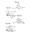
- Figure lA shows a construction of an inverter circuit formed by a usual n channel MOSFET, in which Q l is a driver FET, Q 2 is a load FET, and all transistors are enhancement type.
- V IN is an input terminal
- V OUT is an output terminal
- V DD is an electric source
- COM is a common ground.
- the load FET Q 2 is a MOS diode in which the gate and drain are connected together, and when V DD is higher than a specified value, the load FET Q 2 is placed in an ON state. In this circuit, a forward rising voltage varies due to the threshold voltage of the FET Q 2 .
- A shows a drain I-V characteristic curve of the FET Q l , wherein the x axis shows a voltage V DS between a drain and a source, and the Y axis shows a drain current I D ; Vth 1 designates a threshold voltage of the FET Q 1 ; and B designates a load curve of the MOSFET Q 2 .
- This V-I characteristic varies depending on the following equation (square characteristic): Wherein I L is a load current, i.e., the current in FET Q 2 , the output V OUT is determined by the cross-point of lines A and B, and a desired amplitude output is obtained by suitably selecting the threshold voltage Vth 2 of the load FET Q 2 .
- a load FET Q 4 is operated as a simple diode, and the load characteristic does not change even if the threshold voltage of FET /Q 4 is changed. That is, as shown in Fig. 2B, curve A shows the I-V characteristic curve of FET Q 3 , and curve B shows a load line due to FET Q 4 .
- the solid line of the load curve B shows the state where VDD - V OUT ⁇ V bi (V bi is a built-in voltage), and in this case, the gate current does not flow and the V-I characteristic varies, as for a MOSFET, depending on the following equation:
- the same amplitude can be obtained as from the inverter circuit formed by a MOSFET.
- V DD becomes high and the load curve becomes as shown by the dotted line in Fig. 2B
- the amplitude that is, an output change
- the logic level of the input V IN is 0 ⁇ V bi
- the logic level of the output V OUT depends on the electric source voltage V DD and is in the range of ( V DD - V bi ) ⁇ V DD . Therefore, when the input and the output logic levels are set, it is necessary to set V DD ⁇ V bi so that the level of V DD can be set at a high level.
- FIGS. 3A to 3F are diagrams explaining these constructions.
- Figs. 3A and 3B show Schottky barrier gate and junction type FET's (hereinafter calle collectively junction type), and
- Fig. 3C shows a MOSFET.
- the substrate 1 of the junction type FET is formed by GaAs and is insulative, so that impurities are doped in the source, drain, and channel regions to effect conductivity, and a source electrode S and a drain electrode D are attached to the source and drain regions n , n , and a gate electrode G is attached to the channel region n.
- the substrate 2 of the MOSFET shown in Fig. 3C is made from Si, however, it differs in that a gate oxide film (SiO 2 ) 3_is sandwiched between the gate electrode G and the substrate 2.
- Figure 3D shows a characteristic between the drain-source voltage V DS of the Schottky barrier type FET and the drain current I D
- Fig. 3E shows a characteristic between the drain-source voltage V DS of the junction type FET and the drain current I D .
- the gate voltage is used as the parameter.
- Figure 3F shows the voltage current characteristic of the gate of the junction type FET, when the gate voltage V is raised higher than the predetermined voltage, a gate junction current flows. This is a characteristic of the diode.
- FIG. 4A is a circuit diagram of one embodiment of the present invention, wherein reference numeral 1 designates a gate voltage generator and transistors Q 5 , Q 6 are normally OFF type junction FET's.
- the constants of the driving FET Q S are B 1 , Vth 1
- the constants of FET Q 6 are B 2 , Vth 2
- V out (max) V R - Vth 2 (3) Therefore, from the following equation (3), it can be seen that the maximum value V out (max) of the output voltage can be controlled by the gate voltage V R .
- V bi designates a built-in voltage of the next stage transistor Q 5a . That is, the H level of the output voltage should be equal or lower than the V bi of the transistor Q 5a so that there is no gate current of the transistor Q 5a . Therefore, V out (max) ⁇ V bi , combined with equation (3),
- V R V bi + Vth 2 (4)
- the minimum value of the high level output voltage that is, the voltage for making the next stage transistor Q 5a (off)
- Vth 1 Vth 1
- the load characteristic shown in Figs. 4B becomes the same as that of the MOSFET.
- the transistor Q 5a would not be destroyed by the gate current.
- the low level of V out is clamped at the level V R - V b i; because if the V out becomes lower than V R - V bi , the gate junction or barrier of the load FET Q6 turns on. And also, the low level of V out should be lower than Vth 1 of Q 5a . Therefore, V R - V bi ⁇ V L ⁇ Vth 1 .
- FIG. 5 and 6 show concrete examples of the gate voltage generator 1 shown in Fig. 4A.
- the transistor Q 7 is a driver FET and Q 8 is a load transistor and Q 7a , Q 8a are the next stage FET's.
- the value V bi of the Schottky type transistor is +0.7 V
- V DD +2 V
- the output voltage V out becomes 0.7 volt
- the output voltage V out becomes 0.1 volt.
- Q 10 is a driver FET
- Q 11 is a load FET
- Q 10a and Q lla form the next stage inverter.
- both are GaAs MESFET's as in Fig. 5.
- the built-in voltage thereof is +0.7 volt.
- V IN when V IN is 0.1 V, V out becomes 0.7 V, and when V IN is 0.7 V, V out becomes 0 V, so that the gate of the load FET is not conductive, and a characteristic similar to that of Fig. 5 can be obtained.
- FIG. 7 is a modification of the embodiment of Fig. 5, in which the load gate voltage V R is generated by a constant current source using a depletion type FET Q31 and a diode Q 32 (forward built-in voltage V bi ) formed by shcrting between a drain and a source of the junction type FET.
- V bi forward built-in voltage
- the equation (4) can be satisfied.
- the gate voltage V R generated by using the diode as shown in Fig. 7 has a greater precision than that generated by using the resistor as shown in Fig. 5.
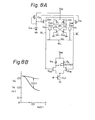
- Figure 8A shews an embodiment of the present invention when applied to a bit line pull up circuit in a static memory, wherein BL, BL are bit lines, WL is a word line.
- Q 21 and Q 22 are driver FET's
- Q 23 and Q24 are internal load FET's for forming a flip-flop circuit together with the drivers Q 21 and Q 22
- Q25 and Q 26 are transfer FET's.
- Q 27 and Q 28 are bit line pull up FET's. Therefore, pairs of transistors Q 27 and Q21 , and Q 28 and Q 22 form the inverter circuit as shown in Fig. 4A.
- the gates are all 1 ⁇ m, in length the gate width of Q 21 ' Q 22 , Q 25 , and Q 26 is 10 ⁇ m, the gate width of Q 23 , and Q 24 is 2 pm, and the gate width of Q 27 and Q 28 is 20 ⁇ m.
- the circuit shown in Fig. 7 is used as the gate voltage generator. Further, in Fig.-8, FET's Q 35 and Q 36 are sense amplifiers, and an FET Q 37 is provided for selecting the bit lines BL, BL.
- This can be achieved by setting the voltage V R so as to satisfy the equation (6), (7). That is, before turning on the transfer gate Q26 , the bit line BL level V4 is lower than V bi of Q 21 according to the equation (6). Therefore, the V 4 level is lower than V 2 so that after turning on the transfer gate Q 26 , there is no big current from the bit line BL to the gate of the transistor Q 21 consequently, no destruction of Q 21 .
- the voltage V 3 falls only to V DD - V bi , and a potential difference exists between V 3 and V 1 , whereby the current flows into the memory cell via the FET. If this current becomes larger than a specified value, the state of the memory cell is inverted. Further, when the voltage V 4 rises to V DD , the current flows via the FET Q 26 into the memory cell. This current flows from the gate to the source of the FET Q 21 , and may melt the gate of the FET. However, this can be prevented by ensuring that the voltage V R satisfies the equation (4).
- Figure 9A is the conventional circuit using depletion type FET's in which the gate and the source of the FET's Q 27 , Q28 are connected.
- the amplitude of the output voltage can be increased.
- the stray capacitance of the bit line is larger, therefore, when the amplitude voltage is increased, the switching speed is decreased because of the length of the charge and the discharge time. To increase the switching speed, the amplitude must be set as small as possible. In the circuit shown in Fig.
- this value of the amplitude can be set lower than V bi .
- the built-in voltage V bi is determined by the construction and the material of the gate junction of the FET, and has a good reproducibility.
- the load gate voltage V R is decreased, the amplitude becomes further decreased, and a higher speed operation can be obtained.
- the difference between the bit lines is in the order of 0.2 V, that is, it is only one-sixth of that shown in Fi g . 9B. Because this output amplitude is small, however, a sufficient noise margin is allowable, and the operation speed becomes high, i.e., a three-fold increase when compared to the case shown in Fig. 9B.
- an inverter circuit having an E-E construction due to inclusion of the junction type FET can be operated in the same manner as an inverter circuit using a MOSFET, and high speed operation can be obtained because of the small output amplitude. Further, the amplitude of the output voltage is made smaller than the built-in voltage of the gate junction, and thus there is no danger of a flow of the gate current into the next stage junction type FET, and therefore, it is very effective for the realization of a high speed IC using a GaAs semiconductor substrate.
Landscapes
- Engineering & Computer Science (AREA)
- Physics & Mathematics (AREA)
- Computer Hardware Design (AREA)
- Computing Systems (AREA)
- General Engineering & Computer Science (AREA)
- Mathematical Physics (AREA)
- Power Engineering (AREA)
- Logic Circuits (AREA)
- Static Random-Access Memory (AREA)
- Junction Field-Effect Transistors (AREA)
Applications Claiming Priority (2)
| Application Number | Priority Date | Filing Date | Title |
|---|---|---|---|
| JP59037460A JPS60182759A (ja) | 1984-02-29 | 1984-02-29 | 論理回路 |
| JP37460/84 | 1984-02-29 |
Publications (3)
| Publication Number | Publication Date |
|---|---|
| EP0153860A2 true EP0153860A2 (de) | 1985-09-04 |
| EP0153860A3 EP0153860A3 (en) | 1987-09-30 |
| EP0153860B1 EP0153860B1 (de) | 1990-11-14 |
Family
ID=12498133
Family Applications (1)
| Application Number | Title | Priority Date | Filing Date |
|---|---|---|---|
| EP85301311A Expired - Lifetime EP0153860B1 (de) | 1984-02-29 | 1985-02-27 | Logische Schaltung |
Country Status (6)
| Country | Link |
|---|---|
| US (1) | US4656611A (de) |
| EP (1) | EP0153860B1 (de) |
| JP (1) | JPS60182759A (de) |
| KR (1) | KR890004454B1 (de) |
| CA (1) | CA1246694A (de) |
| DE (1) | DE3580496D1 (de) |
Cited By (1)
| Publication number | Priority date | Publication date | Assignee | Title |
|---|---|---|---|---|
| EP0226678A1 (de) * | 1985-12-24 | 1987-07-01 | Fujitsu Limited | Logische Schaltung |
Families Citing this family (1)
| Publication number | Priority date | Publication date | Assignee | Title |
|---|---|---|---|---|
| US6127857A (en) * | 1997-07-02 | 2000-10-03 | Canon Kabushiki Kaisha | Output buffer or voltage hold for analog of multilevel processing |
Family Cites Families (3)
| Publication number | Priority date | Publication date | Assignee | Title |
|---|---|---|---|---|
| JPS5080734A (de) * | 1973-11-14 | 1975-07-01 | ||
| DE2657561B1 (de) * | 1976-12-18 | 1978-04-13 | Ibm Deutschland | Nachlade-Referenzschaltungsanordnung fuer einen Halbleiterspeicher |
| US4355377A (en) * | 1980-06-30 | 1982-10-19 | Inmos Corporation | Asynchronously equillibrated and pre-charged static ram |
-
1984
- 1984-02-29 JP JP59037460A patent/JPS60182759A/ja active Granted
-
1985
- 1985-02-21 KR KR1019850001065A patent/KR890004454B1/ko not_active Expired
- 1985-02-22 US US06/705,321 patent/US4656611A/en not_active Expired - Lifetime
- 1985-02-26 CA CA000475169A patent/CA1246694A/en not_active Expired
- 1985-02-27 EP EP85301311A patent/EP0153860B1/de not_active Expired - Lifetime
- 1985-02-27 DE DE8585301311T patent/DE3580496D1/de not_active Expired - Lifetime
Non-Patent Citations (3)
| Title |
|---|
| IEEE TRANSACTIONS ON ELECTRON DEVICES, vol. ED-25, no. 6, June 1978, pages 628-639, IEEE, New York, US; R. ZULEEG et al.: "Femtojoule high-speed planar GaAs E-JFET logic" * |
| IEEE TRANSACTIONS ON ELECTRON DEVICES, vol. ED-27, no. 6, June 1980, pages 1074-1091, IEEE, New York, US; K. LEHOVEC et al.: "Analysis of GaAs FET's for integrated logic" * |
| U. Tietze, Ch. Schenk, "Halbleiter-Schaltungstechnik", 5th edition, Springer-Verlag Berlin, Heidelberg, New York 1980, page 155 * |
Cited By (2)
| Publication number | Priority date | Publication date | Assignee | Title |
|---|---|---|---|---|
| EP0226678A1 (de) * | 1985-12-24 | 1987-07-01 | Fujitsu Limited | Logische Schaltung |
| US4707622A (en) * | 1985-12-24 | 1987-11-17 | Fujitsu Limited | GaAs MESFET logic buffers using enhancement and depletion FETs |
Also Published As
| Publication number | Publication date |
|---|---|
| CA1246694A (en) | 1988-12-13 |
| KR850006789A (ko) | 1985-10-16 |
| JPS60182759A (ja) | 1985-09-18 |
| EP0153860B1 (de) | 1990-11-14 |
| EP0153860A3 (en) | 1987-09-30 |
| DE3580496D1 (de) | 1990-12-20 |
| US4656611A (en) | 1987-04-07 |
| KR890004454B1 (ko) | 1989-11-04 |
| JPH0428179B2 (de) | 1992-05-13 |
Similar Documents
| Publication | Publication Date | Title |
|---|---|---|
| US4494016A (en) | High performance MESFET transistor for VLSI implementation | |
| US4952818A (en) | Transmission line driver circuits | |
| US4730129A (en) | Integrated circuit having fuse circuit | |
| US4996443A (en) | Integrated circuit for level shift | |
| CA1058325A (en) | Enhancement-and depletion-type field effect transistors connected in parallel | |
| EP0143699A2 (de) | Bus-Sender/Empfänger | |
| US4678940A (en) | TTL compatible merged bipolar/CMOS output buffer circuits | |
| US4810969A (en) | High speed logic circuit having feedback to prevent current in the output stage | |
| US5420526A (en) | Circuit for pulling an integrated circuit input to a determined state | |
| US4408245A (en) | Protection and anti-floating network for insulated-gate field-effect circuitry | |
| US4071784A (en) | MOS input buffer with hysteresis | |
| EP0350879B1 (de) | Ausgangstreiberschaltung für Halbleiter-IC | |
| US4578694A (en) | Inverter circuit provided with gate protection | |
| EP0222369B1 (de) | Torschaltung | |
| EP0361546B1 (de) | Halbleiterspeichereinrichtung | |
| EP0281113B1 (de) | Halbleiter - Pufferschaltung | |
| GB1595143A (en) | Fet inverter circuits | |
| US4743957A (en) | Logic integrated circuit device formed on compound semiconductor substrate | |
| US5872733A (en) | Ramp-up rate control circuit for flash memory charge pump | |
| US5374862A (en) | Super buffer and DCFL circuits with Schottky barrier diode | |
| US4656611A (en) | Logic circuit | |
| US5656956A (en) | Logic gate circuit and digital integrated circuit | |
| US5406215A (en) | Open drain driver circuit which eliminates overshoot caused by parasitic capacitances | |
| US4935647A (en) | Group III - V semiconductor devices with improved switching speeds | |
| EP0720296B1 (de) | Pufferschaltung und Vorspannungsschaltung |
Legal Events
| Date | Code | Title | Description |
|---|---|---|---|
| PUAI | Public reference made under article 153(3) epc to a published international application that has entered the european phase |
Free format text: ORIGINAL CODE: 0009012 |
|
| AK | Designated contracting states |
Designated state(s): DE FR GB IT |
|
| PUAL | Search report despatched |
Free format text: ORIGINAL CODE: 0009013 |
|
| AK | Designated contracting states |
Kind code of ref document: A3 Designated state(s): DE FR GB IT |
|
| 17P | Request for examination filed |
Effective date: 19871103 |
|
| 17Q | First examination report despatched |
Effective date: 19890526 |
|
| ITF | It: translation for a ep patent filed | ||
| GRAA | (expected) grant |
Free format text: ORIGINAL CODE: 0009210 |
|
| AK | Designated contracting states |
Kind code of ref document: B1 Designated state(s): DE FR GB IT |
|
| ET | Fr: translation filed | ||
| REF | Corresponds to: |
Ref document number: 3580496 Country of ref document: DE Date of ref document: 19901220 |
|
| PLBE | No opposition filed within time limit |
Free format text: ORIGINAL CODE: 0009261 |
|
| STAA | Information on the status of an ep patent application or granted ep patent |
Free format text: STATUS: NO OPPOSITION FILED WITHIN TIME LIMIT |
|
| 26N | No opposition filed | ||
| ITTA | It: last paid annual fee | ||
| PGFP | Annual fee paid to national office [announced via postgrant information from national office to epo] |
Ref country code: FR Payment date: 20010213 Year of fee payment: 17 |
|
| PGFP | Annual fee paid to national office [announced via postgrant information from national office to epo] |
Ref country code: GB Payment date: 20010221 Year of fee payment: 17 Ref country code: DE Payment date: 20010221 Year of fee payment: 17 |
|
| REG | Reference to a national code |
Ref country code: GB Ref legal event code: IF02 |
|
| PG25 | Lapsed in a contracting state [announced via postgrant information from national office to epo] |
Ref country code: GB Free format text: LAPSE BECAUSE OF NON-PAYMENT OF DUE FEES Effective date: 20020227 |
|
| PG25 | Lapsed in a contracting state [announced via postgrant information from national office to epo] |
Ref country code: DE Free format text: LAPSE BECAUSE OF NON-PAYMENT OF DUE FEES Effective date: 20020903 |
|
| GBPC | Gb: european patent ceased through non-payment of renewal fee |
Effective date: 20020227 |
|
| PG25 | Lapsed in a contracting state [announced via postgrant information from national office to epo] |
Ref country code: FR Free format text: LAPSE BECAUSE OF NON-PAYMENT OF DUE FEES Effective date: 20021031 |
|
| REG | Reference to a national code |
Ref country code: FR Ref legal event code: ST |