EP0154796A2 - Procédé de fabrication d'un empilement de plaques multicanaux métalliques pour intensificateur d'images et utilisation de plaques ainsi fabriquées - Google Patents
Procédé de fabrication d'un empilement de plaques multicanaux métalliques pour intensificateur d'images et utilisation de plaques ainsi fabriquées Download PDFInfo
- Publication number
- EP0154796A2 EP0154796A2 EP85101037A EP85101037A EP0154796A2 EP 0154796 A2 EP0154796 A2 EP 0154796A2 EP 85101037 A EP85101037 A EP 85101037A EP 85101037 A EP85101037 A EP 85101037A EP 0154796 A2 EP0154796 A2 EP 0154796A2
- Authority
- EP
- European Patent Office
- Prior art keywords
- layers
- produced
- plates
- intermediate layers
- negative
- Prior art date
- Legal status (The legal status is an assumption and is not a legal conclusion. Google has not performed a legal analysis and makes no representation as to the accuracy of the status listed.)
- Granted
Links
Images

Classifications
-
- H—ELECTRICITY
- H01—ELECTRIC ELEMENTS
- H01J—ELECTRIC DISCHARGE TUBES OR DISCHARGE LAMPS
- H01J43/00—Secondary-emission tubes; Electron-multiplier tubes
- H01J43/04—Electron multipliers
- H01J43/06—Electrode arrangements
- H01J43/18—Electrode arrangements using essentially more than one dynode
- H01J43/24—Dynodes having potential gradient along their surfaces
- H01J43/246—Microchannel plates [MCP]
-
- H—ELECTRICITY
- H01—ELECTRIC ELEMENTS
- H01J—ELECTRIC DISCHARGE TUBES OR DISCHARGE LAMPS
- H01J9/00—Apparatus or processes specially adapted for the manufacture, installation, removal, maintenance of electric discharge tubes, discharge lamps, or parts thereof; Recovery of material from discharge tubes or lamps
- H01J9/02—Manufacture of electrodes or electrode systems
- H01J9/12—Manufacture of electrodes or electrode systems of photo-emissive cathodes; of secondary-emission electrodes
- H01J9/125—Manufacture of electrodes or electrode systems of photo-emissive cathodes; of secondary-emission electrodes of secondary emission electrodes
-
- H—ELECTRICITY
- H01—ELECTRIC ELEMENTS
- H01J—ELECTRIC DISCHARGE TUBES OR DISCHARGE LAMPS
- H01J2201/00—Electrodes common to discharge tubes
- H01J2201/32—Secondary emission electrodes
Definitions
- the invention relates to a method for producing layered multi-channel plates with metal dynodes for amplifying optical images or other areal signal distributions by means of secondary electron multiplication, and to the use of multi-channel plates produced in this way.
- the invention is based on the object of proposing a method for producing layered multi-channel image intensifier plates of the generic type in which the separate production of the dynodes and their subsequent stacking and mutual alignment are avoided.
- layered multi-channel plates with metal dynodes can be produced, with which a similarly high spatial resolution and a similarly high transparency as in the known image intensifier plates made of glass can be achieved without the limitations typical for glass image intensifier plates in the gain factor and in the signal repetition frequency must be accepted.
- the method of the invention can be modified in accordance with claim 2 to reduce the cost of mass production of multi-channel plates of the type described in claim 1.
- a metallic positive mold is produced with a primary negative mold of the layered multi-channel plate using a metal electrode connected to it by galvanic molding and subsequent removal of the primary negative mold, after which several secondary moldings are made by repeated molding of the metallic positive mold
- Negative forms of the layered multi-channel plate be produced that take on the role of the primary negative form in the further implementation of the method.
- Non-adhesive reactive resins are particularly suitable as impression materials. Further details relating to the impression can be found, for example, in DE-PS 32 06 820.
- the dynodes are mutually electrically isolated by removing the intermediate layers. If layered multi-channel plates with a larger diameter are to be produced in this way, it can be advantageous to mount electrically insulating supports not only on the channel-free edge, but also within the image field of the multi-channel plate, which is penetrated by channels.
- the supports in the area of the layered multi-channel plates, which are interspersed with channels only cover about 1 per mille of the image field, they can be perceived as a disadvantage if the transmission quality is particularly high.
- a modification of the method of the invention according to claim 4 is provided.
- Aluminum is particularly suitable for the subsequent conversion of the intermediate layer into an electrical insulator described there.
- the small wall thicknesses typical of multi-channel plates with high transparency it can be converted in a known manner with oxidizing agent working in the liquid and / or gaseous phase into the electrically excellent insulating Al 2 O 3 .
- the area penetrated by channels is to be surrounded by a channel-free area to facilitate assembly or the electrical connections, this area must consist of numerous thin walls to ensure the conversion of the more easily oxidizable material into an insulator.
- the limitation to thin walls does not apply if the intermediate layers, according to claim 5, are produced by complete or partial oxidation of electrodeposited aluminum layers.
- the oxidation of the aluminum layers can be carried out both chemically and electrochemically.
- an inclination of the channels against the plate surface favors the collision of the primary particles with the channel walls and thus the desired electron release.
- the inclination of the channels is achieved by mutual displacement of the dynodes during stacking.
- dislocations occur between the mutually assigned channels of the adjacent dynodes, which lead to a reduction in transparency and / or the spatial resolution.
- the inclination of the channels can be brought about by appropriate orientation of the plate surface with respect to the direction of propagation of the high-energy radiation without loss of transparency and / or spatial resolution.
- a channel curvature aimed at suppressing the acceleration of parasitic ions can likewise only be achieved in the previously known methods for producing layered multi-channel plates only by mutually displacing the dynodes with the disadvantages mentioned above.
- these disadvantages can be avoided in that, according to claim 7, before the formation of the dynodes and intermediate layers, the negative shapes of the channels are bent at a higher temperature by a uniformly acting force, for example a centrifugal force.
- the layered multi-channel plates can be assembled in such a way that the channel openings of layered multi-channel plates lying on top of one another are aligned with one another. This avoids losses in transparency and / or spatial resolution.
- Both corpuscular rays and electromagnetic waves can be considered as high-energy radiation. While the use of electromagnetic waves to produce the desired structures uses masks in a known manner, the structures can also be generated by electromagnetic control when using corpuscular beams.
- the X-ray radiation (“synchrotron radiation") generated by the electron synchrotons, which is characterized by high intensity with a small aperture angle.
- the choice of the material that can be changed by high-energy radiation depends on the type of high-energy radiation, and corresponding regulations can be found, for example, in DE-PS 29 22 642 and DE-OS 32 21 981.
- PMMA polymethyl methacrylate
- the secondary electron yield factor of those with channels can be known in a manner known per se provided metal layers may be increased considerably.
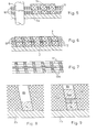
- the PMMA plate 1 is irradiated with synchrotron radiation 3 via an X-ray mask, which is directed obliquely to the surfaces of the PMMA plate 1 and the X-ray mask.
- the x-ray mask consists of a carrier 4 which only weakly absorbs the x-ray radiation and an absorber 5 which strongly absorbs the x-ray radiation, by means of which the cross-sectional shapes and the positions of the negative shapes of the channels are determined.
- the individual structures of the absorber 5 correspond to the cross-sectional shapes of the negative shapes of the channels. Due to the high-intensity parallel synchrotron radiation, the PMMA in the areas 6 not covered by the absorber will undergo chemical radiation changes. These areas 6 irradiated in this way are removed by introducing the PMMA plate into a developer solution, so that a multichannel negative shape with columnar PMMA structures 7 and lattice-shaped free spaces 8 according to FIG. 3 is produced.
- the columnar PMMA structures 7 have a hexagonal cross-sectional shape with a width of approximately 30 ⁇ m , the width of the free spaces 8 between the PMMA structures 7 is approximately 4 ⁇ m.
- FIG. 4 When producing a multi-channel plate with individual dynodes, which are firmly connected to electrically insulating supports, the negative form shown in FIG. 4 is assumed, which, in addition to the metal electrode 2a, the columnar PMMA structures 7a with lattice-free spaces 8a, as they are were already shown in Figure 3, additionally contains supports 9 made of electrically insulating material. In the free spaces 8a layers of nickel 10 and copper 11 are deposited galvanically alternately so that a formed-construction according to "Fig. 5.
- the PMMA structures 7a with an organic solvent and the copper layers 11 and the electrode 2a with an etch, which does not attack the nickel layers 10, are first removed, so that a sequence of mutually insulated dynode layers, which are fixed to the electrically insulating supports 9 connected, remains.
- the negative mold 7 shown in FIG. 3 is used in the production of layered multi-channel plates made of dynodes and intermediate layers subsequently produced. 6, layers of nickel 12 and aluminum 13 are alternately deposited in the free spaces 8 of the negative mold 7. After removal of the negative mold 7 with an organic solvent and the electrode 2 with an etch which does not attack either the nickel layers 12 or the aluminum layers 13, the aluminum layers become known
Landscapes
- Engineering & Computer Science (AREA)
- Manufacturing & Machinery (AREA)
- Electron Tubes For Measurement (AREA)
- Moulds For Moulding Plastics Or The Like (AREA)
- Particle Accelerators (AREA)
- Paper (AREA)
- Pressure Welding/Diffusion-Bonding (AREA)
- Laminated Bodies (AREA)
- Electroplating Methods And Accessories (AREA)
Priority Applications (1)
| Application Number | Priority Date | Filing Date | Title |
|---|---|---|---|
| AT85101037T ATE38451T1 (de) | 1984-03-10 | 1985-02-01 | Verfahren zur herstellung geschichteter vielkanalplatten aus metall fuer bilderverstaerker und verwendung der so hergestellten vielkanalplatten. |
Applications Claiming Priority (2)
| Application Number | Priority Date | Filing Date | Title |
|---|---|---|---|
| DE3408849A DE3408849C2 (de) | 1984-03-10 | 1984-03-10 | Verfahren zur Herstellung geschichteter Vielkanalplatten aus Metall für Bildverstärker und Verwendung der so hergestellten Vielkanalplatten |
| DE3408849 | 1984-03-10 |
Publications (3)
| Publication Number | Publication Date |
|---|---|
| EP0154796A2 true EP0154796A2 (fr) | 1985-09-18 |
| EP0154796A3 EP0154796A3 (en) | 1986-12-30 |
| EP0154796B1 EP0154796B1 (fr) | 1988-11-02 |
Family
ID=6230129
Family Applications (1)
| Application Number | Title | Priority Date | Filing Date |
|---|---|---|---|
| EP85101037A Expired EP0154796B1 (fr) | 1984-03-10 | 1985-02-01 | Procédé de fabrication d'un empilement de plaques multicanaux métalliques pour intensificateur d'images et utilisation de plaques ainsi fabriquées |
Country Status (6)
| Country | Link |
|---|---|
| US (1) | US4563251A (fr) |
| EP (1) | EP0154796B1 (fr) |
| JP (1) | JPS60208040A (fr) |
| AT (1) | ATE38451T1 (fr) |
| BR (1) | BR8501057A (fr) |
| DE (1) | DE3408849C2 (fr) |
Families Citing this family (11)
| Publication number | Priority date | Publication date | Assignee | Title |
|---|---|---|---|---|
| US5189777A (en) * | 1990-12-07 | 1993-03-02 | Wisconsin Alumni Research Foundation | Method of producing micromachined differential pressure transducers |
| US5206983A (en) * | 1991-06-24 | 1993-05-04 | Wisconsin Alumni Research Foundation | Method of manufacturing micromechanical devices |
| US5190637A (en) * | 1992-04-24 | 1993-03-02 | Wisconsin Alumni Research Foundation | Formation of microstructures by multiple level deep X-ray lithography with sacrificial metal layers |
| US5378583A (en) * | 1992-12-22 | 1995-01-03 | Wisconsin Alumni Research Foundation | Formation of microstructures using a preformed photoresist sheet |
| US5412265A (en) * | 1993-04-05 | 1995-05-02 | Ford Motor Company | Planar micro-motor and method of fabrication |
| GB9717210D0 (en) * | 1997-08-14 | 1997-10-22 | Central Lab Of The Research Co | Electron multiplier array |
| US5943223A (en) * | 1997-10-15 | 1999-08-24 | Reliance Electric Industrial Company | Electric switches for reducing on-state power loss |
| DE10305427B4 (de) * | 2003-02-03 | 2006-05-24 | Siemens Ag | Herstellungsverfahren für eine Lochscheibe zum Ausstoßen eines Fluids |
| GB0307526D0 (en) * | 2003-04-01 | 2003-05-07 | Council Cent Lab Res Councils | Electron multiplier array |
| JP2006524077A (ja) * | 2003-04-01 | 2006-10-26 | カウンシル フォー ザ セントラル ラボラトリー オブ ザ リサーチ カウンシルズ | 大面積検出器およびディスプレイ |
| WO2005006734A1 (fr) * | 2003-07-09 | 2005-01-20 | Council For The Central Laboratory Of The Research Councils | Dispositif de generation d'image faisant appel a un multiplicateur d'electrons a grande surface |
Family Cites Families (9)
| Publication number | Priority date | Publication date | Assignee | Title |
|---|---|---|---|---|
| GB1434053A (en) * | 1973-04-06 | 1976-04-28 | Mullard Ltd | Electron multipliers |
| US4193176A (en) * | 1978-10-30 | 1980-03-18 | Hughes Aircraft Company | Multiple grid fabrication method |
| DE2922642C2 (de) * | 1979-06-02 | 1981-10-01 | Kernforschungszentrum Karlsruhe Gmbh, 7500 Karlsruhe | Verfahren zum Herstellen von Platten für den Aufbau von Trenndüsenelementen |
| DE3007385A1 (de) * | 1980-02-27 | 1981-09-03 | Siemens AG, 1000 Berlin und 8000 München | Verfahren zur kontinuierlichen galvanoplastischen fertigung von praezisionsflachteilen |
| DE3039110A1 (de) * | 1980-10-16 | 1982-05-13 | Siemens AG, 1000 Berlin und 8000 München | Verfahren fuer die spannungsfreie entwicklung von bestrahlten polymethylmetacrylatschichten |
| GB2108314A (en) * | 1981-10-19 | 1983-05-11 | Philips Electronic Associated | Laminated channel plate electron multiplier |
| DE3150257A1 (de) * | 1981-12-18 | 1983-06-30 | Siemens AG, 1000 Berlin und 8000 München | Bildverstaerker |
| DE3206820C2 (de) * | 1982-02-26 | 1984-02-09 | Kernforschungszentrum Karlsruhe Gmbh, 7500 Karlsruhe | Verfahren zum Herstellen von Trenndüsenelementen |
| DE3221981C2 (de) * | 1982-06-11 | 1985-08-29 | Kernforschungszentrum Karlsruhe Gmbh, 7500 Karlsruhe | Verfahren zum Herstellen von aus Trennkörpern mit Abschlußplatten bestehenden Trenndüsenelementen zur Trennung gas- oder dampfförmiger Gemische |
-
1984
- 1984-03-10 DE DE3408849A patent/DE3408849C2/de not_active Expired
-
1985
- 1985-02-01 AT AT85101037T patent/ATE38451T1/de not_active IP Right Cessation
- 1985-02-01 EP EP85101037A patent/EP0154796B1/fr not_active Expired
- 1985-03-06 US US06/708,842 patent/US4563251A/en not_active Expired - Fee Related
- 1985-03-08 BR BR8501057A patent/BR8501057A/pt not_active IP Right Cessation
- 1985-03-11 JP JP60046717A patent/JPS60208040A/ja active Granted
Also Published As
| Publication number | Publication date |
|---|---|
| DE3408849C2 (de) | 1987-04-16 |
| JPS60208040A (ja) | 1985-10-19 |
| BR8501057A (pt) | 1985-10-29 |
| EP0154796B1 (fr) | 1988-11-02 |
| ATE38451T1 (de) | 1988-11-15 |
| JPH0535542B2 (fr) | 1993-05-26 |
| US4563251A (en) | 1986-01-07 |
| EP0154796A3 (en) | 1986-12-30 |
| DE3408849A1 (de) | 1985-09-19 |
Similar Documents
| Publication | Publication Date | Title |
|---|---|---|
| DE2435430C2 (de) | Elektrostatischer Wandler | |
| DE3319311C2 (de) | Verfahren zur Herstellung eines elektroakustischen Wandlers mit feststehender Elektrode und dieser gegenüberstehender Membran | |
| DE4341149C2 (de) | Multipolvorrichtung und Verfahren zum Herstellen einer Multipolvorrichtung | |
| DE3106368C2 (de) | Gleichstrom-Gasentladungsanzeigevorrichtung | |
| DE69608713T2 (de) | Herstellungsverfahren einer Feldemissionsvorrichtung mit wellenförmigen Stützsäulen für hohe Durchschlagsfestigkeit | |
| DE60225995T2 (de) | Strippingsfolie, Verfahren zur Herstellung einer Strippingsfolie und Vorrichtung zur Herstellung einer Strippingsfolie | |
| EP0154796B1 (fr) | Procédé de fabrication d'un empilement de plaques multicanaux métalliques pour intensificateur d'images et utilisation de plaques ainsi fabriquées | |
| EP0154772A1 (fr) | Plaque bipolaire pour appareil comprenant un empilement de cellules électrochimiques à électrolyte solide, et son procédé de fabrication | |
| EP0283773B1 (fr) | Multiplicateur d'électrons secondaires miniaturisé et son procédé de fabrication | |
| DE102010062143A1 (de) | Batterieelektrode und Verfahren zum Herstellen derselben | |
| DE2951287A1 (de) | Verfahren zur herstellung von ebenen oberflaechen mit feinsten spitzen im mikrometer-bereich | |
| DE3026778A1 (de) | Elektrode | |
| DE69601956T2 (de) | Herstellungsverfahren einer säulenförmigen Struktur für Feldemissionsvorrichtungen | |
| EP0154797B1 (fr) | Procédé de fabrication de plaques multicanaux et leur utilisation | |
| DE10256922A1 (de) | Metallischer Separator einer Brenstoffzelle und Verfahren zu dessen Herstellung | |
| DE2454413C2 (fr) | ||
| EP0204198B1 (fr) | Structure de canaux d'un multiplicateur d'électrons | |
| DE1209215B (de) | Sekundaerelektronenvervielfacher und Verfahren zur Herstellung des Vervielfachers | |
| EP0010222B1 (fr) | Plaque de commande pour un écran plat à plasma de reproduction d'image | |
| DE112007002067T5 (de) | Brennstoffzellen-Separator, Verfahren zur Herstellung des Brennstoffzellen-Separators und Brennstoffzelle | |
| DE2639033C3 (de) | Bauteil in mit Ladungsträgerstrahlen arbeitenden elektrischen Vakuumgeräten und Verfahren zu dessen Herstellung | |
| DE2900430C3 (de) | Metallisches Wärmeaustauscherelement und Verfahren zur Herstellung desselben | |
| DE4121151C2 (de) | Leuchtschirm | |
| CH650102A5 (de) | Elektronenroehre mit einer anode und einer elektronenquellenbaugruppe. | |
| DE2632100A1 (de) | Zelle fuer elektrische akkumulatoren mit wenigstens einer loeslichen elektrode |
Legal Events
| Date | Code | Title | Description |
|---|---|---|---|
| PUAI | Public reference made under article 153(3) epc to a published international application that has entered the european phase |
Free format text: ORIGINAL CODE: 0009012 |
|
| AK | Designated contracting states |
Designated state(s): AT CH FR GB IT LI NL SE |
|
| 17P | Request for examination filed |
Effective date: 19850805 |
|
| PUAL | Search report despatched |
Free format text: ORIGINAL CODE: 0009013 |
|
| AK | Designated contracting states |
Kind code of ref document: A3 Designated state(s): AT CH FR GB IT LI NL SE |
|
| 17Q | First examination report despatched |
Effective date: 19880321 |
|
| ITF | It: translation for a ep patent filed | ||
| GRAA | (expected) grant |
Free format text: ORIGINAL CODE: 0009210 |
|
| AK | Designated contracting states |
Kind code of ref document: B1 Designated state(s): AT CH FR GB IT LI NL SE |
|
| REF | Corresponds to: |
Ref document number: 38451 Country of ref document: AT Date of ref document: 19881115 Kind code of ref document: T |
|
| GBT | Gb: translation of ep patent filed (gb section 77(6)(a)/1977) | ||
| ET | Fr: translation filed | ||
| PLBE | No opposition filed within time limit |
Free format text: ORIGINAL CODE: 0009261 |
|
| STAA | Information on the status of an ep patent application or granted ep patent |
Free format text: STATUS: NO OPPOSITION FILED WITHIN TIME LIMIT |
|
| 26N | No opposition filed | ||
| ITTA | It: last paid annual fee | ||
| PGFP | Annual fee paid to national office [announced via postgrant information from national office to epo] |
Ref country code: AT Payment date: 19940224 Year of fee payment: 10 |
|
| PGFP | Annual fee paid to national office [announced via postgrant information from national office to epo] |
Ref country code: GB Payment date: 19941116 Year of fee payment: 11 |
|
| PGFP | Annual fee paid to national office [announced via postgrant information from national office to epo] |
Ref country code: CH Payment date: 19941221 Year of fee payment: 11 |
|
| EAL | Se: european patent in force in sweden |
Ref document number: 85101037.1 |
|
| PG25 | Lapsed in a contracting state [announced via postgrant information from national office to epo] |
Ref country code: AT Effective date: 19950201 |
|
| PGFP | Annual fee paid to national office [announced via postgrant information from national office to epo] |
Ref country code: SE Payment date: 19950216 Year of fee payment: 11 |
|
| PGFP | Annual fee paid to national office [announced via postgrant information from national office to epo] |
Ref country code: NL Payment date: 19950228 Year of fee payment: 11 Ref country code: FR Payment date: 19950228 Year of fee payment: 11 |
|
| PG25 | Lapsed in a contracting state [announced via postgrant information from national office to epo] |
Ref country code: GB Effective date: 19960201 |
|
| PG25 | Lapsed in a contracting state [announced via postgrant information from national office to epo] |
Ref country code: SE Effective date: 19960202 |
|
| PG25 | Lapsed in a contracting state [announced via postgrant information from national office to epo] |
Ref country code: LI Free format text: LAPSE BECAUSE OF NON-PAYMENT OF DUE FEES Effective date: 19960228 Ref country code: CH Free format text: LAPSE BECAUSE OF NON-PAYMENT OF DUE FEES Effective date: 19960228 |
|
| PG25 | Lapsed in a contracting state [announced via postgrant information from national office to epo] |
Ref country code: NL Effective date: 19960901 |
|
| GBPC | Gb: european patent ceased through non-payment of renewal fee |
Effective date: 19960201 |
|
| REG | Reference to a national code |
Ref country code: CH Ref legal event code: PL |
|
| PG25 | Lapsed in a contracting state [announced via postgrant information from national office to epo] |
Ref country code: FR Effective date: 19961031 |
|
| NLV4 | Nl: lapsed or anulled due to non-payment of the annual fee |
Effective date: 19960901 |
|
| REG | Reference to a national code |
Ref country code: FR Ref legal event code: ST |