EP0010222B1 - Plaque de commande pour un écran plat à plasma de reproduction d'image - Google Patents
Plaque de commande pour un écran plat à plasma de reproduction d'image Download PDFInfo
- Publication number
- EP0010222B1 EP0010222B1 EP79103758A EP79103758A EP0010222B1 EP 0010222 B1 EP0010222 B1 EP 0010222B1 EP 79103758 A EP79103758 A EP 79103758A EP 79103758 A EP79103758 A EP 79103758A EP 0010222 B1 EP0010222 B1 EP 0010222B1
- Authority
- EP
- European Patent Office
- Prior art keywords
- control
- plate
- layers
- control plate
- glass solder
- Prior art date
- Legal status (The legal status is an assumption and is not a legal conclusion. Google has not performed a legal analysis and makes no representation as to the accuracy of the status listed.)
- Expired
Links
Images
Classifications
-
- H—ELECTRICITY
- H01—ELECTRIC ELEMENTS
- H01J—ELECTRIC DISCHARGE TUBES OR DISCHARGE LAMPS
- H01J17/00—Gas-filled discharge tubes with solid cathode
- H01J17/02—Details
- H01J17/04—Electrodes; Screens
- H01J17/12—Control electrodes
Definitions
- the invention relates to a control plate for a flat plasma imaging screen, with a carrier plate which carries parallel control electrode tracks corresponding to the lines of the screen on the one side of the plate and perpendicular control electrode tracks corresponding to the columns of the screen on the other side of the plate and which carries the control electrode tracks at their intersection have through control holes.
- Such a control plate is used in a flat plasma screen for matrix control of the individual pixels.
- a row and a column i. H. Driving the corresponding row electrode column and column electrode track
- the control hole is released at the intersection of the row and the column.
- electrons are discharged from the plasma of the gas discharge space behind the control plate into the acceleration space located in front of the control plate. There they are accelerated and create a light spot on the image point in front of the selected crossing point on the front plate of the screen.
- a description of this two-chamber principle can be found, for example, in DE-A-26 15 721
- control plate The structure of a control plate is also described in this DE-A. It consists of a glass carrier plate with the control electron tracks on both sides of the plate. The control holes are made by chemical etching.
- control holes are then not only limited by the requirement for sufficient mechanical stability and a sufficient number of control holes, but also by the fact that no or only half-actuated control holes must not allow electrons to pass through and that the electrical penetration of the the acceleration anode attached to the front plate remains as small as possible through the control holes on the discharge space.
- the present invention has for its object to design the structure of a control plate so that it meets the requirements for mechanical stability and in terms of electrical properties in the same way
- the carrier plate is constructed in a sandwich-like manner from at least three layers, of which the middle one consists of metal and the outer one of insulator material
- the outer layers consist of glass plates which are sintered onto the middle metallic layer via a respective glass solder layer.
- an advantageous embodiment of this solution provides that the glass solder layers lying on the metallic layer consist of a metallized gold solder sprayed and sintered onto the metallic layer and the outer layers consist of a stable glass solder sprayed and sintered thereon.
- the glass solder layer of crystallizing glass solder adjacent to the metallic layer adheres better than stable glass solder; the layer of stable glass solder gives a smoother surface than crystallizing glass solder.
- these two properties are combined in a favorable way Cooling also remains crystalline.
- both a selective chemical etching of the individual layers can be carried out in succession, as is known per se for example from DE B 2013196 for a metallic layer structure, and a method using an ion beam or laser beam can be used.
- the structure according to the invention offers the advantage that the heat generated during drilling can be dissipated through the metallic middle layer, so that there are no cracks in the glass layers due to thermal shock, which would impair the mechanical stability is advantageous if the entire control plate is adapted in its average coefficient of thermal expansion to that of the screen.
- the metallic middle layer can also be used as a potential-determining electrode for control. It preferably consists of a metal whose coefficient of thermal expansion is matched to that of the glass, such as a NiFeCo alloy (Vacovit). It is advantageous if the surface of the metallic middle layer consists of aluminum.
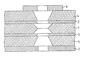
- the drawing schematically shows a section through a control plate constructed according to the invention perpendicular to the plate surfaces, a control hole being detected.
- 1 designates a metallic middle layer made of a NiFeCo alloy with a thickness of, for example, 80 ⁇ m.
- a glass solder layer 2 or 3 is connected on both sides of the layer surfaces.
- These layers 1 and 5 form the carrier plate of the control plate.
- On the outside of the glass layer 4 there is a metallic control electrode track 6, cut transversely to its longitudinal direction.
- a metallic control electrode track 7 is cut longitudinally. In the area of the control hole, all layers 1 to 5 of the carrier plate and the two control electrode tracks 6, 7 lie one above the other, the two control electrode tracks 6, 7 marking the matrix point as an overlap of the corresponding row and column.
- the control hole runs perpendicular to the control plate surfaces through all carrier plate layers 1 to 5 and through the control electrode tracks 6 and 7. It is produced, for example, by thermal etching.
- the carrier plate is produced beforehand as follows: the metal layer 1 is sprayed on both sides and the glass layers 4, 5 on one side with glass solder powder (e.g. Schott 8596). After the powder has dried, the layers 1, 4 and 5 are pressed together between two flat metal plates at a temperature of, for example, 520 ° C., which allows the glass solder powder to sinter together. This results in the glass solder layers 2 and 3, 5 hold together.
- the metallic control electrode tracks are then applied to the carrier plate. This is advantageously done galvanically by depositing metal layers on a photoresist mask onto a thin, previously vapor-deposited continuous contact layer.
- control holes are etched free in several steps.
- the control holes in the control electrode tracks 6, 7 have already been created by appropriate covering during galvanic deposition.
- a second masking leaves only the control points to be etched into the glass layers 4 and 5.
- the control holes through the glass layers 4, 5 to the glass solder layers 2, 3 are then formed by etching with dilute hydrofluoric acid.
- the glass solder layers 2, 3 are then etched with nitric acid solution, mixed with a little hydrofluoric acid, until the control holes expose the metal layer 1.
- the further etching of the control holes through the metal layer 1 takes place with an iron chloride solution, the glass solder layers 2 serving as a mask for this etching.
- This step etching causes relatively minor undercuts in the direction of the plate.
- the previously etched layer serves as a mask for the subsequent etching.
- control holes there are further possibilities to bring the control holes into the control plate by means of ion beam processes or laser beam processes.
- the laser beam process in particular allows precise drilling.
- the metallic middle layer 1 dissipates the heat generated during drilling, so that no local thermal stresses can arise in the glass layers 4, 5. There is no risk of cracking.
Landscapes
- Gas-Filled Discharge Tubes (AREA)
- Cathode-Ray Tubes And Fluorescent Screens For Display (AREA)
Claims (6)
Priority Applications (1)
| Application Number | Priority Date | Filing Date | Title |
|---|---|---|---|
| AT79103758T ATE101T1 (de) | 1978-10-12 | 1979-10-02 | Steuerplatte fuer einen flachen plasmabildschirm. |
Applications Claiming Priority (2)
| Application Number | Priority Date | Filing Date | Title |
|---|---|---|---|
| DE2844512A DE2844512C2 (de) | 1978-10-12 | 1978-10-12 | Steuerplatte zur Matrixansteuerung einzelner Bildpunkte nach Zeile und Spalte auf einem Bildschirm in flachen Plasmabildwiedergabevorrichtungen |
| DE2844512 | 1978-10-12 |
Publications (2)
| Publication Number | Publication Date |
|---|---|
| EP0010222A1 EP0010222A1 (fr) | 1980-04-30 |
| EP0010222B1 true EP0010222B1 (fr) | 1981-07-01 |
Family
ID=6052037
Family Applications (1)
| Application Number | Title | Priority Date | Filing Date |
|---|---|---|---|
| EP79103758A Expired EP0010222B1 (fr) | 1978-10-12 | 1979-10-02 | Plaque de commande pour un écran plat à plasma de reproduction d'image |
Country Status (5)
| Country | Link |
|---|---|
| US (1) | US4329617A (fr) |
| EP (1) | EP0010222B1 (fr) |
| JP (1) | JPS5578440A (fr) |
| AT (1) | ATE101T1 (fr) |
| DE (1) | DE2844512C2 (fr) |
Families Citing this family (7)
| Publication number | Priority date | Publication date | Assignee | Title |
|---|---|---|---|---|
| GB2154053A (en) * | 1984-02-08 | 1985-08-29 | Philips Electronic Associated | High resolution channel multiplier dynodes |
| US4504565A (en) * | 1984-04-17 | 1985-03-12 | Markem Corporation | Radiation imageable compositions containing hollow ceramic microspheres |
| EP0189858A3 (fr) * | 1985-01-31 | 1986-10-29 | Siemens Aktiengesellschaft | Unité de commande et son procédé de fabrication, en particulier pour dispositifs d'affichage |
| JPH0666130B2 (ja) * | 1985-04-25 | 1994-08-24 | 富士通株式会社 | ガス放電パネルの製造方法 |
| DE3609967A1 (de) * | 1986-03-25 | 1987-10-01 | Standard Elektrik Lorenz Ag | Steuerscheibe fuer bildwiedergabevorrichtungen |
| US5721468A (en) * | 1992-02-06 | 1998-02-24 | U.S. Philips Corporation | Flat-panel type picture display device with electron propagation ducts |
| US6956210B2 (en) * | 2003-10-15 | 2005-10-18 | Micron Tchnology, Inc. | Methods for preparing samples for atom probe analysis |
Family Cites Families (9)
| Publication number | Priority date | Publication date | Assignee | Title |
|---|---|---|---|---|
| US3755704A (en) * | 1970-02-06 | 1973-08-28 | Stanford Research Inst | Field emission cathode structures and devices utilizing such structures |
| US3753022A (en) * | 1971-04-26 | 1973-08-14 | Us Army | Miniature, directed, electron-beam source |
| US3744247A (en) * | 1971-09-14 | 1973-07-10 | Nasa | Single grid accelerator for an ion thrustor |
| US3777206A (en) * | 1972-03-24 | 1973-12-04 | Sperry Rand Corp | Electrodes for gas plasma display panels and method of manufacture thereof |
| JPH0127432B2 (fr) * | 1975-01-24 | 1989-05-29 | Hitachi Ltd | |
| NL7600419A (nl) * | 1976-01-16 | 1977-07-19 | Philips Nv | Kleurenbeeldbuis en werkwijze ter vervaardiging daarvan. |
| DE2615721C2 (de) * | 1976-04-09 | 1982-10-21 | Siemens AG, 1000 Berlin und 8000 München | Anzeigevorrichtung mit einem Gasentladungsraum als Quelle für Elektronen und einem Nachbeschleunigungsraum zur Nachbeschleunigung dieser Elektronen |
| DE2750587A1 (de) * | 1977-11-11 | 1979-05-17 | Siemens Ag | Gasentladungsanzeigevorrichtung mit abstandselementen |
| US4160191A (en) * | 1977-12-27 | 1979-07-03 | Hausfeld David A | Self-sustaining plasma discharge display device |
-
1978
- 1978-10-12 DE DE2844512A patent/DE2844512C2/de not_active Expired
-
1979
- 1979-10-02 EP EP79103758A patent/EP0010222B1/fr not_active Expired
- 1979-10-02 AT AT79103758T patent/ATE101T1/de not_active IP Right Cessation
- 1979-10-05 US US06/082,168 patent/US4329617A/en not_active Expired - Lifetime
- 1979-10-11 JP JP13128279A patent/JPS5578440A/ja active Pending
Also Published As
| Publication number | Publication date |
|---|---|
| DE2844512C2 (de) | 1980-11-20 |
| US4329617A (en) | 1982-05-11 |
| DE2844512B1 (de) | 1980-03-20 |
| JPS5578440A (en) | 1980-06-13 |
| ATE101T1 (de) | 1981-07-15 |
| EP0010222A1 (fr) | 1980-04-30 |
Similar Documents
| Publication | Publication Date | Title |
|---|---|---|
| DE3106368C2 (de) | Gleichstrom-Gasentladungsanzeigevorrichtung | |
| DE4341149C2 (de) | Multipolvorrichtung und Verfahren zum Herstellen einer Multipolvorrichtung | |
| EP0048839A1 (fr) | Ecran de visualisation plat, procédés pour sa fabrication et son utilisation | |
| EP0010222B1 (fr) | Plaque de commande pour un écran plat à plasma de reproduction d'image | |
| DE2700424A1 (de) | Farbbildroehre und verfahren zu deren herstellung | |
| DE2855142A1 (de) | Leuchtschirm fuer bildanzeigeroehren und verfahren zu seiner herstellung | |
| DE3200670C2 (fr) | ||
| EP0031921B1 (fr) | Dispositif d'affichage à décharge à gaz comportant au moins un cadre d'écartement limitant l'espace de post-accélération | |
| EP0142765A2 (fr) | Méthode pour la fabrication d'un dispositif d'affichage et dispositif d'affichage fabriqué selon cette méthode | |
| EP0662703B1 (fr) | Emetteur d'électrons thermo-ionique réglable | |
| DE69618177T2 (de) | Verfahren zur mechanischen und elektrischen verbindung eines substrates | |
| DE3408848C2 (de) | Verfahren zur Herstellung von Vielkanalplatten | |
| DE2063578A1 (de) | Verfahren zum Herstellen einer Maskenelektrode für eine Farbfernsehbildrohre mit verengten, vorlaufigen Offnungen | |
| DE2421512A1 (de) | Gasentladungs-anzeigetafel und verfahren zu ihrer herstellung | |
| DE2700141A1 (de) | Farbbildroehre und verfahren zu deren herstellung | |
| DE3036591A1 (de) | Gasentladungsbildwiedergabepaneel mit hohlen kathoden | |
| DE1218072B (de) | Sekundaerelektronenvervielfacher und Verfahren zur Herstellung des Vervielfachers | |
| DE2633619C2 (de) | Speicherplatte für eine Kathodenstrahlröhre und Verfahren zu deren Herstellung | |
| DE1941667A1 (de) | Anordnung zum Empfang von Bildsignalen und Synchronisiersignalen | |
| DE2615681C2 (de) | Anzeigevorrichtung mit einem Gasentladungsraum als Elektronenquelle, mit einem Elektronennachbeschleunigungsraum und mit einem Leuchtschirm | |
| EP0162135A2 (fr) | Dispositif d'affichage et méthode de fabrication | |
| DE3534030A1 (de) | Elektronensteuereinheit und verfahren zu deren herstellung, insbesondere fuer gasentladungsanzeigevorrichtungen | |
| DE2113198A1 (de) | Anzeigevorrichtung oder -tafel | |
| DE3411930A1 (de) | Verfahren zur herstellung einer steuerplatte fuer einen flachbildschirm, danach hergestellte steuerplatte und ihre verwendung | |
| DE2434455A1 (de) | Akustischer bildwandler |
Legal Events
| Date | Code | Title | Description |
|---|---|---|---|
| PUAI | Public reference made under article 153(3) epc to a published international application that has entered the european phase |
Free format text: ORIGINAL CODE: 0009012 |
|
| AK | Designated contracting states |
Designated state(s): AT CH FR GB IT NL SE |
|
| 17P | Request for examination filed | ||
| ITF | It: translation for a ep patent filed | ||
| GRAA | (expected) grant |
Free format text: ORIGINAL CODE: 0009210 |
|
| AK | Designated contracting states |
Designated state(s): AT CH FR GB IT NL SE |
|
| REF | Corresponds to: |
Ref document number: 101 Country of ref document: AT Date of ref document: 19810715 Kind code of ref document: T |
|
| PGFP | Annual fee paid to national office [announced via postgrant information from national office to epo] |
Ref country code: CH Payment date: 19831219 Year of fee payment: 5 |
|
| PGFP | Annual fee paid to national office [announced via postgrant information from national office to epo] |
Ref country code: SE Payment date: 19840930 Year of fee payment: 6 |
|
| PGFP | Annual fee paid to national office [announced via postgrant information from national office to epo] |
Ref country code: FR Payment date: 19841022 Year of fee payment: 6 |
|
| PGFP | Annual fee paid to national office [announced via postgrant information from national office to epo] |
Ref country code: AT Payment date: 19861003 Year of fee payment: 8 |
|
| PGFP | Annual fee paid to national office [announced via postgrant information from national office to epo] |
Ref country code: NL Payment date: 19861031 Year of fee payment: 8 |
|
| PG25 | Lapsed in a contracting state [announced via postgrant information from national office to epo] |
Ref country code: AT Effective date: 19871002 |
|
| PG25 | Lapsed in a contracting state [announced via postgrant information from national office to epo] |
Ref country code: SE Effective date: 19871003 |
|
| PG25 | Lapsed in a contracting state [announced via postgrant information from national office to epo] |
Ref country code: CH Effective date: 19871031 |
|
| PG25 | Lapsed in a contracting state [announced via postgrant information from national office to epo] |
Ref country code: NL Effective date: 19880501 |
|
| NLV4 | Nl: lapsed or anulled due to non-payment of the annual fee | ||
| GBPC | Gb: european patent ceased through non-payment of renewal fee | ||
| PG25 | Lapsed in a contracting state [announced via postgrant information from national office to epo] |
Ref country code: FR Free format text: LAPSE BECAUSE OF NON-PAYMENT OF DUE FEES Effective date: 19880630 |
|
| REG | Reference to a national code |
Ref country code: CH Ref legal event code: PL |
|
| REG | Reference to a national code |
Ref country code: FR Ref legal event code: ST |
|
| PG25 | Lapsed in a contracting state [announced via postgrant information from national office to epo] |
Ref country code: GB Effective date: 19881118 |
|
| PLBE | No opposition filed within time limit |
Free format text: ORIGINAL CODE: 0009261 |
|
| STAA | Information on the status of an ep patent application or granted ep patent |
Free format text: STATUS: NO OPPOSITION FILED WITHIN TIME LIMIT |