EP0154824A2 - Source d'ions - Google Patents
Source d'ions Download PDFInfo
- Publication number
- EP0154824A2 EP0154824A2 EP85101560A EP85101560A EP0154824A2 EP 0154824 A2 EP0154824 A2 EP 0154824A2 EP 85101560 A EP85101560 A EP 85101560A EP 85101560 A EP85101560 A EP 85101560A EP 0154824 A2 EP0154824 A2 EP 0154824A2
- Authority
- EP
- European Patent Office
- Prior art keywords
- gas
- ion source
- ion beam
- source according
- exit slit
- Prior art date
- Legal status (The legal status is an assumption and is not a legal conclusion. Google has not performed a legal analysis and makes no representation as to the accuracy of the status listed.)
- Granted
Links
Images


Classifications
-
- C—CHEMISTRY; METALLURGY
- C07—ORGANIC CHEMISTRY
- C07D—HETEROCYCLIC COMPOUNDS
- C07D401/00—Heterocyclic compounds containing two or more hetero rings, having nitrogen atoms as the only ring hetero atoms, at least one ring being a six-membered ring with only one nitrogen atom
- C07D401/02—Heterocyclic compounds containing two or more hetero rings, having nitrogen atoms as the only ring hetero atoms, at least one ring being a six-membered ring with only one nitrogen atom containing two hetero rings
-
- H—ELECTRICITY
- H01—ELECTRIC ELEMENTS
- H01J—ELECTRIC DISCHARGE TUBES OR DISCHARGE LAMPS
- H01J37/00—Discharge tubes with provision for introducing objects or material to be exposed to the discharge, e.g. for the purpose of examination or processing thereof
- H01J37/02—Details
- H01J37/04—Arrangements of electrodes and associated parts for generating or controlling the discharge, e.g. electron-optical arrangement or ion-optical arrangement
- H01J37/08—Ion sources; Ion guns
-
- H—ELECTRICITY
- H01—ELECTRIC ELEMENTS
- H01J—ELECTRIC DISCHARGE TUBES OR DISCHARGE LAMPS
- H01J27/00—Ion beam tubes
- H01J27/02—Ion sources; Ion guns
-
- H—ELECTRICITY
- H01—ELECTRIC ELEMENTS
- H01J—ELECTRIC DISCHARGE TUBES OR DISCHARGE LAMPS
- H01J27/00—Ion beam tubes
- H01J27/02—Ion sources; Ion guns
- H01J27/022—Details
-
- H—ELECTRICITY
- H01—ELECTRIC ELEMENTS
- H01J—ELECTRIC DISCHARGE TUBES OR DISCHARGE LAMPS
- H01J27/00—Ion beam tubes
- H01J27/02—Ion sources; Ion guns
- H01J27/16—Ion sources; Ion guns using high-frequency excitation, e.g. microwave excitation
- H01J27/18—Ion sources; Ion guns using high-frequency excitation, e.g. microwave excitation with an applied axial magnetic field
Definitions
- This invention relates to an ion source for an ion implanter, an ion milling machine or the like, and more particularly to an ion source suitable for obtaining a stable ion beam for an extended period of time, and further particularly to a microwave ion source suitable for obtaining a B ion beam.
- Figure 1 is a schematic illustration of the structure of a conventional microwave ion source.
- the microwave ion source consists of rectangular waveguides 2a and 2b as the waveguide for propagating a microwave, discharge electrodes 4 constituting a ridged waveguide structure, a discharge chamber 5 made of boron nitride and disposed between the ridged waveguides, and extraction electrodes 8a, 8b and 8c which extract the ion beam 21.
- An axial magnetic field generated by the excitation of a coil 13 is applied to the discharge chamber 5, and a feed gas for discharge is introduced into the discharge chamber 5 through a gas introduction pipe 6.
- Figure 2 shows in detail the discharge chamber and portions near the chamber.
- Figure 3 is a sectional view of the discharge chamber 5 and portions near the chamber, and is useful for explaining the discharge chamber 5, a gas inlet 10 and an ion beam exit slit 7.
- reference numeral 1 represents a - microwave generator; 3 is a microwave introducing flange; 5a is a lining of the discharge chamber 5; 7a is a portion near the ion beam exit slit; 11 is a dielectric filler; and 12 is an insulator.
- PH 3 (phosphine), AsH 3 (arsine) or the like as a hydride is used as the feed gas in order to obtain the beam of p + (phosphorus) ion, As + (arsenic) ion beam or the like that is used for the ion implantation for a semicondcutor in the ion source shown in Figure 1.
- the P + or As ion beam can be extracted stably for an extended period of time.
- a BF 3 gas is introduced in order to obtain B + ion beam necessary for the ion implantation for a semiconductor, however, two problems develop, which have made it difficult so far to obtain stably a high current ion beam for an extended period of time:
- the opening area is reduced so that the extracted beam current drops.
- the gas inlet 10 is positioned near the center of the discharge chamber 5. Therefore, if plasma is generated by a halide gas such as BF 3 , boron nitride (BN) constituting the lining 5a of the discharge chamber 5, partic- alarly its portion near the gas inlet 10, is etched, and an etching product (most of which is BN) precipitates at the other portions particularly at the ion beam exit slit 7. In consequence, the slit width is recuced, and the current drops eventually.
- a halide gas such as BF 3
- boron nitride (BN) constituting the lining 5a of the discharge chamber 5
- an etching product most of which is BN
- the area of the opening portion is reduced almost by half in the course of the operation of the ion source for about four hours.
- the deposit When the deposit is hit by the plasma or ion beam, it is peeled off from the ion beam exit slit 7 and flies sometimes into the space to which an electric field for extracting the ions is applied.
- the peeled matter strikes the electrode 8b and generates secondary electron emission, which in turn, generates an abnormal discharge between the electrode 8a to which a high positive voltage is applied and the electrode 8b to which a high negative voltage is applied. This results in unstability of the ion source.
- the deposit is often peeled off in the case of (2), too, and the plasma state becomes unstable, and, in addition, an abnormal discharge develops between the electrodes in the same way as in the case of (1), and reduces the stability of the ion source.
- the extracted ion beam current decreases and the stability of the ion source drops, as described above.
- the reason why the deposit occurs when the BF 3 or BCt3 gas is used is that since the fluorine or chlorine atom generated by microwave discharge is extremely active chemically, it corrodes and dissociates boron nitride (BN) that constitutes the lining 5a of the discharge chamber 5. As a matter of fact, when the deposit is physically analyzed, it is determined to be boron nitride. In order to prevent the occurrence of such a deposit, it is effective to constitute the discharge chamber in a thermally isolated structure, and to raise its operation temperature so as to thermally dissociate or evaporate the deposit.
- boron nitride boron nitride
- the temperature can not be raised beyond a certain limit due to the structural liminations of the discharge chamber (generally, the approximate upper limit is 800 to 900°C), and it has been difficult in practice in the past to restrict the quantity of deposit to a level which presents no practical problems.
- the present invention is directed to provide an ion source, particularly a microwave ion source, which can eliminate the problems with the prior art described above, which does not reduce the width of an ion beam exit slit even when a halide gas such as BF 3 or BCl 3 is used as a feed gas to be introduced into a discharge chamber, and makes it possible to stably extract an intended ion beam for an extended period of time.
- a halide gas such as BF 3 or BCl 3
- the ion source in accordance with the present invention is equipped with an gas,inlet in the proximity of an ion beam exit slit for extracting ions from the plasma of the feed gas introduced into a discharge chamber.
- the effect of the present invention can be further enhanced by using, as the feed gas to be introduced into the discharge chamber, a mixed gas prepared by mixing at least one gas selected from the above-mentioned boron halide gases with at least one gas, which reacts with boron to form a boron compound, such as oxygen, hydrogen or oxygen-containing compound gas.
- d is the distance between the gas inlet and the end surface of the discharge chamber on which the ion exit slit is disposed
- d should be up to 2d' and preferably, is up to d', which is the distance between the wall of the protion of the discharge chamber at which the gas inlet is disposed and the wall opposing the former, and if the gas inlet is positioned closer to the ion beam exit slit,a better result can be obtained.
- the gas pressure is elevated in the proximity of the ion beam exit slit, and the portion of the exit slit is etched in the same way as the walls inside the discharge chamber, thereby making it possible to reduce the deposit onto the exit slit portion.
- the quantity of the gas which reacts with boron to form a boron compound and which is to be mixed with the halide gas is at least 0.1% of the halide gas in a pressure ratio, and the effect of the invention increases remarkably as reactive gas quantity increases. If the gas quantity is below 0.1%, the effect of the invention can not be observed. If the quantity of the mixing gas such as oxygen increases, the quantity ⁇ of the intended ions contained in the extracted ion beam decreases in proportion to the mixing quantity, so that the upper limit of the mixing gas is determined in accordance with the object of use of the ion source. When the mixing gas is hydrogen, its mixing quantity is the same as the oxygen described above.
- the mixing gas may be any one of the above-mentioned gases of hydrogen, oxygen and various compounds containing oxygen, but two or more of these gases may be mixed and be used as the mixing gas. Addition of the mixing gas such as oxygen to the gas to be introduced into the discharge chamber provides naturally the effect of the invention in combination with disposition of the gas inlet in the proximity of the ion beam exit slit, but when it is used alone, addition of the mixing gas stabilizes ion beam extraction.
- Microwaves in a magnetic field are generally used as plasma generation means, and can also be used for the ion source of the present invention.
- the field of utilization of the plasma generated by microwave discharge in the magnetic field includes etching of Si by plasma. It is generally known that the etching rate drops due to the mixture of oxygen depending on the microwave plasma etching. It is known that when the B + beam is extracted by introducing BF 3 into the microwave ion source, relatively great quantities of ions of oxygen-containing compounds such as BO + , BOF or the like are detected as being generated if H 2 0 as the residual gas inside a vacuum chamber is great.
- an ion source for obtaining B + ion beam of a mA class an ion source utilizing low voltage arc discharge with a hot filmaent is known.
- BF 3 is also used for such an ion source. Since the hot filament is rapidly corroded by oxygen, operation of the ion source for an extended period can not be expected even if oxygen (0 2 ) is introduced in order to obtain a stable B + beam. In this sense, introduction of 0 2 is a method which can be characterizingly used for a microwave ion source not containing a hot filament.
- oxygen is used as a typical example, but the effect of reduction of deposition can be obtained with those gases which react with boron and which readily form a boron compound, such as H 2 gas.
- Figures 4 and 5 are sectional views, each showing the structure of a discharge chamber and portions nearby in a microwave ion source in accordance with a first embodiment of the present invention
- Figure 5 is a sectional view taken along line A - A in Figure 4.
- This embodiment uses microwave discharge in a magnetic field as means for generating plasma.
- the microwave is introduced into the discharge chamber 5 from the left side of Figure 4 through the space between the discharge electrodes 4.
- the magnetic field is applied in a direction crossing an electric field by the microwave, and the interaction of these fields generate the plasma of the feed gas inside the discharge chamber 5.
- Ion beam 21 is extracted from an ion beam exit slit 7 which is disposed on one end surface of the discharge chamber.
- the feed gas is introduced into the discharge chamber 5 through a plurality of gas inlets 110 (five inlets are shown in Figure 5) that are disposed in the proximity of the ion beam exit slit.
- the distance d between these gas inlets 110 and the end surface 120 of the discharge chamber, on which the exit slit 7 is disposed should be smaller than 2d', and is preferably smaller than d', which is the distance between the wall surface, on which the gas inlets are disposed, and the wall surface of the discharge chamber 5 facing the former.
- a hlide gas such as BF 3
- the deposit to the ion beam exit slit 7 can be reduced because the inner walls of the discharge chamber 5 close to the gas inlets 110 and the surface exposed to the plasma at the ion beam exit slit 7 are also etched.
- the diameter of the gas inlet 110 is 2 mm
- the length of the ion beam exit slit 7 is substantially the same as that of the discharge chamber
- the thickness of the slit 7 is about 1 mm
- the discharge chamber 5 is 8 mm wide, 20 mm deep and 46 mm long.
- the same material is used for each portion as in the prior art device. That is, the discharge electrode 4 is made of stainless steel, the dielectric filler 11 is made of BN, the lining 5a of the discharge chmaber is made of BN, and carbon is used for the portion 7a in the proximity of the ion beam exit slit 7.
- Figure 6 is a schematic illustration showing the overall structure of the microwave ion source of this embodiment.
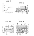
- Figure 7 is a diagram showing the relation between the position of the gas inlets 110 and the deposition quantity of the deposit at the ion beam exit slit.
- the abscissa represents d/d' ratio (R) wherein d' is the distance between the gas inlet and the inner wall of the discharge chamber facing the gas inlet and d is the distance between the end surface of the discharge cahmber on which the ion beam exit slit is disposed and the gas inlet, and the ordinate represents the deposition rate (mm/hr).
- the ion beam exit slit and the discharge chamber have the same structure as described already.
- the microwave power to be charged into the plasma is 800 W
- the intensity of magnetic field is 500 Gauss
- the feed gas quantity expressed in terms of pressure is 1x10 -1 Pa, and these values are kept constant.
- a negative deposition rate indicates that the ion beam exit slit has been etched.
- undesirable deposition occurs greatly in the region where R > 2.
- R the value of the present invention
- the smaller the value R the smaller the deposition quantity.
- the operating life enough for the practical use as an ion source for ion implanter can be obtained.
- (implant current) x (implant time) 40 mA. hr can be achieved.
- FIGS 8a and 8b are sectional and plan views showing a discharge chamber and portions nearby in a microwave ion source in accordance with a second embodiment of the present invention.
- the feed gas is introduced into the discharge chamber in the same way as in the first embodiment shown in Figure 4.
- the ion beam exit slit is divided into a plurality of units in a thermally isolated state so that the temperature of the portions of the ion beam exit slit 7, which are exposed to plasma, can be further raised.
- the ion beam exit slit 7 in this embodiment consists of three members 7a, 7b and 7c, whereby 7a is made of stainless steel, 7b is made of an electrically conductive composite material of electrically conductive BN and Ti, and 7c is made of carbon.
- the ion beam exit slit 7 is thermally isolated and consists of a plurality of units as shown in Figure 8 b .
- This split structure raises the temperature of BN by thermally isolating the slit 7, and makes the slit 7 more readily etchable when the discharge gas passes therethrough.
- This embodiment can further enhance the etching effect of. the ion beam exit slit 7 by the feed gas, and can eliminate the deposit on the ion beam exit slit 7.
- FIG 9 is a sectional view showing the structure of the discharge chamber of the microwave ion source and portions nearby in accordance with a third embodiment of the present invention.
- the feed gas is introduced into the discharge chamber through the gas inlet 110 disposed close to the ion beam exit slit 7 and through a gas inlet 110a which is additionally disposed on the surface at the depth of the discharge chamber 5 (on the surface on the left hand of Figure 9).
- the gas introduction pipes 6 and 6a communicating with these two gas inlets 110 and 110a have separate gas flow rate control valves 9a and 9b, respectively, and can independently control the gas flow rate.
- This embodiment can uniformly reduce the deposit inside the discharge chamber 5 by adjusting the respective gas flow rates to match the state of deposit at the ion beam exit slit 7 and on the deep surface of the discharge chamber 5.
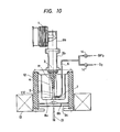
- This embodiment is the same as the ion source shown in the first embodiment except that leak valves 14 and 14 4 are fitted to the gas introduction pipe 6 as shown in Figure 10, and a gas mixture, boron trifluoride (BF 3 ) and oxygen (0 2 ),_is introduced.
- boron trifluoride BF 3
- oxygen 0 2
- the microwave ion source in accordance with a fifth embodiment of the invention is the same as the ion source of the fourth embodiment except that BF 3 and 0 2 are introduced into the discharge chamber 5 through separate gas introduction pipes 6 and 6', as shown in Figure 11.
- a stable B + beam free from deposition can be obtained in this embodiment in the same way as in the fourth embodiment shown in Figure 10.
- Reference numerals 15 and 15' in Figure 11 represent the leak valves, respectively.
- the mixed gas can be introduced into the discharge chamber through one needle valve as shown in Figure 6, and the same effect as those of the fourth and fifth embodiments can be obtained.
- a stable B + beam can be extracted without causing any deposition.
- the present invention can prevent the deposition on the ion beam exit slit, and hence can extract ions stably for an extended period of time.
- a B + ion beam of at least 4 mA which has not so far been accomplished by the prior art ion source, can now be obtained for 4 or more. hours stably.
- an ion implant current of a semiconductor ion implanter on a production line remains at about 2 mA at present,-the present invention makes it possible for the first time to carry out high current B + ion implantation at a practical level, and provides a great effect in practice.
Landscapes
- Chemical & Material Sciences (AREA)
- Engineering & Computer Science (AREA)
- Combustion & Propulsion (AREA)
- Organic Chemistry (AREA)
- Analytical Chemistry (AREA)
- Electron Sources, Ion Sources (AREA)
Applications Claiming Priority (4)
| Application Number | Priority Date | Filing Date | Title |
|---|---|---|---|
| JP59049064A JPS60195853A (ja) | 1984-03-16 | 1984-03-16 | マイクロ波イオン源 |
| JP59049065A JPH0622107B2 (ja) | 1984-03-16 | 1984-03-16 | イオン源 |
| JP49065/84 | 1984-03-16 | ||
| JP49064/84 | 1984-03-16 |
Publications (3)
| Publication Number | Publication Date |
|---|---|
| EP0154824A2 true EP0154824A2 (fr) | 1985-09-18 |
| EP0154824A3 EP0154824A3 (en) | 1987-04-29 |
| EP0154824B1 EP0154824B1 (fr) | 1991-09-18 |
Family
ID=26389412
Family Applications (1)
| Application Number | Title | Priority Date | Filing Date |
|---|---|---|---|
| EP85101560A Expired - Lifetime EP0154824B1 (fr) | 1984-03-16 | 1985-02-13 | Source d'ions |
Country Status (4)
| Country | Link |
|---|---|
| US (1) | US4658143A (fr) |
| EP (1) | EP0154824B1 (fr) |
| KR (1) | KR920003156B1 (fr) |
| DE (1) | DE3584105D1 (fr) |
Cited By (3)
| Publication number | Priority date | Publication date | Assignee | Title |
|---|---|---|---|---|
| EP0360932A1 (fr) * | 1988-09-28 | 1990-04-04 | Norman A. Bostrom | Source d'ions à micro-ondes |
| GB2230644A (en) * | 1989-02-16 | 1990-10-24 | Tokyo Electron Ltd | Electron beam excitation ion source |
| EP0703597A1 (fr) * | 1994-09-26 | 1996-03-27 | Eaton Corporation | Source d'ion à micro-ondes pour l'implantation ionique |
Families Citing this family (24)
| Publication number | Priority date | Publication date | Assignee | Title |
|---|---|---|---|---|
| JPH0616384B2 (ja) * | 1984-06-11 | 1994-03-02 | 日本電信電話株式会社 | マイクロ波イオン源 |
| JP2530434B2 (ja) * | 1986-08-13 | 1996-09-04 | 日本テキサス・インスツルメンツ株式会社 | イオン発生装置 |
| YU46728B (sh) * | 1986-10-23 | 1994-04-05 | VUJO dr. MILJEVIĆ | Jonsko-elektronski izvor sa šupljom anodom |
| US4797597A (en) * | 1986-12-22 | 1989-01-10 | Bostrom Norman A | Microwave ion source |
| US5053678A (en) * | 1988-03-16 | 1991-10-01 | Hitachi, Ltd. | Microwave ion source |
| US5089746A (en) * | 1989-02-14 | 1992-02-18 | Varian Associates, Inc. | Production of ion beams by chemically enhanced sputtering of solids |
| JP2700280B2 (ja) * | 1991-03-28 | 1998-01-19 | 理化学研究所 | イオンビーム発生装置および成膜装置および成膜方法 |
| US5206516A (en) * | 1991-04-29 | 1993-04-27 | International Business Machines Corporation | Low energy, steered ion beam deposition system having high current at low pressure |
| US5196706A (en) * | 1991-07-30 | 1993-03-23 | International Business Machines Corporation | Extractor and deceleration lens for ion beam deposition apparatus |
| US5914494A (en) * | 1996-03-27 | 1999-06-22 | Thermoceramix, Llc | Arc chamber for an ion implantation system |
| US6022258A (en) * | 1996-03-27 | 2000-02-08 | Thermoceramix, Llc | ARC chamber for an ion implantation system |
| US6239440B1 (en) | 1996-03-27 | 2001-05-29 | Thermoceramix, L.L.C. | Arc chamber for an ion implantation system |
| US5857889A (en) * | 1996-03-27 | 1999-01-12 | Thermoceramix, Llc | Arc Chamber for an ion implantation system |
| US6355933B1 (en) * | 1999-01-13 | 2002-03-12 | Advanced Micro Devices, Inc. | Ion source and method for using same |
| US6627901B2 (en) | 2001-01-04 | 2003-09-30 | Nec Electronics, Inc. | Apparatus and method for distribution of dopant gases or vapors in an arc chamber for use in an ionization source |
| RU2229754C2 (ru) * | 2002-07-16 | 2004-05-27 | Институт электрофизики Уральского отделения РАН | Плазменный эмиттер ионов |
| US7122966B2 (en) * | 2004-12-16 | 2006-10-17 | General Electric Company | Ion source apparatus and method |
| KR101103410B1 (ko) * | 2009-09-22 | 2012-01-05 | 엑스퍼트(주) | 이온생성챔버 |
| TWI466179B (zh) | 2010-02-26 | 2014-12-21 | 尖端科技材料股份有限公司 | 用以增進離子植入系統中之離子源的壽命及性能之方法與設備 |
| US8779383B2 (en) | 2010-02-26 | 2014-07-15 | Advanced Technology Materials, Inc. | Enriched silicon precursor compositions and apparatus and processes for utilizing same |
| US8686379B1 (en) | 2010-09-07 | 2014-04-01 | Joseph C. Robinson | Method and apparatus for preparing serial planar cross sections |
| US8878147B2 (en) | 2010-09-07 | 2014-11-04 | Joseph C. Robinson | Method and apparatus for in situ preparation of serial planar surfaces for microscopy |
| SG11201601015RA (en) | 2013-08-16 | 2016-03-30 | Entegris Inc | Silicon implantation in substrates and provision of silicon precursor compositions therefor |
| US11768176B2 (en) | 2022-01-06 | 2023-09-26 | Mks Instruments, Inc. | Ion source with gas delivery for high-fidelity analysis |
Family Cites Families (9)
| Publication number | Priority date | Publication date | Assignee | Title |
|---|---|---|---|---|
| DE2408829C2 (de) * | 1974-02-23 | 1984-03-22 | Ibm Deutschland Gmbh, 7000 Stuttgart | Bor-Ionenquell-Material und Verfahren zu seiner Herstellung |
| US4058748A (en) * | 1976-05-13 | 1977-11-15 | Hitachi, Ltd. | Microwave discharge ion source |
| US4175234A (en) * | 1977-08-05 | 1979-11-20 | University Of Virginia | Apparatus for producing ions of thermally labile or nonvolatile solids |
| US4139772A (en) * | 1977-08-08 | 1979-02-13 | Western Electric Co., Inc. | Plasma discharge ion source |
| JPS5852297B2 (ja) * | 1979-06-04 | 1983-11-21 | 株式会社日立製作所 | マイクロ波イオン源 |
| US4318028A (en) * | 1979-07-20 | 1982-03-02 | Phrasor Scientific, Inc. | Ion generator |
| US4393333A (en) * | 1979-12-10 | 1983-07-12 | Hitachi, Ltd. | Microwave plasma ion source |
| US4447773A (en) * | 1981-06-22 | 1984-05-08 | California Institute Of Technology | Ion beam accelerator system |
| JPS5923432A (ja) * | 1982-07-30 | 1984-02-06 | Hitachi Ltd | プラズマイオン源 |
-
1985
- 1985-02-13 EP EP85101560A patent/EP0154824B1/fr not_active Expired - Lifetime
- 1985-02-13 DE DE8585101560T patent/DE3584105D1/de not_active Expired - Lifetime
- 1985-02-21 KR KR1019850001084A patent/KR920003156B1/ko not_active Expired
- 1985-03-14 US US06/711,824 patent/US4658143A/en not_active Expired - Lifetime
Cited By (5)
| Publication number | Priority date | Publication date | Assignee | Title |
|---|---|---|---|---|
| EP0360932A1 (fr) * | 1988-09-28 | 1990-04-04 | Norman A. Bostrom | Source d'ions à micro-ondes |
| GB2230644A (en) * | 1989-02-16 | 1990-10-24 | Tokyo Electron Ltd | Electron beam excitation ion source |
| US5089747A (en) * | 1989-02-16 | 1992-02-18 | Tokyo Electron Limited | Electron beam excitation ion source |
| GB2230644B (en) * | 1989-02-16 | 1994-03-23 | Tokyo Electron Ltd | Electron beam excitation ion source |
| EP0703597A1 (fr) * | 1994-09-26 | 1996-03-27 | Eaton Corporation | Source d'ion à micro-ondes pour l'implantation ionique |
Also Published As
| Publication number | Publication date |
|---|---|
| EP0154824A3 (en) | 1987-04-29 |
| EP0154824B1 (fr) | 1991-09-18 |
| US4658143A (en) | 1987-04-14 |
| KR850006965A (ko) | 1985-10-25 |
| KR920003156B1 (ko) | 1992-04-20 |
| DE3584105D1 (de) | 1991-10-24 |
Similar Documents
| Publication | Publication Date | Title |
|---|---|---|
| US4658143A (en) | Ion source | |
| US5977552A (en) | Boron ion sources for ion implantation apparatus | |
| US7259378B2 (en) | Closed drift ion source | |
| US5900284A (en) | Plasma generating device and method | |
| EP0283519B1 (fr) | Generateur ionique, installation de formation de films minces utilisant ce generateur et source d'ions | |
| Kaufman et al. | Ion source design for industrial applications | |
| DE68924413T2 (de) | Radiofrequenzinduktion/Mehrpolplasma-Bearbeitungsvorrichtung. | |
| CN1210750C (zh) | 用于离子源的磁性过滤器 | |
| Gavrilov et al. | Development of technological sources of gas ions on the basis of hollow-cathode glow discharges | |
| EP0476900B1 (fr) | Appareil et procédé utilisant un plasma produit par micro-onde | |
| US4496843A (en) | Method for producing metal ions | |
| US4749910A (en) | Electron beam-excited ion beam source | |
| JPH0572053B2 (fr) | ||
| EP0215618A2 (fr) | Sources d'ions | |
| Keller et al. | Metal beam production using a high current ion source | |
| US4540868A (en) | Plasma gun that reduces cathode contamination | |
| US6055929A (en) | Magnetron | |
| Walther et al. | Production of atomic or molecular nitrogen ion beams using a multicusp and a microwave ion source | |
| Ehlers et al. | Increasing the efficiency of a multicusp ion source | |
| Flemming | Penning source for ion implantation | |
| RU2248064C1 (ru) | Источник ионов | |
| JPH0622107B2 (ja) | イオン源 | |
| Sampayan et al. | An improved ion source for ion implantation | |
| Aitken | Ion sources | |
| Drummond | Small electron and ion beams in surface analysis: their optics, interactions and uses |
Legal Events
| Date | Code | Title | Description |
|---|---|---|---|
| PUAI | Public reference made under article 153(3) epc to a published international application that has entered the european phase |
Free format text: ORIGINAL CODE: 0009012 |
|
| 17P | Request for examination filed |
Effective date: 19850213 |
|
| AK | Designated contracting states |
Designated state(s): DE FR GB |
|
| PUAL | Search report despatched |
Free format text: ORIGINAL CODE: 0009013 |
|
| AK | Designated contracting states |
Kind code of ref document: A3 Designated state(s): DE FR GB |
|
| 17Q | First examination report despatched |
Effective date: 19880419 |
|
| GRAA | (expected) grant |
Free format text: ORIGINAL CODE: 0009210 |
|
| AK | Designated contracting states |
Kind code of ref document: B1 Designated state(s): DE FR GB |
|
| REF | Corresponds to: |
Ref document number: 3584105 Country of ref document: DE Date of ref document: 19911024 |
|
| ET | Fr: translation filed | ||
| PLBE | No opposition filed within time limit |
Free format text: ORIGINAL CODE: 0009261 |
|
| STAA | Information on the status of an ep patent application or granted ep patent |
Free format text: STATUS: NO OPPOSITION FILED WITHIN TIME LIMIT |
|
| 26N | No opposition filed | ||
| REG | Reference to a national code |
Ref country code: GB Ref legal event code: IF02 |
|
| PGFP | Annual fee paid to national office [announced via postgrant information from national office to epo] |
Ref country code: FR Payment date: 20040122 Year of fee payment: 20 |
|
| PGFP | Annual fee paid to national office [announced via postgrant information from national office to epo] |
Ref country code: GB Payment date: 20040202 Year of fee payment: 20 |
|
| PGFP | Annual fee paid to national office [announced via postgrant information from national office to epo] |
Ref country code: DE Payment date: 20040304 Year of fee payment: 20 |
|
| PG25 | Lapsed in a contracting state [announced via postgrant information from national office to epo] |
Ref country code: GB Free format text: LAPSE BECAUSE OF EXPIRATION OF PROTECTION Effective date: 20050212 |
|
| REG | Reference to a national code |
Ref country code: GB Ref legal event code: PE20 |