EP0155370A2 - Circuit d'adressage de mémoire - Google Patents
Circuit d'adressage de mémoire Download PDFInfo
- Publication number
- EP0155370A2 EP0155370A2 EP84114786A EP84114786A EP0155370A2 EP 0155370 A2 EP0155370 A2 EP 0155370A2 EP 84114786 A EP84114786 A EP 84114786A EP 84114786 A EP84114786 A EP 84114786A EP 0155370 A2 EP0155370 A2 EP 0155370A2
- Authority
- EP
- European Patent Office
- Prior art keywords
- address
- register
- output
- input
- circuit
- Prior art date
- Legal status (The legal status is an assumption and is not a legal conclusion. Google has not performed a legal analysis and makes no representation as to the accuracy of the status listed.)
- Granted
Links
Images

Classifications
-
- G—PHYSICS
- G06—COMPUTING OR CALCULATING; COUNTING
- G06F—ELECTRIC DIGITAL DATA PROCESSING
- G06F5/00—Methods or arrangements for data conversion without changing the order or content of the data handled
- G06F5/06—Methods or arrangements for data conversion without changing the order or content of the data handled for changing the speed of data flow, i.e. speed regularising or timing, e.g. delay lines, FIFO buffers; over- or underrun control therefor
- G06F5/10—Methods or arrangements for data conversion without changing the order or content of the data handled for changing the speed of data flow, i.e. speed regularising or timing, e.g. delay lines, FIFO buffers; over- or underrun control therefor having a sequence of storage locations each being individually accessible for both enqueue and dequeue operations, e.g. using random access memory
-
- G—PHYSICS
- G06—COMPUTING OR CALCULATING; COUNTING
- G06F—ELECTRIC DIGITAL DATA PROCESSING
- G06F12/00—Accessing, addressing or allocating within memory systems or architectures
- G06F12/02—Addressing or allocation; Relocation
- G06F12/0215—Addressing or allocation; Relocation with look ahead addressing means
-
- G—PHYSICS
- G11—INFORMATION STORAGE
- G11C—STATIC STORES
- G11C8/00—Arrangements for selecting an address in a digital store
- G11C8/04—Arrangements for selecting an address in a digital store using a sequential addressing device, e.g. shift register, counter
-
- G—PHYSICS
- G06—COMPUTING OR CALCULATING; COUNTING
- G06F—ELECTRIC DIGITAL DATA PROCESSING
- G06F2205/00—Indexing scheme relating to group G06F5/00; Methods or arrangements for data conversion without changing the order or content of the data handled
- G06F2205/06—Indexing scheme relating to groups G06F5/06 - G06F5/16
- G06F2205/063—Dynamically variable buffer size
Definitions
- the invention relates to a circuit for addressing a memory via an address register.
- the circuit forms a sequence of addresses which, in particular starting from an address area lower limit, traverses the address area in individual steps in the ascending direction, switching over to the address area lower limit each time an address area upper limit is reached, and a further one, the address area gradually in ascending direction continuous address sequence is given.
- cyclic addressing can also be understood to mean that the circuit forms a sequence of addresses which, in particular starting from an upper address area limit, passes through the address area step by step in a descending direction, switching to the upper address area limit after reaching the lower address area limit and with a further one , the address range is continued in the descending direction.
- the advantage that can be achieved with the invention is, in particular, that the cyclic memory addressing allows the data stored in a plurality of memory locations to be periodically queried in a simple manner and processed or compared with other data, the limits of the address area and thus the limits of the queried memory area are arbitrarily definable.
- the cyclic memory addressing allows signal processing to be carried out in a particularly advantageous manner, the data stored in the periodically queried memory locations corresponding to the successively sampled function values of a time-dependent signal to be processed. It is possible to store a predetermined number of such samples with a minimum of re-storage processes and to change the inventory of the stored samples with each new sample in such a way that it replaces the oldest stored sample. This means that the stored inventory of samples is updated step by step. Cyclic memory addressing allows the stored, updated data to be read out in a very simple manner for further processing.
- Claims 3 to 5 are directed to preferred refinements and developments of the invention.
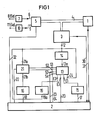
- a data processing system with an arithmetic unit 1, a tail unit 2 and a memory with random access (RAM) 3 is shown.
- the arithmetic logic unit 1 is connected via a bus 4 to the memory 3 and to an input / output unit 5, the input of which is connected to an analog / digital converter 7 via an n-wire line 6. Its input 8 is assigned a time-dependent analog signal Se to be processed.
- An output of 5 is connected via an n-wire line 9 to a digital / analog converter 10, at the output 11 of which an analog signal Sa can be tapped.
- 13 denotes an address multiplexer, the output 13a of which is connected to an address register 14.
- the output of 14 is connected to the address input 12 of the memory 3.
- a register 15 for storing an address area lower limit and a register 16 for storing an address area upper limit are provided, the inputs of which are each connected to the tail unit 2 via line bundles 17 and 18.
- An incrementing device 19 is connected via its input 19a to the output of the address register 14.
- the outputs of the register 15 and the incrementing device 19 are connected to the inputs E1 and E2 of the address multiplexer 13.
- An n-wire address input line 20 connects the tail 2 to the input E3 of 13.
- the output of the address register 14 is connected to the input E4 of 13.
- the outputs of the address register 14 and the register 16 are to inputs 21a and 21b of a logic circuit 21 which is controlled by the tail unit 2 via the line 22.
- Two outputs of the logic circuit 21 are connected to two control inputs S1 and S2 of the address multiplexer 13, while two further control inputs S3 and S4 of 13 are connected to the tail unit 2 via lines 23 and 24.
- the logic circuit 21 operates in such a way that, if the contents of the address register 14 and the register 16 are identical, a control signal is transmitted via the one output to S1 as a function of a command signal on the line 22. If these register contents are not identical, a control signal is transmitted to S2 via the other output as a function of a command signal on line 22.
- register 15 is input an n-digit binary number via line bundle 17, which represents the lower limit of the address area. Another n-digit binary number is entered into register 16 via line bundle 18, which means the upper limit of the address area. If you now enter an additional n-digit binary number between these two binary numbers via the address input line 20 and switch this through a command signal on line 23 via E3 to the output 13a of the address multiplexer 13, this binary number is set to Transfer address register 14. An address is thus output via the output from 14 to the address input 12 which lies within the set address range.
- next command signal on line 22 causes logic circuit 21 to emit a signal at input S1 of FIG.
- the next following command signals on line 22 then again cause the delivery of an address sequence which passes through the address area step by step in the ascending direction.
- the incrementing device 19 expediently consists of a binary counter which, when a binary number is input via the input 19a, automatically by a certain increment, e.g. 1, increased binary number to the input E2 of the address multiplexer 13.
- FIG. 2 A preferred circuit design of the logic circuit 21 is shown in FIG. 2.
- the (n-pole) inputs 21a and 21b of 21 at the same time represent the inputs of an exclusive OR circuit 25, the (n-pole) output of which is led to the n inputs of an OR circuit 26.
- the output of the latter is connected, on the one hand, via an inverter 27 to the first input of an AND gate 28 and, on the other hand, to the first input of an AND gate 29.
- the second inputs of the AND gates 28 and 29 are connected to the control line 22.
- the output of the AND gate 28 is connected to the control input S1 of the address multiplexer 13, while the output of the AND gate 29 is connected to S2 of 13.
- a logical "1" is always present at the output of the OR circuit 26 when the n-digit binary numbers supplied via 21a and 21b differ from one another. However, this means that the AND gate 28 is blocked, while the 3 error signals arriving on line 18 are transmitted to S2 via the AND gate 29 and cause an incremental forwarding of the respectively output addresses. If the register contents of 14 and 16 are the same, the same binary numbers are supplied via 21a and 215. In this case, a logic "0" appears at the output of 26, the AND gate 28 transmitting the next command signal on line 22 to the control input of S1, while the AND gate 29 blocks.
- incrementing device 19 in FIG. 1 is replaced by a decrementing device which consists, for example, of a down counter, and at the same time the register 15 is used for storing the upper limit of the address area and the register 16 for storing the lower limit of the address area, this results in a cyclical addressing, in which the between them Address range lying within boundaries is traversed by the individual address sequences in the descending direction.
- Command signals are transmitted to the memory 3 from the tail unit 2 via control lines 30, which signals it e.g. cause either to write a binary number received via the bus 4 into a memory location addressed via the address register 14 or to read a binary number stored in a memory location addressed via the address register 14 onto the bus 4.
- Control lines 31 are used to transmit commands, e.g. Operation commands, between the tail unit 2 and the arithmetic unit 1, while control lines 32 are used to switch through the line 6 in the input / output unit 5 in the direction of the collecting line 4 or the collecting line 4 in the direction of the line 9.
- a method for operating the data processing system according to FIG. 1 is described below, which uses cyclical addressing of an area of the memory 3 in order to provide samples of the analog, time-dependent signal Se present at 8 for processing in the arithmetic logic unit 1.
- the signal Se is periodically sampled by the analog / digital converter 7, a sequence of digital sampled values being formed, each of which consists of n-digit binary numbers Y1, Y2 ... etc.
- a predetermined number of these samples is successively transferred to the collecting line 4 via the input / output unit 5 and from there to the memory 3, where they are written into a corresponding number of memory locations.
- the latter are addressed in succession via the address register 14.
- FIG. 3 the memory locations P1 ...? 5 by a correspondingly divided block 33 shown.
- Addressing P1 ... P5 synchronously with the occurrence of the individual sample values Y1 ... Y5 takes place by means of an address sequence given by 14 with the individual addresses Z1 ... Z5, which is shown in FIG. 3 by the pointers Z1 ... Z5 are illustrated.
- the sample value Y1 is stored in P1, the sample value Y2 in P2, etc.
- the address sequence Z1 to Z5 is expediently generated in such a way that Z1 is entered via the address input line 20 as the start address and by a Signal on line 23 is switched through to the output of address register 14.
- the lines 30 are assigned the "write-in” command during the delivery of this address, so that the sample Y1 stored at the address Z1, which represents the oldest of the stored samples, is replaced or overwritten by a new sample Y6. If the remaining addresses Z22 to Z52 occur within the second pass, the "read" command is given on line 30.
- the sample values Y1 to Y5 are read out in a first readout period, the values Y2 ... Y6 in a second readout period, the sample values Y3 ... Y7 etc. in a third readout period, so that an inventory of updated from readout period to readout period Samples of the further processing is used.
- the addresses Z1, Z2 ... Z5, Z12, Z23, Z34, Z45 and Z56 are output at the same time intervals.
- the result values obtained which take into account, for example, filtering of the temporal signal Se in a transversal filter with predetermined filter coefficients, are sent via the bus 4 and the correspondingly controlled input / output unit 5 is output on line 9.
- the digital / analog converter i0 derives analog values from the incoming digital result values which, in their entirety, in particular after further filtering in a downstream low-pass filter, represent the analog output signal Sa.
Landscapes
- Engineering & Computer Science (AREA)
- Theoretical Computer Science (AREA)
- Physics & Mathematics (AREA)
- General Engineering & Computer Science (AREA)
- General Physics & Mathematics (AREA)
- Microelectronics & Electronic Packaging (AREA)
- Complex Calculations (AREA)
- Static Random-Access Memory (AREA)
- Techniques For Improving Reliability Of Storages (AREA)
- Storage Device Security (AREA)
Priority Applications (1)
| Application Number | Priority Date | Filing Date | Title |
|---|---|---|---|
| AT84114786T ATE71229T1 (de) | 1984-03-16 | 1984-12-05 | Schaltung zur adressierung eines speichers. |
Applications Claiming Priority (2)
| Application Number | Priority Date | Filing Date | Title |
|---|---|---|---|
| DE19843409751 DE3409751A1 (de) | 1984-03-16 | 1984-03-16 | Schaltung zur adressierung eines speichers |
| DE3409751 | 1984-03-16 |
Publications (3)
| Publication Number | Publication Date |
|---|---|
| EP0155370A2 true EP0155370A2 (fr) | 1985-09-25 |
| EP0155370A3 EP0155370A3 (en) | 1988-10-05 |
| EP0155370B1 EP0155370B1 (fr) | 1992-01-02 |
Family
ID=6230758
Family Applications (1)
| Application Number | Title | Priority Date | Filing Date |
|---|---|---|---|
| EP84114786A Expired - Lifetime EP0155370B1 (fr) | 1984-03-16 | 1984-12-05 | Circuit d'adressage de mémoire |
Country Status (4)
| Country | Link |
|---|---|
| EP (1) | EP0155370B1 (fr) |
| JP (1) | JPS61993A (fr) |
| AT (1) | ATE71229T1 (fr) |
| DE (2) | DE3409751A1 (fr) |
Cited By (1)
| Publication number | Priority date | Publication date | Assignee | Title |
|---|---|---|---|---|
| EP0217358A3 (en) * | 1985-10-02 | 1989-03-08 | Nixdorf Computer Aktiengesellschaft | Method and circuitry for the contents addressing of a memory |
Families Citing this family (1)
| Publication number | Priority date | Publication date | Assignee | Title |
|---|---|---|---|---|
| JPS59159669A (ja) * | 1983-03-02 | 1984-09-10 | Sanyo Electric Co Ltd | スイツチング・レギユレ−タ |
Family Cites Families (5)
| Publication number | Priority date | Publication date | Assignee | Title |
|---|---|---|---|---|
| US3564505A (en) * | 1968-01-16 | 1971-02-16 | Hughes Aircraft Co | Digital data reordering system |
| US3962689A (en) * | 1974-11-21 | 1976-06-08 | Brunson Raymond D | Memory control circuitry |
| US4169289A (en) * | 1977-07-08 | 1979-09-25 | Bell Telephone Laboratories, Incorporated | Data processor with improved cyclic data buffer apparatus |
| FR2496314A1 (fr) * | 1980-12-12 | 1982-06-18 | Texas Instruments France | Procede et dispositif pour permettre l'echange d'information entre des systemes de traitement d'information a vitesses de traitement differentes |
| JPS57164481A (en) * | 1981-04-02 | 1982-10-09 | Nec Corp | Storage device |
-
1984
- 1984-03-16 DE DE19843409751 patent/DE3409751A1/de not_active Withdrawn
- 1984-12-05 DE DE8484114786T patent/DE3485416D1/de not_active Expired - Lifetime
- 1984-12-05 AT AT84114786T patent/ATE71229T1/de not_active IP Right Cessation
- 1984-12-05 EP EP84114786A patent/EP0155370B1/fr not_active Expired - Lifetime
-
1985
- 1985-03-14 JP JP60051560A patent/JPS61993A/ja active Pending
Cited By (1)
| Publication number | Priority date | Publication date | Assignee | Title |
|---|---|---|---|---|
| EP0217358A3 (en) * | 1985-10-02 | 1989-03-08 | Nixdorf Computer Aktiengesellschaft | Method and circuitry for the contents addressing of a memory |
Also Published As
| Publication number | Publication date |
|---|---|
| ATE71229T1 (de) | 1992-01-15 |
| DE3409751A1 (de) | 1985-09-19 |
| DE3485416D1 (de) | 1992-02-13 |
| JPS61993A (ja) | 1986-01-06 |
| EP0155370B1 (fr) | 1992-01-02 |
| EP0155370A3 (en) | 1988-10-05 |
Similar Documents
| Publication | Publication Date | Title |
|---|---|---|
| DE2455803C2 (de) | Mehrprozessor-Datenverarbeitungsanlage | |
| EP0419958B1 (fr) | Circuit dans un central de commutation à multiplexage temporel asynchrone pour détecter la quantité de données transmises et pour contrÔler la conformité avec des taux de bits specifiés | |
| DE2341549A1 (de) | Einrichtung zur ueberwachung und registrierung von betriebsvorgaengen in einer datenverarbeitungsanlage | |
| EP0329005A1 (fr) | Procédé pour l'établissement de circuits virtuels à travers les commutateurs d'un dispositif de commutation à plusieurs étages | |
| DE1549474B2 (de) | Anordnung in einer elektronischen digitalen Datenverarbeitungsanlage zur Ausführung eines ersten Befehls und gleichzeitigen Decodierung eines folgenden Befehls | |
| DE1524111C3 (de) | Elektronische Datenverarbeitungsanlage | |
| EP0333273A2 (fr) | Générateur de signal de commande pour le traitement d'un signal vidéo | |
| EP0155370B1 (fr) | Circuit d'adressage de mémoire | |
| EP0161335B1 (fr) | Préparation de valeurs échantillonnées d'un signal fonction du temps dans une installation de traitement de données | |
| DE3535215C2 (fr) | ||
| EP1191453B1 (fr) | Dispositif de sélection et de transmission de requêtes d'interruption selon des conditions configurables | |
| DE69527678T2 (de) | Wegesucheapparat für ATM-Zellen | |
| DE2702055A1 (de) | Datenuebertragungssystem | |
| DE2840471A1 (de) | Digitales filter | |
| DE3139421A1 (de) | Serielle ausgabeschaltung | |
| DE2949806C2 (de) | Digitales Ausfiltern von Störimpulsen | |
| DE3039265C2 (de) | Multiplikator für eine Einrichtung zur Wegmessung auf Fahrzeugen | |
| EP0489228B1 (fr) | Système d'automatisation avec un appareil de programmation et un dispositif d'automatisation | |
| EP0726692A2 (fr) | Dispositif de communication TST à division dans le temps | |
| DE1809848A1 (de) | System und Verfahren der Datenverarbeitung | |
| DE2904425C2 (de) | Schaltungsanordnung zum Ansteuern von peripheren Einheiten eines digitalen Steuersystems | |
| DE2454229A1 (de) | Datenverarbeitungsanlage | |
| DE3011850C2 (fr) | ||
| DE4242929A1 (de) | Schaltungsanordnung zum Bilden der Summe von Produkten | |
| DE2459958A1 (de) | Steuersystem mit programmierter logik |
Legal Events
| Date | Code | Title | Description |
|---|---|---|---|
| PUAI | Public reference made under article 153(3) epc to a published international application that has entered the european phase |
Free format text: ORIGINAL CODE: 0009012 |
|
| 17P | Request for examination filed |
Effective date: 19841221 |
|
| AK | Designated contracting states |
Designated state(s): AT BE DE FR GB IT NL |
|
| PUAL | Search report despatched |
Free format text: ORIGINAL CODE: 0009013 |
|
| AK | Designated contracting states |
Kind code of ref document: A3 Designated state(s): AT BE DE FR GB IT NL |
|
| 17Q | First examination report despatched |
Effective date: 19900528 |
|
| GRAA | (expected) grant |
Free format text: ORIGINAL CODE: 0009210 |
|
| AK | Designated contracting states |
Kind code of ref document: B1 Designated state(s): AT BE DE FR GB IT NL |
|
| REF | Corresponds to: |
Ref document number: 71229 Country of ref document: AT Date of ref document: 19920115 Kind code of ref document: T |
|
| REF | Corresponds to: |
Ref document number: 3485416 Country of ref document: DE Date of ref document: 19920213 |
|
| ET | Fr: translation filed | ||
| ITF | It: translation for a ep patent filed | ||
| GBT | Gb: translation of ep patent filed (gb section 77(6)(a)/1977) | ||
| PLBE | No opposition filed within time limit |
Free format text: ORIGINAL CODE: 0009261 |
|
| STAA | Information on the status of an ep patent application or granted ep patent |
Free format text: STATUS: NO OPPOSITION FILED WITHIN TIME LIMIT |
|
| 26N | No opposition filed | ||
| PGFP | Annual fee paid to national office [announced via postgrant information from national office to epo] |
Ref country code: GB Payment date: 19941114 Year of fee payment: 11 |
|
| PGFP | Annual fee paid to national office [announced via postgrant information from national office to epo] |
Ref country code: AT Payment date: 19941123 Year of fee payment: 11 |
|
| PGFP | Annual fee paid to national office [announced via postgrant information from national office to epo] |
Ref country code: BE Payment date: 19941213 Year of fee payment: 11 |
|
| PGFP | Annual fee paid to national office [announced via postgrant information from national office to epo] |
Ref country code: FR Payment date: 19941219 Year of fee payment: 11 |
|
| PGFP | Annual fee paid to national office [announced via postgrant information from national office to epo] |
Ref country code: NL Payment date: 19941231 Year of fee payment: 11 |
|
| PGFP | Annual fee paid to national office [announced via postgrant information from national office to epo] |
Ref country code: DE Payment date: 19950217 Year of fee payment: 11 |
|
| PG25 | Lapsed in a contracting state [announced via postgrant information from national office to epo] |
Ref country code: GB Effective date: 19951205 Ref country code: AT Effective date: 19951205 |
|
| PG25 | Lapsed in a contracting state [announced via postgrant information from national office to epo] |
Ref country code: BE Effective date: 19951231 |
|
| BERE | Be: lapsed |
Owner name: SIEMENS A.G. Effective date: 19951231 |
|
| PG25 | Lapsed in a contracting state [announced via postgrant information from national office to epo] |
Ref country code: NL Effective date: 19960701 |
|
| GBPC | Gb: european patent ceased through non-payment of renewal fee |
Effective date: 19951205 |
|
| PG25 | Lapsed in a contracting state [announced via postgrant information from national office to epo] |
Ref country code: FR Effective date: 19960830 |
|
| NLV4 | Nl: lapsed or anulled due to non-payment of the annual fee |
Effective date: 19960701 |
|
| PG25 | Lapsed in a contracting state [announced via postgrant information from national office to epo] |
Ref country code: DE Effective date: 19960903 |
|
| REG | Reference to a national code |
Ref country code: FR Ref legal event code: ST |