EP0155455A1 - Dispositif de codage d'un signal numérique - Google Patents
Dispositif de codage d'un signal numérique Download PDFInfo
- Publication number
- EP0155455A1 EP0155455A1 EP85100614A EP85100614A EP0155455A1 EP 0155455 A1 EP0155455 A1 EP 0155455A1 EP 85100614 A EP85100614 A EP 85100614A EP 85100614 A EP85100614 A EP 85100614A EP 0155455 A1 EP0155455 A1 EP 0155455A1
- Authority
- EP
- European Patent Office
- Prior art keywords
- mode
- code word
- bit
- binary
- instantaneous
- Prior art date
- Legal status (The legal status is an assumption and is not a legal conclusion. Google has not performed a legal analysis and makes no representation as to the accuracy of the status listed.)
- Granted
Links
- 238000011156 evaluation Methods 0.000 claims abstract description 3
- 238000000034 method Methods 0.000 claims description 9
- 238000006243 chemical reaction Methods 0.000 claims description 2
- 230000008676 import Effects 0.000 abstract 1
- 230000000717 retained effect Effects 0.000 abstract 1
- 230000005540 biological transmission Effects 0.000 description 1
- 230000003139 buffering effect Effects 0.000 description 1
- 238000010586 diagram Methods 0.000 description 1
- 239000013307 optical fiber Substances 0.000 description 1
Images
Classifications
-
- H—ELECTRICITY
- H04—ELECTRIC COMMUNICATION TECHNIQUE
- H04L—TRANSMISSION OF DIGITAL INFORMATION, e.g. TELEGRAPHIC COMMUNICATION
- H04L25/00—Baseband systems
- H04L25/38—Synchronous or start-stop systems, e.g. for Baudot code
- H04L25/40—Transmitting circuits; Receiving circuits
- H04L25/49—Transmitting circuits; Receiving circuits using code conversion at the transmitter; using predistortion; using insertion of idle bits for obtaining a desired frequency spectrum; using three or more amplitude levels ; Baseband coding techniques specific to data transmission systems
- H04L25/4906—Transmitting circuits; Receiving circuits using code conversion at the transmitter; using predistortion; using insertion of idle bits for obtaining a desired frequency spectrum; using three or more amplitude levels ; Baseband coding techniques specific to data transmission systems using binary codes
- H04L25/4908—Transmitting circuits; Receiving circuits using code conversion at the transmitter; using predistortion; using insertion of idle bits for obtaining a desired frequency spectrum; using three or more amplitude levels ; Baseband coding techniques specific to data transmission systems using binary codes using mBnB codes
Definitions
- the invention relates to a method and a circuit arrangement for coding a digital input signal according to the preamble of patent claim 1.
- the mode selection computer MR derives the mode for the following code word, which is buffered in a second buffer B2 and fed to the encoder C.
- the disadvantage here is the dynamic property, which is no longer sufficient for data transfer rates higher than 500 Mbit / s, for example.
- the poor dynamic property is caused by the fact that a critical path occurs during the signal path, in which the transit times r 1 and T 2 responsible for the dynamic property occur summarily in the encoder C or in the mode selection computer MR.
- the present invention was therefore based on the object of specifying a method and a circuit arrangement for carrying out the same, in which a substantial improvement in the dynamic properties is achieved.
- the additional effort should be minimal.
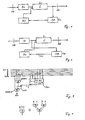
- FIG. 2 shows a block diagram for a circuit arrangement for carrying out the method according to the invention.
- FIG. 3 shows an embodiment for a mode selection computer, and
- FIG. 4 shows a circuit detail in an equivalent form.
- Figure 2 shows essentially the same arrangement as Figure 1, but the difference is that the input of the mode selection computer MR not with the output of the 5B / 6B encoder C but with the output of the buffer B1 for the input signal, which is 5-bit -coded is connected.
- the evaluation of the 5-bit code word of the input signal by the encoder and by the mode selection computer can begin at the same time.
- coding and mode selection are already after a time r 1 ends approximately equal to T 2, so that the next coding and mode selection can be started, while in the arrangement according to FIG. 1, the mode selection can only take place after the coding of 5 bits into a 6 bit word has ended.
- FIG. 3 shows an embodiment for the mode selection computer MR according to the invention. It consists of a first exclusive OR circuit EXOR 1, the four inputs of which are fed by bits B, C, D, E of the 5-bit coded data input signal. The output of this EXOR gate leads to the one input of an AND gate AND, the output of which is connected to the one input of a second exclusive OR gate EXOR 2 and the input of which is fed via an inverting stage from the output of a decoder gate Dec.
- the decoder Dec is acted on the input side by all 5 bits of the data input signal and by a binary signal mode which accepts one of the two binary signals 0 or 1, depending on whether the current mode is a positive or a negative one.
- the decoding circuit Dec generates a binary 1 at its output Y if the input contains 5-bit code word 11 or 20, 5-bit code word 7 in negative or 24 in positive current mode. Since the second input of the second exclusive OR gate EXOR 2 is acted upon by the binary signal for the current mode mode, the binary signal for the subsequent mode appears at the output FM of this gate, whereby in the event of an odd number of ones in the last four bits of the 5th -Bit-coded input signal, i.e. in B, C, D and E the mode for the following code word is inverted.
- the instantaneous mode is also used for the following 5- Keep bit code word. That way achieved a coding according to Table 1 (see claim 1).
- FIG. 4 shows the equivalence of an exclusive OR circuit with four inputs and three exclusive OR circuits with two inputs each, in a tree structure.
- the decoding circuit Dec according to FIG. 3 can be implemented in the usual way by means of logic logic elements according to the known rules of logic logic.
Landscapes
- Physics & Mathematics (AREA)
- Spectroscopy & Molecular Physics (AREA)
- Engineering & Computer Science (AREA)
- Computer Networks & Wireless Communication (AREA)
- Signal Processing (AREA)
- Compression, Expansion, Code Conversion, And Decoders (AREA)
Applications Claiming Priority (2)
| Application Number | Priority Date | Filing Date | Title |
|---|---|---|---|
| DE3406945 | 1984-02-25 | ||
| DE3406945 | 1984-02-25 |
Publications (2)
| Publication Number | Publication Date |
|---|---|
| EP0155455A1 true EP0155455A1 (fr) | 1985-09-25 |
| EP0155455B1 EP0155455B1 (fr) | 1988-06-22 |
Family
ID=6228866
Family Applications (1)
| Application Number | Title | Priority Date | Filing Date |
|---|---|---|---|
| EP85100614A Expired EP0155455B1 (fr) | 1984-02-25 | 1985-01-22 | Dispositif de codage d'un signal numérique |
Country Status (2)
| Country | Link |
|---|---|
| EP (1) | EP0155455B1 (fr) |
| DE (1) | DE3563503D1 (fr) |
Cited By (1)
| Publication number | Priority date | Publication date | Assignee | Title |
|---|---|---|---|---|
| EP0491868A4 (en) * | 1989-09-12 | 1992-10-21 | Tandem Computers Incorporated | Error detection for fiber distributed interfaced optic link |
Citations (3)
| Publication number | Priority date | Publication date | Assignee | Title |
|---|---|---|---|---|
| US3405235A (en) * | 1963-03-12 | 1968-10-08 | Post Office | Systems for transmitting code pulses having low cumulative displarity |
| US3631471A (en) * | 1968-12-13 | 1971-12-28 | Post Office | Low disparity binary codes |
| EP0064097A2 (fr) * | 1981-04-30 | 1982-11-10 | Siemens Aktiengesellschaft | Procédé pour la conversion des signaux d'entrées numériques pour systèmes de transmission par guides d'ondes optiques |
-
1985
- 1985-01-22 EP EP85100614A patent/EP0155455B1/fr not_active Expired
- 1985-01-22 DE DE8585100614T patent/DE3563503D1/de not_active Expired
Patent Citations (3)
| Publication number | Priority date | Publication date | Assignee | Title |
|---|---|---|---|---|
| US3405235A (en) * | 1963-03-12 | 1968-10-08 | Post Office | Systems for transmitting code pulses having low cumulative displarity |
| US3631471A (en) * | 1968-12-13 | 1971-12-28 | Post Office | Low disparity binary codes |
| EP0064097A2 (fr) * | 1981-04-30 | 1982-11-10 | Siemens Aktiengesellschaft | Procédé pour la conversion des signaux d'entrées numériques pour systèmes de transmission par guides d'ondes optiques |
Cited By (1)
| Publication number | Priority date | Publication date | Assignee | Title |
|---|---|---|---|---|
| EP0491868A4 (en) * | 1989-09-12 | 1992-10-21 | Tandem Computers Incorporated | Error detection for fiber distributed interfaced optic link |
Also Published As
| Publication number | Publication date |
|---|---|
| DE3563503D1 (en) | 1988-07-28 |
| EP0155455B1 (fr) | 1988-06-22 |
Similar Documents
| Publication | Publication Date | Title |
|---|---|---|
| DE3784617T2 (de) | Digital-analog-wandler. | |
| DE69321022T2 (de) | Kodierte Modulation mit Verwendung einer Kombination von Faltungs- und Blockkodierung | |
| DE2210649C3 (de) | Nachrichtenübertragungssystem mit Binär-Vielpegel-Kodewandler und Vielpegel-Binär-Kodewandler | |
| DE69106580T2 (de) | Codieranordnung mit einem Unterbandcoder und Sender mit der Codieranordnung. | |
| DE2320422A1 (de) | Verfahren zur fehlererkennung | |
| DE2030827A1 (de) | Vorcodierte ternare Datenubertragungs anlage | |
| DE3015849A1 (de) | Verfahren und vorrichtung zur modulation und demodulation von daten | |
| DE69427339T2 (de) | Begrenzerschaltung | |
| EP1155498B1 (fr) | Dispositif et procede pour produire un flux de donnees, et dispositif et procede pour lire un flux de donnees | |
| DE19605418A1 (de) | Verfahren zur Aufbereitung von Daten, insbesondere für die Übertragung mit veränderlicher Kanalbitrate | |
| DE3500115A1 (de) | Verfahren zum codieren eines datenbitmusters, anordnung zur durchfuehrung des verfahrens und anordnung zum decodieren des mit dem verfahren erhaltenen kanalbitflusses | |
| DE69129622T2 (de) | Hybrid-analog-digital-signalverarbeitung | |
| EP0155455B1 (fr) | Dispositif de codage d'un signal numérique | |
| DE4223639C1 (de) | Verfahren zum Übertragen zweier voneinander unabhängiger digitaler Signale | |
| DE69021274T2 (de) | Anordnung zum Detektieren von Nulldurchgängen. | |
| DE2103312A1 (de) | Verfahren und Schaltungsanordnungen zur Binardatenubertragung über einen Kanal begrenzter Bandbre te | |
| DE69002479T2 (de) | Verfahren und Vorrichtung zur Informationsübertragung zwischen Stationen eines Kommunikationsnetzwerkes, insbesondere für Kraftwagen. | |
| DE3822324A1 (de) | Vorrichtung zum zerlegen des prioritaetswertes | |
| DE2702746C3 (de) | Verfahren und Schaltung zum Codieren von Faksimilesignalgen | |
| DE69815541T2 (de) | Verfahren und vorrichtung zur viterbi-dekodierung von punktierten codes | |
| DE68923736T2 (de) | Dekoder für Hamming kodierte Daten. | |
| DE4137609C2 (de) | Kombiniertes Sprach- und Kanaldecodierverfahren | |
| DE69935487T2 (de) | Verfahren und Vorrichtung zur Blockkodierung | |
| DE3933822A1 (de) | Verfahren zum codieren und decodieren von binaeren daten sowie einrichtung zur durchfuehrung des verfahrens | |
| EP0984355A2 (fr) | Appareil pour la détermination rapide des n valeurs les plus grandes, ou n est un nombre présélectionné |
Legal Events
| Date | Code | Title | Description |
|---|---|---|---|
| PUAI | Public reference made under article 153(3) epc to a published international application that has entered the european phase |
Free format text: ORIGINAL CODE: 0009012 |
|
| AK | Designated contracting states |
Designated state(s): DE FR GB IT |
|
| 17P | Request for examination filed |
Effective date: 19851024 |
|
| 17Q | First examination report despatched |
Effective date: 19861001 |
|
| ITF | It: translation for a ep patent filed | ||
| GRAA | (expected) grant |
Free format text: ORIGINAL CODE: 0009210 |
|
| AK | Designated contracting states |
Kind code of ref document: B1 Designated state(s): DE FR GB IT |
|
| REF | Corresponds to: |
Ref document number: 3563503 Country of ref document: DE Date of ref document: 19880728 |
|
| GBT | Gb: translation of ep patent filed (gb section 77(6)(a)/1977) | ||
| ET | Fr: translation filed | ||
| PLBE | No opposition filed within time limit |
Free format text: ORIGINAL CODE: 0009261 |
|
| STAA | Information on the status of an ep patent application or granted ep patent |
Free format text: STATUS: NO OPPOSITION FILED WITHIN TIME LIMIT |
|
| 26N | No opposition filed | ||
| ITTA | It: last paid annual fee | ||
| REG | Reference to a national code |
Ref country code: GB Ref legal event code: 746 |
|
| REG | Reference to a national code |
Ref country code: FR Ref legal event code: DL |
|
| PGFP | Annual fee paid to national office [announced via postgrant information from national office to epo] |
Ref country code: DE Payment date: 19941222 Year of fee payment: 11 |
|
| PGFP | Annual fee paid to national office [announced via postgrant information from national office to epo] |
Ref country code: GB Payment date: 19960105 Year of fee payment: 12 |
|
| PGFP | Annual fee paid to national office [announced via postgrant information from national office to epo] |
Ref country code: FR Payment date: 19960115 Year of fee payment: 12 |
|
| PG25 | Lapsed in a contracting state [announced via postgrant information from national office to epo] |
Ref country code: DE Effective date: 19961001 |
|
| PG25 | Lapsed in a contracting state [announced via postgrant information from national office to epo] |
Ref country code: GB Effective date: 19970122 |
|
| GBPC | Gb: european patent ceased through non-payment of renewal fee |
Effective date: 19970122 |
|
| PG25 | Lapsed in a contracting state [announced via postgrant information from national office to epo] |
Ref country code: FR Effective date: 19970930 |
|
| REG | Reference to a national code |
Ref country code: FR Ref legal event code: ST |