EP0155499A2 - Dispositif de commande d'affichage - Google Patents
Dispositif de commande d'affichage Download PDFInfo
- Publication number
- EP0155499A2 EP0155499A2 EP85101561A EP85101561A EP0155499A2 EP 0155499 A2 EP0155499 A2 EP 0155499A2 EP 85101561 A EP85101561 A EP 85101561A EP 85101561 A EP85101561 A EP 85101561A EP 0155499 A2 EP0155499 A2 EP 0155499A2
- Authority
- EP
- European Patent Office
- Prior art keywords
- data
- display control
- display
- control unit
- register
- Prior art date
- Legal status (The legal status is an assumption and is not a legal conclusion. Google has not performed a legal analysis and makes no representation as to the accuracy of the status listed.)
- Granted
Links
Images


Classifications
-
- G—PHYSICS
- G09—EDUCATION; CRYPTOGRAPHY; DISPLAY; ADVERTISING; SEALS
- G09G—ARRANGEMENTS OR CIRCUITS FOR CONTROL OF INDICATING DEVICES USING STATIC MEANS TO PRESENT VARIABLE INFORMATION
- G09G5/00—Control arrangements or circuits for visual indicators common to cathode-ray tube indicators and other visual indicators
- G09G5/001—Arbitration of resources in a display system, e.g. control of access to frame buffer by video controller and/or main processor
-
- G—PHYSICS
- G09—EDUCATION; CRYPTOGRAPHY; DISPLAY; ADVERTISING; SEALS
- G09G—ARRANGEMENTS OR CIRCUITS FOR CONTROL OF INDICATING DEVICES USING STATIC MEANS TO PRESENT VARIABLE INFORMATION
- G09G2360/00—Aspects of the architecture of display systems
- G09G2360/12—Frame memory handling
- G09G2360/127—Updating a frame memory using a transfer of data from a source area to a destination area
-
- G—PHYSICS
- G09—EDUCATION; CRYPTOGRAPHY; DISPLAY; ADVERTISING; SEALS
- G09G—ARRANGEMENTS OR CIRCUITS FOR CONTROL OF INDICATING DEVICES USING STATIC MEANS TO PRESENT VARIABLE INFORMATION
- G09G5/00—Control arrangements or circuits for visual indicators common to cathode-ray tube indicators and other visual indicators
- G09G5/22—Control arrangements or circuits for visual indicators common to cathode-ray tube indicators and other visual indicators characterised by the display of characters or indicia using display control signals derived from coded signals representing the characters or indicia, e.g. with a character-code memory
- G09G5/24—Generation of individual character patterns
- G09G5/246—Generation of individual character patterns of ideographic or arabic-like characters
-
- G—PHYSICS
- G09—EDUCATION; CRYPTOGRAPHY; DISPLAY; ADVERTISING; SEALS
- G09G—ARRANGEMENTS OR CIRCUITS FOR CONTROL OF INDICATING DEVICES USING STATIC MEANS TO PRESENT VARIABLE INFORMATION
- G09G5/00—Control arrangements or circuits for visual indicators common to cathode-ray tube indicators and other visual indicators
- G09G5/36—Control arrangements or circuits for visual indicators common to cathode-ray tube indicators and other visual indicators characterised by the display of a graphic pattern, e.g. using an all-points-addressable [APA] memory
- G09G5/39—Control of the bit-mapped memory
- G09G5/393—Arrangements for updating the contents of the bit-mapped memory
-
- G—PHYSICS
- G09—EDUCATION; CRYPTOGRAPHY; DISPLAY; ADVERTISING; SEALS
- G09G—ARRANGEMENTS OR CIRCUITS FOR CONTROL OF INDICATING DEVICES USING STATIC MEANS TO PRESENT VARIABLE INFORMATION
- G09G5/00—Control arrangements or circuits for visual indicators common to cathode-ray tube indicators and other visual indicators
- G09G5/36—Control arrangements or circuits for visual indicators common to cathode-ray tube indicators and other visual indicators characterised by the display of a graphic pattern, e.g. using an all-points-addressable [APA] memory
- G09G5/39—Control of the bit-mapped memory
- G09G5/395—Arrangements specially adapted for transferring the contents of the bit-mapped memory to the screen
Definitions
- the present invention relates to an improved display control unit for computer systems.
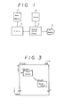
- Fig; 1 there is illustrated a block diagram of a conventional color graphics display unit.
- a CPU microprocessor
- main memory 2 is dedicated to holding programs and data
- display control circuit 3 is used to control the color graphics display.
- Reference character 4 designates a VRAM (video memory) to hold data for CRT display
- character 5 represents a CRT color display unit.
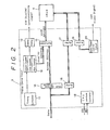
- Fig. 2 shows a block diagram of an example of the display control circuit 3 illustrated in Fig. 1.
- a timing controller 11 generates a ⁇ clock signal which is in turn inputted to a counter 12 having a column counter and a line counter. This counter 12 is then operated to generate a synchronous signal for CRT display via a display timing circuit 13. On the other hand, the counter 12 creates display addresses which are then outputted as VRAM addresses via a multiplexer 15.
- Read data for display access coming from VRAM 4 are inputted to a video output controller 20 via a buffer 1S to produce CRT video signals.
- VRAM address register 14 When CPU 1 tries to access VRAM 4, the addresses of VRAM 4 are set in a VRAM address register 14. And, if a write strobe is input to a CPU interface controller 18, then the multiplexer 15 selects the outputs of the VRAM address register 14 given by CPU 1 as VRAM addresses, and also the write data from CPU 1 is written into VRAM 4 via buffers 16, 17.
- Fig. 3 illustrates an example of the VRAM 4 which has a series of physical addresses as a memory unit. Logically, it has a display screen as shown and the display screen ccmprises 256 horizontal dots x 1024 vertical dots.
- a display screen is physically composed of 200 vertical dots. Therefore, the logical existence of 1024 vertical dots means that the screen has unobserved areas or that a plurality of screens are present.
- CPU 1 calculates the physical addresses of the VRAM 4 based on the coordinates (Sx, Sy) in the source area and then sets them in the VRAM address register 14 within the display control circuit 3.
- CPU 1 also produces a read command output so as to read the color code data within the VRAM 4 corresponding to the coordinates (Sx, Sy).
- CPU 1 calculates the physical addresses within the VRAM 4 based on the coordinates (Dx, Dy) in the destination area to which the data is to be transferred and sets them in the VRAM address-register 14 within the display control circuit 3.
- CPU 1 outputs a read command to read the color code data within the VRAM 4 corresponding to the coordinates (Dx, Dy), and then obtains the OR of (i.e., ORs) the color code data within the VRAM 4 and the color code data from the above-mentioned coordinates (Sx, Sy).
- CPU 1 outputs a write command to write the ORed color code data into the VRAM 4, in particular, a location of the VRAM 4 corresponding to the coordinates (Dx, Dy).
- the above-mentioned Read/Read/Logical operation/Write sequence is repeated NX times with respect to a horizontal direction and NY times with respect to a vertical direction (that is, NX X NY times) so as to superpose the source area color code data on the destination area color code data.
- CPU 1 and Display Control Circuit 3 are operated independently of each other, and the display timing of the display control circuit 3 has priority over the VRAM timing of the CPU 1. As a result of this, a wait time arises in access from CPU 1 to VRAM 4, which results in the extremely deteriorated efficiency of the data transfer.
- the software must share a heavy load in the display control and thus it takes a very long time to execute its operation.
- a computer is upgraded with increased display specifications and with a plurality of display modes, then its address calculation becomes more complicated and thus it will take an extendes period of time to perform its running operation.
- the following are necessary to replace the CPU processing mode during a retrace period by that during a display period; to speed up the updating process of specifying color in the color data; to perform a logical operation for only desired dots on the display screen; and, to transfer at higher speeds a form or an object having a solid body on a transparent background within a source area. Further, it is desired to be able to display "kanji" pattens fast so as to facilitate accomodation of the kanji.
- the present invention aims at eliminating the drawbacks in the above-mentioned prior art display control unit as well as meeting the demands currently requested in the market.
- an improved display control unit in which the processing form of its CPU can be modified, that is, when the execution time of its display operation is reduced by reading out data in a source area from within a memory unit and sequentially writing the read-out data into a destination area, a predetermined period of time before the begining of a vertical retrace the CPU is interrupted so that the CPU can omit its confirmation as to whether a video CPU has completed its previous processing
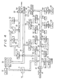
- FIG. 4 there is illustrated a block diagram of an embodiment of the invention.
- a clock generator 31 to generate a display timing clock and a counter 32 which comprises a column counter to generate a CRT screen display timing and a VRAM address in accordance with the display timing clock, a line counter, and a row counter.
- Data bus 41 from CPU 1 is connected via Buffer 42 to Register bus 43.
- the number of registers within a display control circuit 3 accessed by CPU 1 is held by a register pointer/counter 44 and the outputs of this register pointer/ counter 44 are decoded by a register selector decoder 45, so that the registers can be specified individually.
- the register pointer/counter 44 has a count-up function. That is, in setting parameters of the respective registers, after one setting has been completed, it counts up 1. Thus, the registers can be automatically specified successively one by one.
- Command Register 46 holds the command information from CPU 1, and Video CPU 47 processes the display data in accordance with the commands from CPU 1.
- SR Register 48 holds the status from Video CPU 47 to CPU 1.
- CPU 1 specifies the physical address of VRAM 4 to access the VRAM 4, the VRAM address is to be held by VRAM Address Register/Counter 37.
- Color Code Register 33 holds the read data from VRAM 4 as well as the write data to VRAM 4.
- DX Register/Counter 58 to hold the values on the horizontal X coordinates of a destination area
- DY Register/Counter 59 to hold the values on the vertical Y coordinates of the same
- DX Address Composing circuit 57 to create the physical address of VRAM 4 in accordance with the respective outputs of DX, DY Register/Counters 58, 59.
- VRAM Address Bus 36 which is contained within the display control circuit 3, is connected through Buffer 55 to Address Line 56 of VRAM 4.
- VRAM Data Bus 35 which is also contained in the display control circuit 3, is connected through Buffer 53 to VRAM Data Line 54.
- NX Register 61 holds the transfer data number in a horizontal direction (that is, a direction of the X coordinates), while NY Register 63 holds the transfer data number in a vertical direction (that is, a direction of the Y coordinates).
- a horizontal direction flag 60 which points to a positive direction (or, right direction) when it is "0" and points to a negative direction (or, left direction) for "0".
- a vertical direction flag 62 indicates a positive direction (or, downward direction) when it is "0", and a negative direction (or, upward direction) for "1".
- S Register 34 holds the read data from the source area
- D Register 52 holds the read data from the destination area.
- ALU (arithmetic and logic unit) 51 performs logical operations such as IMP, AND, OR, EOR, NOT operations of the outputs of S Register 34, Color Code Register 33 and D Register 52 in accordance with the control from Video CPU 47.
- Interrupt line (IL) Register 70 is used to previously set the number of columns, lines, or rows for IL interruptions, while Comparator 71 is dedicated to detecting the correspondence of the number of the columns, lines, or rows set by IL Register 70.
- Source Data Bit Selector 101 selects higher 4 bits or lower 4 bits from the source data and then uses the selected 4 bits to form higher 4 bits or lower 4 bits.
- Byte Data Selector 102 selects the data which has passed through Source Data Bit Selector 101 or the source data from S Register 34.
- Transparence Detection Circuit 104 serves to detect a color code (that is, transparency) for a portion of the source area in which no object exists.
- Parallel Bit Selector 103 causes omission of logical operations of some of the color codes within the destination area which corresponds to the color code within the source area, provided that the very source area color code happens to be transparent.
- Expansion Memory 111 is used as "kanji” ROM(Pattern Memory) or a buffer area.
- Slot Switch 121 is dedicated to switching a video request or a process request.
- ARGR Switch 123 is used to switch a request to a video request or a process request in accordance with the respective bits of an argument register.
- the foregoing elements are the characteristic ones of the present invention. Although there exist other elements than the foregoings in the display control circuit 3, an explanation is omitted here regarding such elements as not necessary in describing the operation of the invention.
- the operation of the display control circuit 3 is described, by way of example, in connection with the block data transfer/superposition based on X, Y coordinates.
- CPU 1 has previously set information necessary for the logical operation and block data transfer in the respective registers of the display control circuit 3.
- CPU 1 sets the register number of a register to be accessed in a register pointer/counter 44 and thereafter performs its read/write operation.
- SX Register/Counter 38 is composed of SXL (Register #32) and SXH (Register #33)
- SY Register/ Counter 39 is composed of SYL (Register #34) and SYH (Register #35). Therefore, CPU 1 sets a 4-byte parameter on the transfer starting point or the starting coordinates (SX, SY).
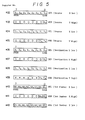
- FIG. 5 illustrates the contents of Registers #32 - 42
- Fig. 6 illustrates the contents of Registers #43 - 46 as well as the contents of Registers #2, #8.
- DX Register/Counter 58 is composed of DXL(Register #36) and DXH(Register #37), while DY Register/Counter 59 is composed of y YL(Register #38) and DYH(Register #39).
- NX Register 61 is composed of NXL (Register #40) and NXH (Register #41)
- NY Register 63 is composed of NYL (Register #42) and NYH (Register #43).
- Direction Flag 60 corresponds to the bit 3 of Argument Register ARGR (Register #45), and Direction Flag 62 to the bit 2 of Argument Register ARGR (Register #45).
- Fig. 7 is a table to illustrate command codes.
- VDC stands for the display control circuit 3.
- Fig. 8 is a table to illustrate logical operations.
- SC represents a source color code and DC stands for a destination color code.
- CPU 1 creates command codes such as "10010010" in accordance with the above-mentioned command codes and logical operation codes and then sets them in Command Register 45 (Register #45).
- the higher 4 bits of the above-mentioned command code express an instruction to transfer a block data within VRAM 4 provided that the source area and the destination area are both present within the VRAM 4.
- the lower 4 bits of the above example represent a logical operation code, that is, "0010" means that the OR of the source color code data and the destination color code data before transferred is to be written into the destination.
- Video CPU 47 sets the command executing (CE) of the bit 7 of SR Register 48 to initiate the execution and processing of the command.
- SXY Address Composing Circuit 40 is operated to create a physical address of VRAM 4 from SX Register/Counter 38 and SY Register/Counter 39 respectively holding the source area coordinates under control of Video CPU 47. According to this physical address, a color code data is read out from VRAM 4, which read-out data is in turn set in S Register 34 through Data Line 54, Buffer 53, and VRAM Data Bus 35.
- DXY Address Composing Circuit 57 is operated to create a physical address of VRAM 4 from the outputs of DX Register/Counter 58 and DY Register/Counter 59 respectively holding the destination area coordinates. According to this physical address, a color code data is read from VRAM 4, which data is in turn set in D Register 52.
- a color code data within S Register 34 read out from the source side and a color code data in D Register 52 read out from the destination side are ORed by ALU (Arithmetic and Logic Unit) 51 to produce a superposed color code data.
- ALU Arimetic and Logic Unit
- the newly operated and produced color code data is output on VRAM Data Line 54 via VRAM Data Bus 35 and Buffer 53, and is then written into VRAM 4 in accordance with a physical address on the destination side produced by DXY Address Composing Circuit 57.
- Video CPU 47 decides that the logical operation (OR)/ block data transfer has been completed, clears the command executing (CE) bit within SR Register 48, and informs CPU 1 of the end of the command.
- CPU 1 After confirming that this TR bit is "1", CPU 1 sets a next transfer data in Color Code Register 33. This resets the TR bit and returns it to its original status. Other operations are the same as with the above-mentioned block data transfer within VRAM 4.
- a color code data from CPU 1 (that is, a fixed data) is set into D Register 52 via Color Code Register 33.
- the color code data after operated, is set in Color Code Register 33 and is then read by CPU 1.
- Video CPU 47 reads out a transfer data from VRAM 4 in accordance with SX Register/counter 38 and SY Register/counter 39 and sets the read-out transfer data in Color Code Register 33, and at the same time sets the TR bit of SR Register 48 for ''1".
- CPU 1 checks this TR bit, and, if it is "1", then CPU 1 reads out the transfer data from Color Code Register 33. As a result of this, the TR bit is reset and returns to its initial status. Other operations are performed in the same way as in the above-mentioned data transfer within VRAM 4.
- the data written into Color Code Register 33 is transferred to the destination area of VRAM 4. This is an effective way in writing the same data.
- the procedure of this operation is the same as in the above-mentioned block data transfer from CPU 1 to VRAM 4. However, in this instance, CPU 1 is required to write the data into Color Code Register 33 only once, and the data is to be transferred under control of Video CPU 47.
- a vertical return line period is longer than a horizontal retrace period and thus it takes longer time to process commands in the vertical retrace period than in the horizontal retrace line period. Accordingly, if it is possible to employ such a command processing system as can avoid the waiting of CPU 1 in the vertical period, then the performance of the display control unit can be enhanced substantially. To this end, when the vertical retrace period comes near, an interrupt (or, IL interrupt) is caused to occur to inform CPU 1 of the effect.
- an interrupt or, IL interrupt
- Such IL interrupt is enabled by previously having set the value of Vertical Counter (Line, Row) 32 in IL Register 70 shown in Fig. 4 (an interrupt line register, #8 Register shown in Fig. 6).
- the value to be set for this purpose may be the start line number of the vertical retrace or, in case when the overhead time for interrupt processing is long, such a value may be set as causes an interrupt to take place earlier by such long time. In either event, it is possible to improve the efficency of the display control unit.
- SR Register 48 shown in Fig. 4 (a status register, or #2 Register shown in Fig. 6) is sometimes checked for its VR bit (that is, the output of the VR status signal produced by decoding the out- put of Counter 32 is read out) to decide whether a processing in the very vertical retrace is to be continued or not.
- the above-mentioned VR bit is produced by decoding the out-put of Counter 32 such that it becomes "0" a predetermined time before the termination of the vertical retrace line period. It is necessary to set up the predetermined time duration even when a processing happens to be longest during the vertical retrace so as to prevent such longest processing from being carried over into the display period.
- the status of the horizontal retrace can also be shifted forwardly in time to increase its processing efficency.
- the leading edge of the timing may be shifted before a minimum time duration required to issue a VRAM access after detection of the HR bit, and the trailing edge thereof may be staggered before more than the maximum time duration.
- Fig. 9 illustrates the timing mentioned above.
- the predetermined time duration from the beginning of the vertical or horizontal retrace necessary to cause an interrupt to CPU 1 may be changed depending upon the time periods from the generation of an interrupt signal to CPU 1 to the initiation of the interrupt processing. Also, this predetermined time duration must be changed in accordance with the length of the execution time of programs.
- the processing mode of CPU 1 is changed by causing CPU 1 to omit the confirmation as to whether Video CPU 47 has completed its previous processing, and at the same time a status signal to indicate the then processing is present within the retrace period is monitored so as to continue to change the processing mode of CPU 1.
- the status signal has been previously extinguished within a predetermined time after the termination of the retrace. Then, the processing mode of CPU-1 is returned to its original way, in which CPU 1 confirms whether Video CPU 47 has completed its previous processing.
- Fig. 10 illustrates a block diagram of another embodiment of the invention, showing an example in which an updating processing.of color specification in the display data can be performed at increased speeds.
- a memory interface consists of a byte(8 bits) or a word (16 - 32 bits) and thus contains information on display of a plurality of dots. In this case, when the dots are to be processed one by one, the remaining bits must be masked.
- Source Data Selector 101 selects higher 4 bits when 0 bit of SXY is "0", and lower 4 bits when this 0 bit is "I”. The data is then transferred via Byte Data Selector 102 to ALU 51. In ALU 51, a logical operation of the data and the value of D Register 52 is executed for each bit. After then, Parallel Bit Selector 103 outputs as VRAM data either 4 bits (that is, the upper 4 bits for "O", the lower 4 bits for "1") to be specified in accordance with the value of the bit 0 of DXY.
- Transparency Detection Circuit 104 decides the source data as transparent and thus Parallel Bit Selector 103 allows the value of D Register 52 as it is to pass through.
- bit select/mask function and transparency processing can be realized.
- the color code data within the source area and the color code data within the destination area are logically operated, while a portion belonging to the source area and having no object existing therein, more particularly the color code (transparent color) of such portion is detected -by Transparency Detection Circuit 104 and the logical operation of the transparent portion is omitted, so that only the form stored in the source area and having a solid body can be transferred at high speeds.
- Source data specified by a: source address is divided into a plurality of portions and one of the data portions is then selected, while destination data specified by a destination address is also divided into a plurality of data portions and one of the data portions is selected. After logical operations are performed on the thus selected data portions, the logical operation result or the destination data is selected for each of the portions of the respective data. As a result of this, it is possible to perform logical operations only on a desired dot on the display screen.
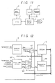
- Fig. 11 is a block diagram of another embodiment of the invention, illustrating an example using an expansion memory as a "kanji"(chinese-character) accomodation or as a buffer area.
- Expansion Memory 111 is extended in parallel with VRAM 4.
- this expansion memory 111 is extended in parallel with VRAM 4 as a chinese-character pattern ROM
- chinese characters (“kanji") can be accommodated.
- a high-speed display can be realized by transferring a chinese-character pattern to VRAM 4 by means of area movement.
- the read speed of the chinese-character pattern ROM, or the cycle time of the area movement in this case may be slower than the display memory access, low-speed and large- capacity memory elements can be used.
- an address register may be located within the expansion memory and, at the time when the previous access has been completed, an address may be updated to initiate the next reading.
- MXC which serves to switch and control the VRAM access from CPU 1 makes it possible to directly read and write an expansion memory from CPU 1.
- MXD specifies the destination area to the expansion memory and makes it possible for the expansion memory to be read and written as the data memory.
- MXS specifies the source area to the expansion memory and permits reading of a fixed pattern or reading from a buffer memory.
- Fig. 12 is a circuit diagram of the main portions of the embodiment shown in Fig. 11.
- Access requests for a memory are normally classified into two main categories; namely, video requests (VRQ) and process requests (PRQ).
- the video requests VRQ are requests for reading of data for CRT display and are issued based on the counts of Counter 32.
- the process requests PRQ are VRAM accesses that are issued by Video CPU. This issue results from the controls of CPU such as setting of parameters from CPU 1, starting of commands, VRAM access and the like.
- the video requests VRQ and process requests PRQ are controlled by timing control signals, and are respectively permitted by the allocated time slots. These operations are processed by Slot Switch 121 shown in Fig. 12. That is, at a timing when the video request VRQ is issued,Slot Switch 121 is always connected to the video request VRQ side, and in other cases it is connected to the process request PRQ side. Thus, PRQ is permitted only when Slot Switch 121 is connected to the PRQ side.
- the contents of the process request PRQ are classified into CRQ to be issued when CPU 1 accesses VRAM 4 directly, DRQ issued when the destination data is accessed while Video CPU 122 is executing a command, and SRQ issued when the source data is accessed.
- These requests are normally connected to the process request PRQ side by ARGR Switch 123.
- This ARGR Switch 123 is adapted to connect the requests, CRQ, DRQ and SRQ to an XRQ side in accordance with each of the bits MXC, MXD and MXS.
- This XRQ is a memory request (MX request) to the expansion memory, and when the XRQ appears the expansion memory is to be accessed instead of VRAM 4.
- the expansion memory can be used as a buffer memory or a pattern memory.
- MXD and VRAM 4 by MXS to specify the area movement
- VRAM 4 and the expansion memory are specified by MXD and MXS respectively, then it is possible to return the saved data to its original state, or to move a fixed pattern (or, a chinese-character pattern) to VRAM 4 for display.
- the present invention is useful in performing display control of not only the color CRT but also other display units such as a monochrome CRT, LCD, plasma, and EL.
- the present invention provides several effects: namely, when reducing the execution time for display operation by reading out the source area data from a memory unit and then writing the read-out source area data sequentially into the destination area, the command processing speed can be increased during a vertical or horizontal retrace line period; it is possible to increase the speed of an update processing on color specification in display data, and at the same time only a desired dot on the display screen can be logically operated; and, it is possible to transfer a form or an object existing within the source area and having a solid body at high speeds, and an expansion memory can be used as a "kanji" (chinese-character) ROM (or, a pattern memory) or a buffer area.
- kanji chinese-character
Landscapes
- Engineering & Computer Science (AREA)
- Multimedia (AREA)
- Physics & Mathematics (AREA)
- Computer Hardware Design (AREA)
- General Physics & Mathematics (AREA)
- Theoretical Computer Science (AREA)
- Controls And Circuits For Display Device (AREA)
Applications Claiming Priority (2)
| Application Number | Priority Date | Filing Date | Title |
|---|---|---|---|
| JP28784/84 | 1984-02-20 | ||
| JP59028784A JPS60173580A (ja) | 1984-02-20 | 1984-02-20 | 表示制御装置 |
Publications (3)
| Publication Number | Publication Date |
|---|---|
| EP0155499A2 true EP0155499A2 (fr) | 1985-09-25 |
| EP0155499A3 EP0155499A3 (en) | 1990-09-12 |
| EP0155499B1 EP0155499B1 (fr) | 1993-01-07 |
Family
ID=12258041
Family Applications (1)
| Application Number | Title | Priority Date | Filing Date |
|---|---|---|---|
| EP85101561A Expired - Lifetime EP0155499B1 (fr) | 1984-02-20 | 1985-02-13 | Dispositif de commande d'affichage |
Country Status (4)
| Country | Link |
|---|---|
| EP (1) | EP0155499B1 (fr) |
| JP (1) | JPS60173580A (fr) |
| CA (1) | CA1228931A (fr) |
| DE (1) | DE3586954T2 (fr) |
Cited By (5)
| Publication number | Priority date | Publication date | Assignee | Title |
|---|---|---|---|---|
| GB2210239A (en) * | 1987-09-19 | 1989-06-01 | Hudson Soft Co Ltd | An apparatus for controlling the access of a video memory |
| GB2246935A (en) * | 1987-09-19 | 1992-02-12 | Hudson Soft Co Ltd | An apparatus for the control of an access to a video memory |
| US7800621B2 (en) | 2005-05-16 | 2010-09-21 | Ati Technologies Inc. | Apparatus and methods for control of a memory controller |
| US7827424B2 (en) * | 2004-07-29 | 2010-11-02 | Ati Technologies Ulc | Dynamic clock control circuit and method |
| US8799685B2 (en) | 2010-08-25 | 2014-08-05 | Advanced Micro Devices, Inc. | Circuits and methods for providing adjustable power consumption |
Family Cites Families (9)
| Publication number | Priority date | Publication date | Assignee | Title |
|---|---|---|---|---|
| US4197590A (en) * | 1976-01-19 | 1980-04-08 | Nugraphics, Inc. | Method for dynamically viewing image elements stored in a random access memory array |
| JPS5326539A (en) * | 1976-08-25 | 1978-03-11 | Hitachi Ltd | Data exchenge system |
| GB2016757A (en) * | 1978-02-21 | 1979-09-26 | Data General Corp | Display Terminal |
| JPS54139431A (en) * | 1978-04-21 | 1979-10-29 | Hitachi Ltd | Crt display unit |
| JPS54139433A (en) * | 1978-04-21 | 1979-10-29 | Hitachi Ltd | Decision system for end of writing |
| US4240140A (en) * | 1978-12-26 | 1980-12-16 | Honeywell Information Systems Inc. | CRT display terminal priority interrupt apparatus for generating vectored addresses |
| JPS5674738A (en) * | 1979-11-21 | 1981-06-20 | Toshiba Corp | Transfer system of display data |
| US4394645A (en) * | 1981-09-10 | 1983-07-19 | Sensormatic Electronics Corporation | Electrical surveillance apparatus with moveable antenna elements |
| JPS5960480A (ja) * | 1982-09-29 | 1984-04-06 | フアナツク株式会社 | デイスプレイ装置 |
-
1984
- 1984-02-20 JP JP59028784A patent/JPS60173580A/ja active Pending
-
1985
- 1985-02-13 DE DE19853586954 patent/DE3586954T2/de not_active Expired - Fee Related
- 1985-02-13 EP EP85101561A patent/EP0155499B1/fr not_active Expired - Lifetime
- 1985-02-19 CA CA000474619A patent/CA1228931A/fr not_active Expired
Cited By (7)
| Publication number | Priority date | Publication date | Assignee | Title |
|---|---|---|---|---|
| GB2210239A (en) * | 1987-09-19 | 1989-06-01 | Hudson Soft Co Ltd | An apparatus for controlling the access of a video memory |
| GB2246935A (en) * | 1987-09-19 | 1992-02-12 | Hudson Soft Co Ltd | An apparatus for the control of an access to a video memory |
| GB2246935B (en) * | 1987-09-19 | 1992-05-20 | Hudson Soft Co Ltd | An apparatus for the control of an access to a video memory |
| GB2210239B (en) * | 1987-09-19 | 1992-06-17 | Hudson Soft Co Ltd | An apparatus for controlling the access of a video memory |
| US7827424B2 (en) * | 2004-07-29 | 2010-11-02 | Ati Technologies Ulc | Dynamic clock control circuit and method |
| US7800621B2 (en) | 2005-05-16 | 2010-09-21 | Ati Technologies Inc. | Apparatus and methods for control of a memory controller |
| US8799685B2 (en) | 2010-08-25 | 2014-08-05 | Advanced Micro Devices, Inc. | Circuits and methods for providing adjustable power consumption |
Also Published As
| Publication number | Publication date |
|---|---|
| JPS60173580A (ja) | 1985-09-06 |
| EP0155499A3 (en) | 1990-09-12 |
| CA1228931A (fr) | 1987-11-03 |
| DE3586954T2 (de) | 1993-06-03 |
| EP0155499B1 (fr) | 1993-01-07 |
| DE3586954D1 (de) | 1993-02-18 |
Similar Documents
| Publication | Publication Date | Title |
|---|---|---|
| US5315698A (en) | Method and apparatus for varying command length in a computer graphics system | |
| US5315696A (en) | Graphics command processing method in a computer graphics system | |
| US5717440A (en) | Graphic processing having apparatus for outputting FIFO vacant information | |
| US5046023A (en) | Graphic processing system having bus connection control capable of high-speed parallel drawing processing in a frame buffer and a system memory | |
| EP0318517B1 (fr) | Circuits generateurs d'affichage pour systeme d'ordinateur personnel | |
| US5594473A (en) | Personal computer apparatus for holding and modifying video output signals | |
| US4566005A (en) | Data management for plasma display | |
| US5185597A (en) | Sprite cursor with edge extension and clipping | |
| EP0149188B1 (fr) | Dispositif de commande d'affichage | |
| US5113491A (en) | Pattern drawing system having a processor for drawing the profile of the pattern and a processor for painting the drawn profile | |
| CA1065513A (fr) | Systeme d'affichage electronique | |
| US5321805A (en) | Raster graphics engine for producing graphics on a display | |
| US4893114A (en) | Image data processing system | |
| EP0658858B1 (fr) | Ordinateur graphique | |
| EP0155499B1 (fr) | Dispositif de commande d'affichage | |
| US6344856B1 (en) | Text optimization | |
| US5812150A (en) | Device synchronization on a graphics accelerator | |
| EP0228745A2 (fr) | Dispositif de contrôle d'affichage vidéo à balayage à trame comportant une antémémoire de mise à jour, antémémoire de mise à jour pour application dans un tel dispositif de contrôle, et terminal d'affichage comportant un tel dispositif de contrôle | |
| KR960003072B1 (ko) | 폰트 데이타 처리장치 | |
| EP0223557A2 (fr) | Commande d'affichage dans un système de traitement de données | |
| JPS60176088A (ja) | メモリ拡張方式 | |
| JP2821121B2 (ja) | 表示制御装置 | |
| WO1993004457A2 (fr) | Procede d'adressage pour systeme d'infographie | |
| JP2941688B2 (ja) | グラフィック処理装置 | |
| JP2535841B2 (ja) | 表示制御装置 |
Legal Events
| Date | Code | Title | Description |
|---|---|---|---|
| PUAI | Public reference made under article 153(3) epc to a published international application that has entered the european phase |
Free format text: ORIGINAL CODE: 0009012 |
|
| 17P | Request for examination filed |
Effective date: 19850213 |
|
| AK | Designated contracting states |
Designated state(s): DE FR GB NL |
|
| PUAL | Search report despatched |
Free format text: ORIGINAL CODE: 0009013 |
|
| AK | Designated contracting states |
Kind code of ref document: A3 Designated state(s): DE FR GB NL |
|
| 17Q | First examination report despatched |
Effective date: 19910201 |
|
| GRAA | (expected) grant |
Free format text: ORIGINAL CODE: 0009210 |
|
| AK | Designated contracting states |
Kind code of ref document: B1 Designated state(s): DE FR GB NL |
|
| REF | Corresponds to: |
Ref document number: 3586954 Country of ref document: DE Date of ref document: 19930218 |
|
| ET | Fr: translation filed | ||
| PLBE | No opposition filed within time limit |
Free format text: ORIGINAL CODE: 0009261 |
|
| STAA | Information on the status of an ep patent application or granted ep patent |
Free format text: STATUS: NO OPPOSITION FILED WITHIN TIME LIMIT |
|
| 26N | No opposition filed | ||
| REG | Reference to a national code |
Ref country code: GB Ref legal event code: IF02 |
|
| PGFP | Annual fee paid to national office [announced via postgrant information from national office to epo] |
Ref country code: GB Payment date: 20020125 Year of fee payment: 18 |
|
| PGFP | Annual fee paid to national office [announced via postgrant information from national office to epo] |
Ref country code: FR Payment date: 20020214 Year of fee payment: 18 |
|
| PGFP | Annual fee paid to national office [announced via postgrant information from national office to epo] |
Ref country code: DE Payment date: 20020227 Year of fee payment: 18 |
|
| PGFP | Annual fee paid to national office [announced via postgrant information from national office to epo] |
Ref country code: NL Payment date: 20020228 Year of fee payment: 18 |
|
| PG25 | Lapsed in a contracting state [announced via postgrant information from national office to epo] |
Ref country code: GB Free format text: LAPSE BECAUSE OF NON-PAYMENT OF DUE FEES Effective date: 20030213 |
|
| PG25 | Lapsed in a contracting state [announced via postgrant information from national office to epo] |
Ref country code: NL Free format text: LAPSE BECAUSE OF NON-PAYMENT OF DUE FEES Effective date: 20030901 |
|
| PG25 | Lapsed in a contracting state [announced via postgrant information from national office to epo] |
Ref country code: DE Free format text: LAPSE BECAUSE OF NON-PAYMENT OF DUE FEES Effective date: 20030902 |
|
| GBPC | Gb: european patent ceased through non-payment of renewal fee | ||
| PG25 | Lapsed in a contracting state [announced via postgrant information from national office to epo] |
Ref country code: FR Free format text: LAPSE BECAUSE OF NON-PAYMENT OF DUE FEES Effective date: 20031031 |
|
| NLV4 | Nl: lapsed or anulled due to non-payment of the annual fee |
Effective date: 20030901 |
|
| REG | Reference to a national code |
Ref country code: FR Ref legal event code: ST |