EP0155720A1 - Kaskadenstromquellenanordnung - Google Patents
Kaskadenstromquellenanordnung Download PDFInfo
- Publication number
- EP0155720A1 EP0155720A1 EP85200255A EP85200255A EP0155720A1 EP 0155720 A1 EP0155720 A1 EP 0155720A1 EP 85200255 A EP85200255 A EP 85200255A EP 85200255 A EP85200255 A EP 85200255A EP 0155720 A1 EP0155720 A1 EP 0155720A1
- Authority
- EP
- European Patent Office
- Prior art keywords
- transistor
- emitter
- base
- voltage
- collector
- Prior art date
- Legal status (The legal status is an assumption and is not a legal conclusion. Google has not performed a legal analysis and makes no representation as to the accuracy of the status listed.)
- Granted
Links
- 229920006395 saturated elastomer Polymers 0.000 description 2
- 230000003503 early effect Effects 0.000 description 1
- 238000012886 linear function Methods 0.000 description 1
Images
Classifications
-
- H—ELECTRICITY
- H03—ELECTRONIC CIRCUITRY
- H03F—AMPLIFIERS
- H03F1/00—Details of amplifiers with only discharge tubes, only semiconductor devices or only unspecified devices as amplifying elements
- H03F1/08—Modifications of amplifiers to reduce detrimental influences of internal impedances of amplifying elements
- H03F1/22—Modifications of amplifiers to reduce detrimental influences of internal impedances of amplifying elements by use of cascode coupling, i.e. earthed cathode or emitter stage followed by earthed grid or base stage respectively
-
- G—PHYSICS
- G05—CONTROLLING; REGULATING
- G05F—SYSTEMS FOR REGULATING ELECTRIC OR MAGNETIC VARIABLES
- G05F3/00—Non-retroactive systems for regulating electric variables by using an uncontrolled element, or an uncontrolled combination of elements, such element or such combination having self-regulating properties
- G05F3/02—Regulating voltage or current
- G05F3/08—Regulating voltage or current wherein the variable is DC
- G05F3/10—Regulating voltage or current wherein the variable is DC using uncontrolled devices with non-linear characteristics
- G05F3/16—Regulating voltage or current wherein the variable is DC using uncontrolled devices with non-linear characteristics being semiconductor devices
- G05F3/20—Regulating voltage or current wherein the variable is DC using uncontrolled devices with non-linear characteristics being semiconductor devices using diode- transistor combinations
- G05F3/26—Current mirrors
- G05F3/265—Current mirrors using bipolar transistors only
Definitions
- the invention relates to a cascode current-source arrangement comprising a first and a second transistor whose collector-emitter paths are arranged in series between a first terminal and a common second terminal, and a third transistor connected as a diode, whose base is connected to the base of the second transistor and whose emitter is connected to the common second terminal.
- Such cascode current-source arrangements are generally applicable in integrated circuits and are in particular suitable for use in amplifier circuits as described in Patent Application (PHN 10.955) filed simultaneously with the present Application.
- Such a current-souree arrangement is known from Fig. 2 of United States Patent Specification 4,345,217.
- the collector current of the second transistor is defined by connecting a diode-connected transistor in parallel with the base-emitter junction of this second transistor.
- the collector current of the second transistor then also flows through the collector-emitter path of the first transistor, whose base is at a reference voltage.
- this reference voltage the collector-emitter voltage of the second transistor is then also constant.
- this reference voltage is generally generated by arranging a second diode-connected transistor in series with the first diode-connected transistor, the base of said second diode-connected transistor being connected to the base of the first transistor.
- the collector-emitter voltage of the second transistor is then equal to one base-emitter voltage.
- a disadvantage of this arrangement is that, if the col- )lector of the second transistor is used as a signal input, the lowest voltage attainable on the collector of the first transistor is equal to the sum of the base-emitter voltage, which appears across the collector-emitter path of the second transistor, and the saturation voltage of the first transistor.
- the collector voltage of the second transistor must be as low as possible. This is of particular importance if the current-source arrangement is used with low supply voltages.
- Another disadvantage of this arrangement is that owing to the difference in the collector-emitter voltages of the diode-connected trans ⁇ tor and the second transistor the current flowing through the second transistor is not exactly equal to the current through the diode. Therefore, it is the object of the invention to provide a cascode current-source arrangement which does not have the said disadvantages.
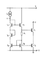
- a cascode current- source arrangement of a type as specified in the opening paragraph is characterized in that it further comprises a first input current path which comprises, between a third terminal and the common second terminal, the series arrangement of a fourth transistor connected as a diode, a diode and the collector-emitter path of a fifth transistor, and a second current path which comprises, between a fourth terminal, connected to the base of the fourth transistor, and the common second terminal, the series arrangement of the base-emitter path of a sixth transistor, a resistor and the base-emitter path of the third transistor, whose base is further connected to the base of the fifth transistor, and the base of the first transistor is connected to that end of the resistor which is remote from the third transistor.
- the collector-emitter voltage of the second transistor is substantially equal to the voltage across the resistor in the second current path.
- the voltage across this resistor can be made substantially lower than one base-emitter voltage, so that the collector of the first transistor can be driven to a very low voltage.
- ithe voltage across this resistor is equal to the collector-emitter voltage of the fifth transistor, so that the collector-emitter voltage of the second transistor is equal to the collector-emitter voltage of the fifth transistor in the input current path, which transistors have also equal base-emitter voltages. Therefore, the ratio between the currents through the second and the fifth transistor is defined accurately by the ratio between the emitter areas of these transistors.
- the arrangement comprises a transistor T and a transistor T 2 connected in cascode, the collector-emitter paths of these transistors being connected in series between an output terminal 2 and the negative power-supply terminal 3, in the present case earth.
- a load may be connected to terminal 2.
- the arrangement further comprises a current-mirror circuit which comprises an input current path which comprises, between an input terminal 4 and the power-supply terminal 3, the series arrangement of a diode-connected transistor T 4 , a diode-connected transistor T 5 , and the collector-emitter path of a transistor T 6 .
- a current source I 1 I is connected to input terminal 4 and to the positive power-supply terminal 5.
- the emitter areas of the transistors T 4 , T 5 and T 6 are, for example, twice as large as the emitter area of the transistor T 7 and transistor T 8 , a current which is substantially equal to 1/2 will flow in the second current path as a result of the commoned bases of the transistors T 4 and T 7 and the commoned bases of the transistors T 6 and T 8 . Since transistors T 4 and T 7 have the same base voltage the voltages between said commoned bases and the negative power-supply terminal 3 in the input current path and the second current path are equal.
- V BE are the base-emitter voltages of the relevant transistors
- V CET6 is the collector-emitter voltage of transistor T 6
- V R is the voltage across the resistor R 1 .
- the base-emitter voltages of the transistors T 4 , T 5 , T 7 and T 8 are equal, so that it follows from equation (1) that If the emitter areas of the transistors T 1 and T 2 are, for example, twice as large as those of the transistors T 49 T 5 and T 6 , the current flowing through transistors T 1 and T 2 will be twice as large as the current in the input current path.
- the voltage between the base of transistor T 4 and the negative power-supply terminal 3 satisfies the following equation: Owing to the ratios between the currents and between the emitter areas of the transistors T 4 , T 5 , T 7 and T 1 it follows from equation (2) that Since the collector-emitter voltages are equal the ratio between the currents in the transistors T 2 and T 6 depends only on the ratio between the emitter areas, so that in the present example the current in transistor T 2 is exactly twice as large as the current in transistor T 6 . Moreover, the voltage on the base of transistor T is constant because a constant current of about I/2 flows through the series arrangement of the resistor R 1 and transistor T 8 .
- Another advantage of the arrangement is that a signal current may be applied to the collector of transistor T 2 without the collector-emitter voltage and consequently the collector current of the transistor T 2 varying significantly, because the collector-emitter voltage of transistor T 2 is equal to that of transistor T 6 .
- the entire signal current appears on the collector of transistor T without the collector-emitter voltage of transistor T 2 causing the collector current of the transistor T 2 to vary as a result of the Early effect.
- the invention is not limited to the embodiment shown. For example, emitter-area ratios other than those given may be used. Further, one or more transistors may be 5arranged in parallel with the transistor T 1 . Moreover, PNP transistors may be used instead of NPN transistors.
Landscapes
- Engineering & Computer Science (AREA)
- Microelectronics & Electronic Packaging (AREA)
- Physics & Mathematics (AREA)
- Nonlinear Science (AREA)
- Electromagnetism (AREA)
- General Physics & Mathematics (AREA)
- Radar, Positioning & Navigation (AREA)
- Automation & Control Theory (AREA)
- Power Engineering (AREA)
- Amplifiers (AREA)
- Control Of Electrical Variables (AREA)
Applications Claiming Priority (2)
| Application Number | Priority Date | Filing Date | Title |
|---|---|---|---|
| NL8400637 | 1984-02-29 | ||
| NL8400637A NL8400637A (nl) | 1984-02-29 | 1984-02-29 | Kaskode-stroombronschakeling. |
Publications (2)
| Publication Number | Publication Date |
|---|---|
| EP0155720A1 true EP0155720A1 (de) | 1985-09-25 |
| EP0155720B1 EP0155720B1 (de) | 1990-01-03 |
Family
ID=19843566
Family Applications (1)
| Application Number | Title | Priority Date | Filing Date |
|---|---|---|---|
| EP85200255A Expired - Lifetime EP0155720B1 (de) | 1984-02-29 | 1985-02-25 | Kaskadenstromquellenanordnung |
Country Status (9)
| Country | Link |
|---|---|
| US (1) | US4591804A (de) |
| EP (1) | EP0155720B1 (de) |
| JP (1) | JPH0656570B2 (de) |
| KR (1) | KR930001291B1 (de) |
| CA (1) | CA1210090A (de) |
| DE (1) | DE3575213D1 (de) |
| HK (1) | HK86791A (de) |
| NL (1) | NL8400637A (de) |
| SG (1) | SG87090G (de) |
Cited By (2)
| Publication number | Priority date | Publication date | Assignee | Title |
|---|---|---|---|---|
| EP0292070A1 (de) * | 1987-05-22 | 1988-11-23 | Philips Composants | Stromspiegel mit hoher Ausgangsspannung |
| EP0584435A1 (de) * | 1992-08-26 | 1994-03-02 | STMicroelectronics S.r.l. | Stromspiegel mit hoher Impedanz und Präzision |
Families Citing this family (14)
| Publication number | Priority date | Publication date | Assignee | Title |
|---|---|---|---|---|
| NL8500059A (nl) * | 1985-01-11 | 1986-08-01 | Philips Nv | Inrichting voor het weergeven van informatie van een optisch uitleesbare registratiedrager. |
| EP0217223B1 (de) * | 1985-09-30 | 1990-05-23 | Siemens Aktiengesellschaft | Digital-Analog-Umsetzer mit Temperaturkompensation |
| US4961046A (en) * | 1988-08-19 | 1990-10-02 | U.S. Philips Corp. | Voltage-to-current converter |
| US4879524A (en) * | 1988-08-22 | 1989-11-07 | Texas Instruments Incorporated | Constant current drive circuit with reduced transient recovery time |
| DE69011366T2 (de) * | 1989-03-15 | 1995-02-23 | Philips Nv | Stromverstärker. |
| US5248932A (en) * | 1990-01-13 | 1993-09-28 | Harris Corporation | Current mirror circuit with cascoded bipolar transistors |
| US5134310A (en) * | 1991-01-23 | 1992-07-28 | Ramtron Corporation | Current supply circuit for driving high capacitance load in an integrated circuit |
| US5365198A (en) * | 1993-09-23 | 1994-11-15 | Philips Electronics North America Corporation | Wideband amplifier circuit using npn transistors |
| US5742154A (en) * | 1995-06-30 | 1998-04-21 | Maxim Integrated Products | Multi-stage current feedback amplifier |
| US5617056A (en) * | 1995-07-05 | 1997-04-01 | Motorola, Inc. | Base current compensation circuit |
| US5680038A (en) * | 1996-06-20 | 1997-10-21 | Lsi Logic Corporation | High-swing cascode current mirror |
| US5923217A (en) * | 1997-06-27 | 1999-07-13 | Motorola, Inc. | Amplifier circuit and method for generating a bias voltage |
| JP2000124744A (ja) * | 1998-10-12 | 2000-04-28 | Texas Instr Japan Ltd | 定電圧発生回路 |
| DE19930381A1 (de) * | 1999-07-01 | 2001-01-04 | Philips Corp Intellectual Pty | Stromspiegelanordnung |
Citations (2)
| Publication number | Priority date | Publication date | Assignee | Title |
|---|---|---|---|---|
| US3936725A (en) * | 1974-08-15 | 1976-02-03 | Bell Telephone Laboratories, Incorporated | Current mirrors |
| WO1982000550A1 (en) * | 1980-08-05 | 1982-02-18 | Inc Motorola | Cascode current source |
-
1984
- 1984-02-29 NL NL8400637A patent/NL8400637A/nl not_active Application Discontinuation
-
1985
- 1985-02-19 US US06/703,147 patent/US4591804A/en not_active Expired - Fee Related
- 1985-02-25 DE DE8585200255T patent/DE3575213D1/de not_active Expired - Lifetime
- 1985-02-25 CA CA000475077A patent/CA1210090A/en not_active Expired
- 1985-02-25 EP EP85200255A patent/EP0155720B1/de not_active Expired - Lifetime
- 1985-02-26 JP JP60035416A patent/JPH0656570B2/ja not_active Expired - Lifetime
- 1985-02-27 KR KR1019850001246A patent/KR930001291B1/ko not_active Expired - Fee Related
-
1990
- 1990-10-25 SG SG870/90A patent/SG87090G/en unknown
-
1991
- 1991-10-31 HK HK867/91A patent/HK86791A/en not_active IP Right Cessation
Patent Citations (2)
| Publication number | Priority date | Publication date | Assignee | Title |
|---|---|---|---|---|
| US3936725A (en) * | 1974-08-15 | 1976-02-03 | Bell Telephone Laboratories, Incorporated | Current mirrors |
| WO1982000550A1 (en) * | 1980-08-05 | 1982-02-18 | Inc Motorola | Cascode current source |
Non-Patent Citations (2)
| Title |
|---|
| ELECTRONICS LETTERS, vol. 12, no. 15, 22nd July 1976, pages 389-390, Hitchin, Herts, GB; B.L. HART et al.: "D.C. matching errors in the Wilson current source" * |
| ELECTRONICS LETTERS, vol. 12, no. 7, 1st April 1976, pages 174-175, Hitchin, Herts, GB; B.L. HART et al.: " 'Early-intercept voltage': A parameter of voltage-driven B.J.T.s" * |
Cited By (4)
| Publication number | Priority date | Publication date | Assignee | Title |
|---|---|---|---|---|
| EP0292070A1 (de) * | 1987-05-22 | 1988-11-23 | Philips Composants | Stromspiegel mit hoher Ausgangsspannung |
| FR2615637A1 (fr) * | 1987-05-22 | 1988-11-25 | Radiotechnique Compelec | Miroir de courant a tension de sortie elevee |
| EP0584435A1 (de) * | 1992-08-26 | 1994-03-02 | STMicroelectronics S.r.l. | Stromspiegel mit hoher Impedanz und Präzision |
| US5485074A (en) * | 1992-08-26 | 1996-01-16 | Sgs-Thomson Microelectronics, S.R.L. | High ratio current mirror with enhanced power supply rejection ratio |
Also Published As
| Publication number | Publication date |
|---|---|
| EP0155720B1 (de) | 1990-01-03 |
| US4591804A (en) | 1986-05-27 |
| KR850006987A (ko) | 1985-10-25 |
| KR930001291B1 (ko) | 1993-02-25 |
| CA1210090A (en) | 1986-08-19 |
| JPH0656570B2 (ja) | 1994-07-27 |
| HK86791A (en) | 1991-11-08 |
| NL8400637A (nl) | 1985-09-16 |
| SG87090G (en) | 1990-12-21 |
| DE3575213D1 (de) | 1990-02-08 |
| JPS60205618A (ja) | 1985-10-17 |
Similar Documents
| Publication | Publication Date | Title |
|---|---|---|
| US4399399A (en) | Precision current source | |
| EP0155720B1 (de) | Kaskadenstromquellenanordnung | |
| KR890004647B1 (ko) | 정전류원회로 및 이 회로를 사용한 차동증폭기 | |
| EP0276670B1 (de) | Schnelle, versorgungsunabhängige Strompegelschaltung | |
| US4810902A (en) | Logic interface circuit with high stability and low rest current | |
| US4329639A (en) | Low voltage current mirror | |
| EP0067447A2 (de) | Stromspiegelschaltung | |
| EP0344855B1 (de) | Steilheitsschaltung | |
| KR0136875B1 (ko) | 전압-전류 변환기 | |
| US6124704A (en) | Reference voltage source with temperature-compensated output reference voltage | |
| US4567444A (en) | Current mirror circuit with control means for establishing an input-output current ratio | |
| US4119869A (en) | Constant current circuit | |
| US4268789A (en) | Limiter circuit | |
| US4450366A (en) | Improved current mirror biasing arrangement for integrated circuits | |
| EP0117180B1 (de) | Differentialschalter | |
| EP0155039B1 (de) | Stromquellenkreis | |
| JPS6340900Y2 (de) | ||
| US4647840A (en) | Current mirror circuit | |
| EP0061705A1 (de) | Schwachstromquellenkreis | |
| US4378529A (en) | Differential amplifier input stage capable of operating in excess of power supply voltage | |
| EP0110720B1 (de) | Stromspiegelschaltungsanordnung | |
| US5534813A (en) | Anti-logarithmic converter with temperature compensation | |
| EP0104777B1 (de) | Schaltung für Konstantstromquelle | |
| US4573019A (en) | Current mirror circuit | |
| JP3178716B2 (ja) | 最大値出力回路及び最小値出力回路並びに最大値最小値出力回路 |
Legal Events
| Date | Code | Title | Description |
|---|---|---|---|
| PUAI | Public reference made under article 153(3) epc to a published international application that has entered the european phase |
Free format text: ORIGINAL CODE: 0009012 |
|
| AK | Designated contracting states |
Designated state(s): CH DE FR GB IT LI |
|
| 17P | Request for examination filed |
Effective date: 19860324 |
|
| 17Q | First examination report despatched |
Effective date: 19880121 |
|
| GRAA | (expected) grant |
Free format text: ORIGINAL CODE: 0009210 |
|
| AK | Designated contracting states |
Kind code of ref document: B1 Designated state(s): CH DE FR GB IT LI |
|
| REF | Corresponds to: |
Ref document number: 3575213 Country of ref document: DE Date of ref document: 19900208 |
|
| ITF | It: translation for a ep patent filed | ||
| ET | Fr: translation filed | ||
| PLBE | No opposition filed within time limit |
Free format text: ORIGINAL CODE: 0009261 |
|
| STAA | Information on the status of an ep patent application or granted ep patent |
Free format text: STATUS: NO OPPOSITION FILED WITHIN TIME LIMIT |
|
| 26N | No opposition filed | ||
| ITTA | It: last paid annual fee | ||
| ITPR | It: changes in ownership of a european patent |
Owner name: CAMBIO RAGIONE SOCIALE;PHILIPS ELECTRONICS N.V. |
|
| REG | Reference to a national code |
Ref country code: CH Ref legal event code: PFA Free format text: PHILIPS ELECTRONICS N.V. |
|
| REG | Reference to a national code |
Ref country code: FR Ref legal event code: CD |
|
| PGFP | Annual fee paid to national office [announced via postgrant information from national office to epo] |
Ref country code: GB Payment date: 19970203 Year of fee payment: 13 |
|
| PGFP | Annual fee paid to national office [announced via postgrant information from national office to epo] |
Ref country code: FR Payment date: 19970218 Year of fee payment: 13 |
|
| PGFP | Annual fee paid to national office [announced via postgrant information from national office to epo] |
Ref country code: DE Payment date: 19970422 Year of fee payment: 13 |
|
| PGFP | Annual fee paid to national office [announced via postgrant information from national office to epo] |
Ref country code: CH Payment date: 19970520 Year of fee payment: 13 |
|
| PG25 | Lapsed in a contracting state [announced via postgrant information from national office to epo] |
Ref country code: GB Free format text: LAPSE BECAUSE OF NON-PAYMENT OF DUE FEES Effective date: 19980225 |
|
| PG25 | Lapsed in a contracting state [announced via postgrant information from national office to epo] |
Ref country code: LI Free format text: LAPSE BECAUSE OF THE APPLICANT RENOUNCES Effective date: 19980228 Ref country code: FR Free format text: THE PATENT HAS BEEN ANNULLED BY A DECISION OF A NATIONAL AUTHORITY Effective date: 19980228 Ref country code: CH Free format text: LAPSE BECAUSE OF THE APPLICANT RENOUNCES Effective date: 19980228 |
|
| REG | Reference to a national code |
Ref country code: CH Ref legal event code: PL |
|
| GBPC | Gb: european patent ceased through non-payment of renewal fee |
Effective date: 19980225 |
|
| PG25 | Lapsed in a contracting state [announced via postgrant information from national office to epo] |
Ref country code: DE Free format text: LAPSE BECAUSE OF NON-PAYMENT OF DUE FEES Effective date: 19981103 |
|
| REG | Reference to a national code |
Ref country code: FR Ref legal event code: ST |