EP0067447A2 - Stromspiegelschaltung - Google Patents
Stromspiegelschaltung Download PDFInfo
- Publication number
- EP0067447A2 EP0067447A2 EP82105236A EP82105236A EP0067447A2 EP 0067447 A2 EP0067447 A2 EP 0067447A2 EP 82105236 A EP82105236 A EP 82105236A EP 82105236 A EP82105236 A EP 82105236A EP 0067447 A2 EP0067447 A2 EP 0067447A2
- Authority
- EP
- European Patent Office
- Prior art keywords
- transistor
- current
- base
- collector
- transistors
- Prior art date
- Legal status (The legal status is an assumption and is not a legal conclusion. Google has not performed a legal analysis and makes no representation as to the accuracy of the status listed.)
- Granted
Links
Images

Classifications
-
- G—PHYSICS
- G05—CONTROLLING; REGULATING
- G05F—SYSTEMS FOR REGULATING ELECTRIC OR MAGNETIC VARIABLES
- G05F3/00—Non-retroactive systems for regulating electric variables by using an uncontrolled element, or an uncontrolled combination of elements, such element or such combination having self-regulating properties
- G05F3/02—Regulating voltage or current
- G05F3/08—Regulating voltage or current wherein the variable is DC
- G05F3/10—Regulating voltage or current wherein the variable is DC using uncontrolled devices with non-linear characteristics
- G05F3/16—Regulating voltage or current wherein the variable is DC using uncontrolled devices with non-linear characteristics being semiconductor devices
- G05F3/20—Regulating voltage or current wherein the variable is DC using uncontrolled devices with non-linear characteristics being semiconductor devices using diode- transistor combinations
- G05F3/26—Current mirrors
- G05F3/265—Current mirrors using bipolar transistors only
Definitions
- This invention relates to a current mirror circuit suitable for a low voltage integrated circuit.
- a current mirror circuit is usually used as an active load of a differential amplifier, and various types of current mirror circuits have hitherto been proposed.
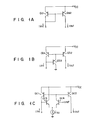
- Figs. l(a) to l(c) show prior art current mirror circuits.
- Fig. l(a) shows the proto-type current mirror circuit which has transistors Qal and Qa2 with their base-emitter paths connected in parallel.
- This circuit arrangement has a drawback in that an error of a comparatively large magnitude is provided between an input current Iin and an output current lout due to the base current of transistors Qal and Qa2 as is well known in the art.
- Fig. l(b) is an improved current mirror circuit which comprises a compensating transistor Qb3 of the complementary conductivity type to transistors Qbl and Qb2.
- the transistor Qb3 has its emitter connected to the bases of transistors Qbl and Qb2, its base connected to the collector of transistor Qbl and its collector connected to circuit ground. According to this circuit arrangement, the effect of the base current of transistors Qbl and Qb2 on the input current Iin can be reduced by a factor of the current amplification factor of transistor Qb3.
- a supply voltage at the input terminal supplied with the input current Iin must be lower than Vcc by the sum of the base-emitter voltages (about 0.7 volt in case of a silicon transistor) of transistors Qbl and Qb2.
- Fig. l(c) shows still another improved current mirror circuit.
- This circuit comprises emitter-coupled NPN transistors Qc3 and Qc4 in addition to current mirror PNP transistors Qcl and Qc2.
- Transistor Qc3 has its collector connected to a supply voltage Vcc and its base connected to the collector of transistor Qcl.
- transistor Qc4 has its collector connected to the bases of transistors Qcl and Qc2 and its base connected to a reference voltage Vref.
- the emitters of transistors Qc3 and Qc4 are connected through a current source of current value 10 to circuit ground.
- the current 10 is set to be higher than the sum of the base currents of transistors Qcl and Qc2.
- An object of the invention is to provide a current mirror circuit, in which the error between an input current and an output current is small, and which can be operated from a low supply voltage and is simple in construction.
- a current mirror circuit which comprises first and second transistors of a first conductivity type having their emitters each connected to a power supply, their bases connected together and their collectors respectively connected to an input terminal and an output terminal, and a third transistor of the first conductivity type having its emitter connected to the bases of the first and second transistors, its collector connected to a reference potential point and its base connected to the collector of the first transistor, a fourth transistor of a second conductivity type complementary to the first conductivity type is provided which has its collector connected to the power supply, its emitter connected to the base of the third transistor and its base connected to the collector of the first transistor, and a current source is connected between the base of the third transistor and the reference potential point.
- Fig. 2 shows a current mirror circuit embodying the invention.
- current mirror transistors Ql and Q2 of PNP type are provided with their emitters connected to a voltage source Vcc and their bases connected together.
- the collectors of transistors Ql and Q2 are respectively connected to an input terminal 11, supplied with an input current Iin and an output terminal 12 from which output current lout is led out.
- a PNP transistor Q4 is provided for current amplification factor compensation. This transistor Q4 has its emitter connected to the bases of transistors Ql and Q2 and its collector connected to a reference potential (circuit ground).
- An NPN transistor Q3 is provided for level shifting, which has its collector connected to voltage source Vcc, its emitter connected to the base of transistor Q4 and its base connected to the collector of transistor Ql. Between the base of transistor Q4 and circuit ground is connected a current source IS for providing current 10. The magnitude of 10 is set greater than the base current of transistor Q4.
- the current 10 of current source IS is set as follows: where ⁇ 1 is the current amplification factor of current mirror transistors Ql and Q2 and ⁇ 2 is the current amplification factor of transistor Q4.
- the current 10 of current source IS can be set 1/g lower than in the prior art circuit of Fig. l(c). This means that the base current of transistor Q3 which causes an error can be reduced.
- the voltage level at input terminal 11 may be lower than Vcc by the base-to-emitter voltage V BE of a single transistor (about 0.7 volt). This means that the current mirror circuit of the invention can be operated from a relatively low supply voltage.
- Fig. 3 shows another arrangement of the current mirror circuit of the invention in which a resistor R is connected between the emitter of transistor Q3 and the base of transistor Q4.
- the level shift voltage can be increased up to V BE + IOR. Namely, the voltage loss of this circuit becomes V BE - IOR and the loss voltage can be reduced to the level just prior to the saturation of first transistor Ql. Therefore, the circuit can be operated from a supply voltage lower than the circuit of Fig. 2.
- Fig. 4 shows still another arrangement of the invention in which a PNP transistor Q5 is provided for improving the linearity of the current mirror circuit by reducing the Early effect of transistor.
- Transistor Q5 has its emitter connected to the collector of transistor Q2, its collector connected to output terminal 12 and its base connected to the emitter of transistor Q3.
- the collector-emitter voltage V CE of transistor Q2 is 0.3 volt
- the bias current in a zero-signal condition 200 microamperes and the signal amplitude 100 microamperes the total harmonic distortion at 1 kHz was 0.1%.
- the total harmonic distortion is 3%.
Landscapes
- Engineering & Computer Science (AREA)
- Microelectronics & Electronic Packaging (AREA)
- Physics & Mathematics (AREA)
- Nonlinear Science (AREA)
- Electromagnetism (AREA)
- General Physics & Mathematics (AREA)
- Radar, Positioning & Navigation (AREA)
- Automation & Control Theory (AREA)
- Amplifiers (AREA)
Applications Claiming Priority (2)
| Application Number | Priority Date | Filing Date | Title |
|---|---|---|---|
| JP56091992A JPS57206107A (en) | 1981-06-15 | 1981-06-15 | Current mirror circuit |
| JP91992/81 | 1981-06-15 |
Publications (3)
| Publication Number | Publication Date |
|---|---|
| EP0067447A2 true EP0067447A2 (de) | 1982-12-22 |
| EP0067447A3 EP0067447A3 (en) | 1983-01-19 |
| EP0067447B1 EP0067447B1 (de) | 1986-03-26 |
Family
ID=14041934
Family Applications (1)
| Application Number | Title | Priority Date | Filing Date |
|---|---|---|---|
| EP82105236A Expired EP0067447B1 (de) | 1981-06-15 | 1982-06-15 | Stromspiegelschaltung |
Country Status (5)
| Country | Link |
|---|---|
| US (1) | US4462005A (de) |
| EP (1) | EP0067447B1 (de) |
| JP (1) | JPS57206107A (de) |
| CA (1) | CA1172711A (de) |
| DE (1) | DE3270079D1 (de) |
Cited By (8)
| Publication number | Priority date | Publication date | Assignee | Title |
|---|---|---|---|---|
| FR2546687A1 (fr) * | 1983-05-26 | 1984-11-30 | Sony Corp | Circuit miroir de courant |
| FR2547126A1 (fr) * | 1983-05-30 | 1984-12-07 | Sony Corp | Circuit convertiseur de tension en courant |
| US4766367A (en) * | 1987-07-20 | 1988-08-23 | Comlinear Corporation | Current mirror with unity gain buffer |
| EP0257345A3 (de) * | 1986-08-21 | 1989-04-26 | Tektronix Inc. | Kompensierter Stromspiegel |
| EP0299723A3 (en) * | 1987-07-17 | 1989-05-31 | Kabushiki Kaisha Toshiba | Current mirror circuit |
| EP0376471A1 (de) * | 1988-12-22 | 1990-07-04 | Delco Electronics Corporation | Niederverdrehungsstromspiegel |
| FR2679081A1 (fr) * | 1991-07-08 | 1993-01-15 | Matra Communication | Etage differentiel de courant a miroir de courant. |
| EP0530500A1 (de) * | 1991-07-31 | 1993-03-10 | Canon Kabushiki Kaisha | Stromspiegelschaltung |
Families Citing this family (20)
| Publication number | Priority date | Publication date | Assignee | Title |
|---|---|---|---|---|
| US4525682A (en) * | 1984-02-07 | 1985-06-25 | Zenith Electronics Corporation | Biased current mirror having minimum switching delay |
| JPS60244106A (ja) * | 1984-05-18 | 1985-12-04 | Oki Electric Ind Co Ltd | カレントミラ−回路 |
| JPH0623939B2 (ja) * | 1984-07-02 | 1994-03-30 | 沖電気工業株式会社 | カレントミラ−回路 |
| JPH0728184B2 (ja) * | 1985-06-24 | 1995-03-29 | 松下電器産業株式会社 | カレントミラー回路 |
| US5311146A (en) * | 1993-01-26 | 1994-05-10 | Vtc Inc. | Current mirror for low supply voltage operation |
| DE4302221C1 (de) * | 1993-01-27 | 1994-02-17 | Siemens Ag | Integrierbare Stromquellenschaltung unter Verwendung von bipolaren pnp-Transistoren |
| US5373253A (en) * | 1993-09-20 | 1994-12-13 | International Business Machines Corporation | Monolithic current mirror circuit employing voltage feedback for β-independent dynamic range |
| US5617056A (en) * | 1995-07-05 | 1997-04-01 | Motorola, Inc. | Base current compensation circuit |
| KR20010034225A (ko) | 1998-11-20 | 2001-04-25 | 롤페스 요하네스 게라투스 알베르투스 | 전류 미러 회로 |
| JP3232560B2 (ja) | 1999-01-21 | 2001-11-26 | 日本電気株式会社 | 位相比較回路 |
| US6842075B2 (en) * | 2001-06-06 | 2005-01-11 | Anadigics, Inc. | Gain block with stable internal bias from low-voltage power supply |
| US6753734B2 (en) | 2001-06-06 | 2004-06-22 | Anadigics, Inc. | Multi-mode amplifier bias circuit |
| US6515546B2 (en) | 2001-06-06 | 2003-02-04 | Anadigics, Inc. | Bias circuit for use with low-voltage power supply |
| US6507236B1 (en) * | 2001-07-09 | 2003-01-14 | Intersil Americas Inc. | Multistage precision, low input/output overhead, low power, high output impedance and low crosstalk current mirror |
| US6518832B2 (en) * | 2001-07-09 | 2003-02-11 | Intersil Americas Inc. | Mechanism for minimizing current mirror transistor base current error for low overhead voltage applications |
| JP2003124757A (ja) * | 2001-10-16 | 2003-04-25 | Texas Instr Japan Ltd | アーリー効果の影響を低減する方法および装置 |
| RU2307386C1 (ru) * | 2006-03-20 | 2007-09-27 | ГОУ ВПО "Южно-Российский государственный университет экономики и сервиса" (ЮРГУЭС) | Управляемый источник опорного напряжения |
| RU2362203C1 (ru) * | 2007-11-29 | 2009-07-20 | Государственное образовательное учреждение высшего профессионального образования "Южно-Российский государственный университет экономики и сервиса" (ГОУ ВПО "ЮРГУЭС") | Токовое зеркало |
| RU2396595C2 (ru) * | 2008-09-02 | 2010-08-10 | Государственное образовательное учреждение высшего профессионального образования "Южно-Российский государственный университет экономики и сервиса" (ГОУ ВПО "ЮРГУЭС") | Аналоговый перемножитель напряжений |
| RU2382484C1 (ru) * | 2008-12-02 | 2010-02-20 | Государственное образовательное учреждение высшего профессионального образования "Южно-Российский государственный университет экономики и сервиса" (ГОУ ВПО "ЮРГУЭС") | Аналоговый перемножитель напряжений |
Family Cites Families (4)
| Publication number | Priority date | Publication date | Assignee | Title |
|---|---|---|---|---|
| SE373248B (de) * | 1970-07-20 | 1975-01-27 | Rca Corp | |
| NL169239C (nl) * | 1971-10-21 | 1982-06-16 | Philips Nv | Stroomversterker. |
| US4237414A (en) * | 1978-12-08 | 1980-12-02 | Motorola, Inc. | High impedance output current source |
| JPS605085B2 (ja) * | 1980-04-14 | 1985-02-08 | 株式会社東芝 | カレントミラ−回路 |
-
1981
- 1981-06-15 JP JP56091992A patent/JPS57206107A/ja active Granted
-
1982
- 1982-06-11 US US06/387,750 patent/US4462005A/en not_active Expired - Lifetime
- 1982-06-14 CA CA000405097A patent/CA1172711A/en not_active Expired
- 1982-06-15 DE DE8282105236T patent/DE3270079D1/de not_active Expired
- 1982-06-15 EP EP82105236A patent/EP0067447B1/de not_active Expired
Cited By (11)
| Publication number | Priority date | Publication date | Assignee | Title |
|---|---|---|---|---|
| FR2546687A1 (fr) * | 1983-05-26 | 1984-11-30 | Sony Corp | Circuit miroir de courant |
| GB2146501A (en) * | 1983-05-26 | 1985-04-17 | Sony Corp | Current mirror |
| FR2547126A1 (fr) * | 1983-05-30 | 1984-12-07 | Sony Corp | Circuit convertiseur de tension en courant |
| GB2142794A (en) * | 1983-05-30 | 1985-01-23 | Sony Corp | Voltage to current converting circuit |
| EP0257345A3 (de) * | 1986-08-21 | 1989-04-26 | Tektronix Inc. | Kompensierter Stromspiegel |
| EP0299723A3 (en) * | 1987-07-17 | 1989-05-31 | Kabushiki Kaisha Toshiba | Current mirror circuit |
| US4766367A (en) * | 1987-07-20 | 1988-08-23 | Comlinear Corporation | Current mirror with unity gain buffer |
| EP0376471A1 (de) * | 1988-12-22 | 1990-07-04 | Delco Electronics Corporation | Niederverdrehungsstromspiegel |
| FR2679081A1 (fr) * | 1991-07-08 | 1993-01-15 | Matra Communication | Etage differentiel de courant a miroir de courant. |
| EP0530500A1 (de) * | 1991-07-31 | 1993-03-10 | Canon Kabushiki Kaisha | Stromspiegelschaltung |
| US5283537A (en) * | 1991-07-31 | 1994-02-01 | Canon Kabushiki Kaisha | Current mirror circuit |
Also Published As
| Publication number | Publication date |
|---|---|
| EP0067447B1 (de) | 1986-03-26 |
| JPH027522B2 (de) | 1990-02-19 |
| US4462005A (en) | 1984-07-24 |
| EP0067447A3 (en) | 1983-01-19 |
| DE3270079D1 (en) | 1986-04-30 |
| CA1172711A (en) | 1984-08-14 |
| JPS57206107A (en) | 1982-12-17 |
Similar Documents
| Publication | Publication Date | Title |
|---|---|---|
| EP0067447A2 (de) | Stromspiegelschaltung | |
| JPS6245724B2 (de) | ||
| KR900008752B1 (ko) | 전류미러회로 | |
| EP0155720B1 (de) | Kaskadenstromquellenanordnung | |
| JPH0446009B2 (de) | ||
| KR970005292B1 (ko) | 차동증폭회로 | |
| KR930007295B1 (ko) | 증폭기 장치 | |
| US4937515A (en) | Low supply voltage current mirror circuit | |
| EP0155039B1 (de) | Stromquellenkreis | |
| KR930001292B1 (ko) | 푸시-풀 증폭기 | |
| US4217555A (en) | Amplifier circuit arrangement with stabilized power-supply current | |
| US6734720B2 (en) | Operational amplifier in which the idle current of its output push-pull transistors is substantially zero | |
| US4403200A (en) | Output stage for operational amplifier | |
| US4928073A (en) | DC amplifier | |
| CA1208313A (en) | Differential amplifier | |
| KR930007294B1 (ko) | 달링턴 트랜지스터 장치 | |
| US5285170A (en) | Operational amplifier with all NPN transistor output stage | |
| EP0104777B1 (de) | Schaltung für Konstantstromquelle | |
| US4553107A (en) | Current mirror circuit having stabilized output current | |
| JPS6154286B2 (de) | ||
| US6255868B1 (en) | Buffer circuit and hold circuit | |
| JPH0362042B2 (de) | ||
| KR900008754B1 (ko) | 차동증폭회로 | |
| KR850000581B1 (ko) | 신호 변환 회로 | |
| JP2547896B2 (ja) | 電流反転回路 |
Legal Events
| Date | Code | Title | Description |
|---|---|---|---|
| PUAI | Public reference made under article 153(3) epc to a published international application that has entered the european phase |
Free format text: ORIGINAL CODE: 0009012 |
|
| PUAL | Search report despatched |
Free format text: ORIGINAL CODE: 0009013 |
|
| 17P | Request for examination filed |
Effective date: 19820615 |
|
| AK | Designated contracting states |
Designated state(s): DE FR GB |
|
| AK | Designated contracting states |
Designated state(s): DE FR GB |
|
| RAP1 | Party data changed (applicant data changed or rights of an application transferred) |
Owner name: KABUSHIKI KAISHA TOSHIBA |
|
| GRAA | (expected) grant |
Free format text: ORIGINAL CODE: 0009210 |
|
| AK | Designated contracting states |
Kind code of ref document: B1 Designated state(s): DE FR GB |
|
| ET | Fr: translation filed | ||
| REF | Corresponds to: |
Ref document number: 3270079 Country of ref document: DE Date of ref document: 19860430 |
|
| REG | Reference to a national code |
Ref country code: GB Ref legal event code: 746 |
|
| PLBE | No opposition filed within time limit |
Free format text: ORIGINAL CODE: 0009261 |
|
| STAA | Information on the status of an ep patent application or granted ep patent |
Free format text: STATUS: NO OPPOSITION FILED WITHIN TIME LIMIT |
|
| 26N | No opposition filed | ||
| REG | Reference to a national code |
Ref country code: FR Ref legal event code: D6 |
|
| PGFP | Annual fee paid to national office [announced via postgrant information from national office to epo] |
Ref country code: FR Payment date: 20010611 Year of fee payment: 20 Ref country code: DE Payment date: 20010611 Year of fee payment: 20 |
|
| PGFP | Annual fee paid to national office [announced via postgrant information from national office to epo] |
Ref country code: GB Payment date: 20010613 Year of fee payment: 20 |
|
| REG | Reference to a national code |
Ref country code: GB Ref legal event code: IF02 |
|
| PG25 | Lapsed in a contracting state [announced via postgrant information from national office to epo] |
Ref country code: GB Free format text: LAPSE BECAUSE OF EXPIRATION OF PROTECTION Effective date: 20020614 |
|
| REG | Reference to a national code |
Ref country code: GB Ref legal event code: PE20 Effective date: 20020614 |