EP0155781B1 - Appareil détecteur de coordonnées - Google Patents
Appareil détecteur de coordonnées Download PDFInfo
- Publication number
- EP0155781B1 EP0155781B1 EP85301314A EP85301314A EP0155781B1 EP 0155781 B1 EP0155781 B1 EP 0155781B1 EP 85301314 A EP85301314 A EP 85301314A EP 85301314 A EP85301314 A EP 85301314A EP 0155781 B1 EP0155781 B1 EP 0155781B1
- Authority
- EP
- European Patent Office
- Prior art keywords
- detecting apparatus
- coordinate
- coordinate detecting
- diodes
- resistive film
- Prior art date
- Legal status (The legal status is an assumption and is not a legal conclusion. Google has not performed a legal analysis and makes no representation as to the accuracy of the status listed.)
- Expired
Links
Images



Classifications
-
- G—PHYSICS
- G06—COMPUTING OR CALCULATING; COUNTING
- G06K—GRAPHICAL DATA READING; PRESENTATION OF DATA; RECORD CARRIERS; HANDLING RECORD CARRIERS
- G06K11/00—Methods or arrangements for graph-reading or for converting the pattern of mechanical parameters, e.g. force or presence, into electrical signal
-
- G—PHYSICS
- G06—COMPUTING OR CALCULATING; COUNTING
- G06F—ELECTRIC DIGITAL DATA PROCESSING
- G06F3/00—Input arrangements for transferring data to be processed into a form capable of being handled by the computer; Output arrangements for transferring data from processing unit to output unit, e.g. interface arrangements
- G06F3/01—Input arrangements or combined input and output arrangements for interaction between user and computer
- G06F3/03—Arrangements for converting the position or the displacement of a member into a coded form
- G06F3/041—Digitisers, e.g. for touch screens or touch pads, characterised by the transducing means
- G06F3/045—Digitisers, e.g. for touch screens or touch pads, characterised by the transducing means using resistive elements, e.g. a single continuous surface or two parallel surfaces put in contact
-
- G—PHYSICS
- G06—COMPUTING OR CALCULATING; COUNTING
- G06F—ELECTRIC DIGITAL DATA PROCESSING
- G06F3/00—Input arrangements for transferring data to be processed into a form capable of being handled by the computer; Output arrangements for transferring data from processing unit to output unit, e.g. interface arrangements
- G06F3/01—Input arrangements or combined input and output arrangements for interaction between user and computer
- G06F3/03—Arrangements for converting the position or the displacement of a member into a coded form
Definitions
- the present invention relates to a coordinate detecting apparatus.
- a so-called soft key is a coordinate data inputting means comprising an input panel stacked on (mounted over) the surface of a display device which permits the input of the coordinates of a point on the panel simply by applying a touch of a fingertip, etc, to the panel.
- the soft key can greatly facilitate the man- machine interaction in a computer system. For example, the selection of a menu on a display device or inputting of a pattern to a computer system can be performed not using a keyboard but only touching the input panel or writing the pattern on the panel. Exemplary application of such a soft key has been realized in a window machine for banks or a seat reservation terminal for travel agencies. The use of the soft-key is expected to increase more and more according to the trend toward the society of integrated digital information networks where easy-to-operate terminals for nonspecialized persons are essential.
- a previously proposed coordinate data inputting technology for a soft key as described above involves a ditital type apparatus comprising a plurality of sensors disposed to form a matrix arrangement on a plane. By indicating one or more of the sensors with a touch of a fingertip or pen, coordinate data corresponding to the position(s) of the sensor(s) is input to a control unit.
- detection accuracy in the coordinate data obtained by using such digital type means depends on the number of sensors per inch, and may be insufficient for applications requiring high resolution necessary for inputting a fine or complicated pattern.
- Fig. 1 is a circuit block diagram of a conventional coordinate detecting apparatus of the aforesaid analog type.
- an output terminal 5 of a voltage source 8 is connected to an end 2 of a uniform resistive film 1 via a current measuring means 9.
- the output terminal 5 of the voltage source 8 is also connected to another end 3 of the resistive film 1 via another current measuring means 10.
- Another output terminal of the voltage source 8 is connected to the ground 7.
- the output of the current measuring means 9 is connected to an analog-to-digital converter (ADC) 11, while the output of the current measuring means 10 is connected to another ADC 12.
- ADC analog-to-digital converter
- the outputs of both ADCs 11 and 12 are individually connected to a control unit 13.
- the resistance between arbitrary two points on the resistive film 1 is proportional to the distance between the points.
- the coordinate x of an arbitray point 4 on the resistive film 1 is represented by the equation where, 0 ⁇ x ⁇ 1, and, Rx and R i - x denote respective resistances between the end 2 and point 4 and between the end 3 and point 4.
- I X and I 1-x denote respective currents flowing through the ends 2 and 3.
- equation (1) can be represented as follows: and thus, the coordinate of the point 4 can be determined by the currents I x and I,_ x , both measured by using the current measuring means 9 and 10.
- the values of the curernts I x and h 1-x are converted to corresponding digital data by the respective ADCs 11 and 12, and processed by the control unit 13 to provide digital coordinate data, according to equation (3).
- the conventional coordinate detecting apparatus shown in Fig. 1 uses current measuring means 9 and 10, each of which usually comprise an operational amplifier serving to provide a voltage output signal corresponding to the measured current.
- the coordinate detecting apparatus also requires analog-to-digital converters (ADCs) 11 and 12 of high quantization accurancy. As a result, the apparatus inevitably has a complicated circuit configuration and high cost.
- ADCs analog-to-digital converters
- WO-80/01762 discloses a touch panel system and method for detecting a co-ordinate of a point on a resistive film, in which the ends of the resistive film are connected to the inverting inputs of respective operational amplifiers.
- a signal generator is connected in common to the non-inverting inputs of the operational amplifiers, and a respective subtractor is connected between the non-inverting input and output of each operational amplifier.
- the subtractors are connected to respective rectifier circuits whose outputs are connected to an adder and divider arrangement for producing a co-ordinate signal.
- US-A-4,103,252 discloses a capacitive touch- activated transducer system including an RC network as part of an oscillator.
- a human touch on a copper electrode produces a capacitive change, altering the RC time constant and thus changing the frequency of the output signal of the oscillator.
- Four copper electrodes may be arranged to enable sensing of position along two orthogonal axes simultaneously.
- an apparatus for detecting a co-ordinate of a point on a resistive film comprising:
- An embodiment of the present invention can provide a coordinate detecting apparatus comprising simple circuitry.
- An embodiment of the present invention can provide a coordinate detecting apparatus of low cost.
- An embodiment of the present invention can also provide a coordinate detection apparatus having a high detecting accuracy.
- An embodiment of the present invention can also provide a coordinate detecting apparatus which can be used as a soft key for a computer input device when stacked on a display device.
- An embodiment of the present invention can provide an analog type apparatus using a resistive film constituting a plane on which a position of a point whose coordinate is to be detected is indicated by applying a load impedance to the position.
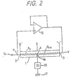
- Fig. 2 is a circuit block diagram used for explaining the principle of the present invention. Unlike in the conventional apparatus shown in Fig. 1, ends 2 and 3 of a resistive film 1 are not connected to a voltage source; rather, the end 2 is connected to a terminal 14 and the end 3 is connected to the end 2 via a buffer circuit, for example, an operational amplifier (referred to as op amp, hereinafter) 15 used in a voltage follower mode. More specifically, the end 2 is connected to the non-inverting input (+) of the op amp 15, and the output of the op amp 15 is connected to its inverting input (-) together with the end 3.
- op amp operational amplifier
- the ends 2 and 3 of the resistive film 1 are made to have an equal potential with respect to the ground 17.
- the input impedance of the op amp 15 can be assumed to be infinite, therefore, the current flowing through the terminal 14 does not include a current component flowing from the end 3 to a point 4 on the resistive film 1, even when a load 16 is applied to the point 4.
- the potential at the ends 2 and 3 with respect to the ground 17 is represented by V
- the potential at the point 4 with respect to the ground 17 is represented by Va
- the impedance between the terminal 14 and ground 17 is represented by Z.
- the impedance Z involves the respective resistances R x between the end 2 and point 4 and R,- x between the end 3 and point 4, and a load impedance Zo between the point 4 and ground 17, and is, therefore, referred to hereinafter as an equivalent impedance.
- the coordinate x of an arbitrary point 4 on the resistive film 1 is given as a function of the equivalent impedance Z.
- the value of the equivalent impedance Z can be derived as follows.
- a current flowing through the load impedance Zo which current may be expressed as Va/Zo, is equal to the sum of the current flowing through R x and the current flowing through R 1-x .
- the currents flowing through R x and R i - x may be expressed as (V-Va)/R x and (V-Va)/R 1-x , respectively.
- the current flowing through the terminal 14 does not include the current flowing through R,- x . Therefore, the current flowing through the equivalent impedance Z, which current may be expressed as V/Z, may be taken as equal to the current flowing through R x , that is:
- equation (6) can be approximated as follows:
- the coordinate x of a point on the resistive film 1 is given by accordingly, by combining equations (8) and (7), the equation representing the coordinate x as a function of the equivalent impedance Z is derived as follows.
- the coordinate x can be determined according to equation (9).
- both ends of the resistive film 1 are connected to each other via a buffer circuit operating in a voltage follower mode, and the equivalent impedance Z of the terminal 14 with respect to the ground 17 is measured when a load impedance Zo is applied to an arbitrary point 4 on the resistive film 1.
- the impedance Zo is selected to be sufficiently larger than the resistance of the resistive film 1.
- the coordinate x of the point 4 on the resistive film 1 is calculated by substituting the impedance data in equation (9).
- the equivalent impedance Z between the terminal 14 and ground 17 may be considered to be composed of an equivalent capacitance expressed as follows:
- the equivalent impedance Z between the terminal 14 and ground 17 can be considered as an equivalent capacitance, and the coordinate x is determined by measuring relevant capacitances C and Co.
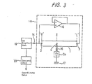
- Fig. 3 illustrates an exemplary circuit configuration embodying a coordinate detecting apparatus based on the principle explained with reference to Fig, 2, as a first embodiment of the present invention in this embodiment a capacitance Co of the load 16 applied to an arbitrary point 4 on the resistive film 1, and the equivalent capacitance C between the terminal 14 and ground 17, are respectively measured to determine the coordinate x of the point 4 according to equation (13).
- the configuration and operation of those parts of the apparatus, enclosed by the broken line 100 are the same as explained with reference to the corresponding part in Fig. 2.
- a capacitance measuring means for example, a CR digital oscillator 19, is connected to the terminal 14, and the output of the CR digital oscillator 19 is connected to the input of a control unit 20.
- the CR digital oscillator 19 outputs pulses of a frequency corresponding to the time constant determined by the values of external resistor and capacitance connected to it.
- the repetition period of the pulses output from the oscillator 19 is proportional to the equivalent capacitance C.
- the control unit 20 determines the repetition period of input pulses by its built-in timer and calculates the value of the coordinate x of the point 4 according to equation (9) or (13).
- the CR digital oscillator 19 may comprise an astable multivibrator, such as NE555 marketed by Sygnetics Inc., for example.
- An input pen having a capacitance of about 1000 pF, for example, may be used for the load impedance 16.
- An internal clock pulse of about 6 MHz may be used for the aforesaid timer in the control unit 20, and therefore, the CR digital oscillator 19 is set to operate in a frequency range of tens of kHz or less.
- a resistive film 1 having a sheet resistance in the range from 200 to 500 ohms may generally be employed.
- the load impedance provided by the 1000 pF input pen is in a range around 5 to 15 kilohms. This impedance is ten times or more larger than the resistance of the resistive film 1 and can comply with the assumption used for deriving the equation (7).
- a constant k may be introduced for establishing a relationship between the repetition period of the output pulses and input capacitance of the oscillator 19. That is, where, To denotes the repetition period obtained when the capacitance at the terminal 14 is Co, and T denotes the repetition period obtained when the capacitance at the terminal 14 is C.
- the equation (13) expressing the coordinate x as a function of the capacitances Co and C is modified as follows:
- the coordinate x is determined by measuring the respective repetition periods corresponding to the load capacitance Co and equivalent capacitance C.
- the equivalent capacitance C is measured by applying the load capacitance Co to the point 4 whose coordinate x is to be detected.
- the data corresponding to the respective repetition periods To and T are stored in the memory of the control unit 20, and then, processed for providing the coordinate value x of the point, according to the formula (16).
- the CR digital oscillator 19 is commercially available at a low cost, and the control unit 20 can be comprised of a conventional timer, arithmetic device and latching circuit, all of which are also commercially available at low cost.
- the coordinate detecting apparatus of this embodiment of the present invention can be provided at a lower cost compared with the conventional apparatus at shown in Fig. 1, without any sacrifice of operational reliability.
- the input panel of the coordinate detecting apparatus shown in Fig. 3 can be directly superimposed upon (stacked on) the surface of a display device, and used in applications such as a touch panel for inputting a selected menu on the display, wherein the selected menu is indicated by applying a fingertip touch on the input panel.
- the coordinate detecting apparatus shown in Fig. 3 uses the variation of the equivalent capacitance C between the end of the resistive film 1 and the ground 17 in accordance with the application of the load capacitance Co, the surface of the resistive film 1 may be coated by an insulating film for protection against mechanical wear or scratching.
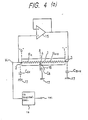
- Figs. 4(a) and 4(b) are circuit configurations for explaining the principle of a second embodiment of the present invention. Based on the same principle as explained with reference to Fig. 2, this embodiment permits to determine a coordinate x on an input panel to be determined using a load impedance having an unknown value. That is, in this embodiment, it is not necessary to measure the value of the load impedance. In other words, this embodiment is intended to provide a coordinate detecting apparatus substantially operable with the use of a load impedance whose value is unstable.
- the load impedance i.e. the capacitance Co
- the capacitance Co is supposed to be constant during a sequence from the time when an input pen touches the end 2 for determining the value Co to the time when the input pen touches the position of an arbitrary point 4 on the resistive film 1.
- the sequence will take some seconds at least in a practical operation.
- To keep the load capacitance Co constant is easy if an input pen is used for indicating the point, but difficult if a touch of a fingertip is used instead of an input pen, because the load capacitance Co applied by a human body through a fingertip is apt to change with the contact pressure of a fingertip to the resistive film 1 and also with operator's sitting posture, for example.
- the ends 2 and 3 have respective stray capacities with respect to the ground 17, in general. If the stray capacities are too large to be neglected, it is necessary to correct the equivalent capacitance C measured at the terminal 14 for the stray capacities.
- a load capacitance (represented by C B ) is required constant only in very short time and is excluded from the process of the coordinate detection. Therefore, the load capacitance may be such one which fluctuates and has an unknown value as a floating capacity of a human body to the ground 17.
- Equation (14) includes the stray capacity C Sx which stands in parallel to the equivalent capacitance C xi .
- the stray capacity Cs i - x has been neglected because the end 3 is connected to the output of the op amp 15 whose output impedance can be assumed to be substantially zero.
- the CR digital oscillator 19 connected to the end 2 via the terminal 14 outputs signal pulses having a repetition period proportional to the equivalent capacitance C x1 .
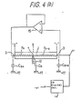
- Fig. 4(b) illustrates a situation where the respective connections of the input and output of the op amp 15 to the ends 2 and 3 are exchanged, and the CR digital oscillator 19 is connected to the end 3 via a terminal 21. If the change of the connections between Fig. 4(a) and Fig. 4(b) is carried out in a very short time, for example, 5 ms, the fluctuation of the capacitance C B (during the change) is negligibly small. Hence, in the configuration of Fig.
- Equation (15) includes the stray capacity C S1-x which exists in parallel to the equivalent capacitance C x2 . This time, the stray capacity Cs x at the end 2 has been neglected because in this situation, the end 2 is connected to the output of the op amp 15 having an output impedance of substantially zero.
- the coordinate detection of the second embodiment is performed according to equation (17). That is, the coordinate detecting apparatus of the second embodiment comprises switching means, permitting switching of the connections of the circuit to the resistive film 1 from the situation shown in Fig. 4(a) to that shown in Fig. 4(b) in a very short time and measuring means for meas- ruing the respective equivalent capacitance C x1 between the terminal 14 and the ground 17 and C x2 between the terminal 21 and ground 17 and the respective stray capacities Csx at the end 2 and C 1-x at the end 3, in accordance with the operation of the switching means.
- the coordinate x of the point 4, to which a load capacitance C B constiting of a floating capacity of a human body is applied by, for example a fingertip 18, is determined by substituting the measured values of these capacitances C x1, C X2 , Csx and C 1-x for the respective terms in equation (17).
- the repetition period of pulses output from the terminal 191 of the CR digital oscillator 19 is proportional to the equivalent capacitance between the terminal 14 or 19 and the ground 17.
- the repetition period T x1 of the output pulses in the configuration shown in Fig. 4(a) is given by where, k is a constant.
- the equivalent capacitances C x , and C x2 are detected as the repetition periods of respective output pulses from the terminal 191, as expressed by equations (18) and (19).
- the stray capacity C s1-x is given as the equivalent capacitance C X2 without touching the fingertip 18 to the resistive film 1 of Fig. 4(b), and repetition period Ts l - x of the output pulses from the terminal 191 is expressed by where, C' s1-x designates the relevant equivalent capacitance between the terminal 21 and ground 17.
- the respective repetition periods in both situations shown in Figs. 4(a) and 4(b) are measured without application of a touch of the fingertip 18, and then, during a touch of the of the fingertip 18 is applied to the resistive film 1.
- the coordinate of the point 4 indicated by the touch of the fingertip 18 is determined by substituting the values of the repetition periods measured according to equations (18), (19), (20) and (21) for the respective terms in equation (22) instead of corresponding equation (17) in which the coordinate is given by the respective capacitances.
- a feature of this embodiment is the switching operation performed in a very short time between the circuits of Figs. 4(a) and 4(b).
- Fig. 5 illustrates a circuit configuration of the third embodiment of the coordinate detecting apparatus according to the present invention, wherein 2-dimensional coordinate detection is made possible.
- an input panel (referred to as a touch panel, hereinafter) 22 has a structure comprising a transparent resistive film formed on a glass substrate and coated with an insulating thin film such as Si0 2 .
- the left end of the touch panel 22 is connected to a common line L 1 by switching lines A x" , A x12 ,...A x1m of an analog switch array 22.
- the right end of the touch panel 22 is connected to another common line L 2 by switching lines A x21, A x22, ...A x2m of a second analog switch array 24.
- the top end of the touch panel 22 is connected to the common line L 1 by switching lines Ay 11, A y12, ...A y1n of a third analog switch array 25.
- the bottom end of the touch panel 22 is connected to the common line L 2 by switching lines Ay 2 ,, Ay 22 ,...Ay 2n of a fourth analog switch array 26.
- Each of the analog switch arrays 23, 24, 25 and 26 is referred to as second switching means.
- the respective control signal inputs of the analog switches 23 and 24 are connected to a control signal line H 1 linked to a control unit 20, and the respective control signal inputs of the analog switches 25 and 26 are connected to the control signal line H 1 via respective inverters 31 and 32.
- the common line L is connected to a terminal S, of first switching means 27, and the terminal S 1 is selectively connected to terminals 1 1 and O 1 .
- the common line L 2 is connected to the terminal S 2 of the first switching means 27, and a terminal S 2 is selectively connected to terminals 1 2 an 0 2 .
- the first switching means 27 may be an analog switching means, for example, comprising a couple of transfer contacts as shown in Fig. 5.
- the control signal input of the first switching means 27 is connected to another control signal line H 2 linked to the control unit 20.
- the non-inverting input of op amp 15 is connected to the terminals I 1 , and 1 2 of the switching means 27 and also connected to a capacitor terminal of a CR digital oscillator 19.
- the inverting input and the output of the op amp 15 are connected to each other, and also connected to the terminals 0, and 0 2 of the switching means 27.
- the output of the CR digital oscillator 19 is connected to the input of control unit 20 which outputs the detected coordinate data on its output terminal 34.
- the point whose coordinate on the touch panel 22 is to be detected is indicated by touching the fingertip 18 to the point.
- the point is applied with a load capacitance C B provided by a floating capacity of a human body with respect to the ground 17.
- the capacitance C B involves the capacitive component relating to the Si0 2 film on the resistive film 1.
- the analog switch arrays 23, 24, 25 and 26 operate to alternately establish a current path between the left end and right end of the touch panel 22 (i.e. the current path in X direction) and between the top end and bottom end of the touch panel 22 (i.e. the current path in Y direction).
- the analog switch arrays 23 and 24 are closed, the analog switch arrays 25 and 26 are opened.
- the op amp 15 constitutes a voltage follower circuit. The respective connections of the input and output of the op amp 15 to the common lines L, and L 2 are exchanged by the first switching means 27 according to the signal on the control signal line H 2 .
- a high level signal for example, is output from the control unit 20 to the control signal line H 1, and hence, the analog switch arrays 23 and 24 are closed, while the analog switch arrays 25 and 26 are opened due to the supply of a low level signal by the inverters 31 and 32.
- a current path is established in the X direction.
- a high level signal for example, is output from the control unit 20 and applied to the first switching means 27 via the control signal line H 2 .
- the terminal S 1 is connected to the terminal I 1
- the terminal S 2 is connected to the terminal 0 2 .
- the CR digital oscillator 19 outputs signal pulses of repetition period T x1 corresponding to the equivalent capacitance C X1 . between the left end of the touch panel 22 and the ground 17.
- the repetition period T x1 is measured by a timer, and then, stored in a memory, both of the timer and memory are built in the control unit 20.
- the repetition period Ts x corresponding to the stray capacity Cs x at the left end of the touch panel 22 is measured without application of the touch of the fingertip 18, and stored in the memory, in advance.
- the signal output from the control unit 20 to the control signal line H 2 turns to low level, and the switching means 27 operates to connect the terminal S 1 to the terminal O 1, and the terminal S 2 to the terminal 1 2 .
- the signal on the control signal line H 1 remains at a high level to maintain the current path in the X direction. Accordingly, the connection between the op amp 15 and the touch panel 22 becomes equivalent to the circuit shown in Fig. 4(b).
- the CR digital oscillator 19 outputs signal pulses of repetition period T x2 corresponding to the equivalent capacitance C x2 between the right end of the touch panel 22 and the ground 17.
- the repetition period of T X2 is measured by the timer, and then, stored in the memory of the control unit 20.
- the repetition period Ts 1-x corresponding to the stray capacity C S1-x at the right end of the touch panel 22 is measured without the application of the touch of the fingertip 18, and stored in the memory, in advance.
- an arithmetic processor in the control unit 30 performs operation according to equation (22), and thus, the coordinate in the left to right direction, i.e. X coordinate, of the point indicated by the touch of the fingertip 18 to the touch panel 22 is detected, and then, output from the terminal 34.
- the coordinate of the left end of the touch panel 22 is defined as "0" and the coordinate of the right end is defined as "1" .
- the signal output from the control unit 20 to the control signal line H is turned to low level, and the analog switch arrays 25 and 26 are closed, while the analog switch arrays 23 and 24 are opened.
- the current path is changed from the left and right direction to the top and bottom direction, i.e. Y direction, and the Y coordinate of a point indicated by the touch of the fingertip 18 is detected in the same manner as in the X coordinate detection as described above.
- the coordinate of the top end of the touch panel 22 is defined as "0" and the coordinate of the bottom end is defined as "1".
- a high precision 2-dimensional coordinate value of a point indicated by the touch of the fingertip 18 to the touch panel 22 can be determined.
- the switching operation of the switching means 27 according to the signal on the control signal line H 2 is performed every very short time interval, 1 ms, for example, and operation of the analog switches 23, 24, 25 and 26 according to the control signal H, performed every 2 ms, for example.
- the load capacitance C B provided by a floating capacity of a human body is supposed to be constant during a short time such as 5 ms.
- the coordinate of a point on the touch panel 22 is determined according to a statistical process based on the values obtained during plural successive measurements.
- coordinate x is determined as follows:
- the control unit 20 outputs the value of the coordinate x from the output terminal 34 after every f measurements.
- the same process may be performed for the detection of a y coordinate.
- the analog switches 23, 24, etc. and the device for the switching means 27 are commercially available at low costs, therefore, the total cost of the coordinate detecting apparatus of the second, third or fourth embodiment of the present invention can also, be lower than the conventional apparatus as shown in Fig. 1.
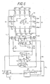
- Fig. 6 illustrates a fifth embodiment of the present invention.
- This embodiment is a modification of the embodiment shown in Fig. 5, and comprises a diode array, biasing means and bias switching means.
- the diode array constitutes the second switching means, instead of the analog switches 23,24,25 and 26 in the previous embodiment.
- each end (edge) of the touch panel 22 is provided with a diode array; a diode array 35 comprising diodes D x1, D x2 , D x3 ,... for the left end; a diode array 36 comprising diodes D x1 ,., D x2 ', Dx3'... for the right end; a diode array 37 comprising diodes Dy 1, Dy 2 , Dy 3 ... for the top end; diode array 38 comprising diodes D Y1 ,, D Y2 ', Dy3; for the bottom end.
- the diodes in the diode arrays 35 and 36 are arranged to have a common forward direction
- the diodes in the diode arrays 37 and 38 are arranged to have a common forward direction. That is, for example, the diodes D x1 , DX 2 , D x3, .... are connected to the touch panel 22 through their cathodes, while the diodes D x1 , , D x2 ,, D x3 , ... are connected to the touch panel 22 through their anodes.
- the diodes Dy,, Dy 2, Dy 3 ... are connected to the touch panel 22 through their anodes, while the diodes Dy 1 , , D Y2 , , Dy 3 '.... are connected to the touch panel 22 through their cathodes.
- the anodes of the diodes D x1 , D x2, D x3 ,... are connected to a common line L 1 together with the cathodes of the diodes Dy 1 , D Y21 Dy 3 ..., while the cathodes of the diodes D x1', D x2 , , D x3 ,... are connected to another common line L 2 together with the anodes of the diodes Dy 1 , , D Y2' , Dy 3 ,....
- a bias voltage Eo is applied via bias switching means 39 having terminals p1, p2, q1, q2, r1 and r2.
- the terminal p1 is connected to the common line L, via serially connected resistors R 1 and R 2
- the terminal p2 is connected to the common line L 2 via other serially connected resistors R 3 and R 4
- the terminals q1 and r2 are connected to the ground 17 and the terminals r1 and q2 of the bias switching means 39 are connected to a DC voltage source Eo referred to as a biasing means, wherein the terminal p1 is selectively connected to the terminals q1 and r1 and the terminal p2 is selectively connected to the terminals q2 and r2, according to the signal provided by the control unit 20 via the control signal line H 1 .
- Capacitors C, and C 2 are respectively connected to the node of the resistors R 1 and R 2 and the node of the resistors R 3 and R 4 .
- the respective opposite ends of the capacitors C, and C 2 are commonly connected to the output of the op amp 15.
- the non-inverting input of the op amp 15 is connected to the CR digital oscillator 19 via a capacitor C 4 .
- the first switching means 27' is substantially equivalent to the first switching means 27 in Fig. 5, however, its connection to the output of the op amp 15 is intercepted by a capacitor C 3 .
- the terminal S 1 is selectively connected to the terminals 1 1 and O 1
- the terminal S 2 is selectively connected to the terminals 0 2 and 1 2 , according to the signal provided by the control unit 20 via the control signal line H 2 .
- the bias switching means 39 operates to respectively connect the terminals p1 and p2 to the terminals r1 and r2, according to the signal from the control unit 20 via the control signal line H 1 .
- the DC bias voltage Eo 12 volts, for example, is applied to the common line L, via the resistors R 2 and R 1 , and biases the diodes in the diode array 35 in forward direction and the diodes in the diode array 37 in reverse direction.
- the common line L 2 is connected to the ground 17 via the resistors R 4 and R 3 , accordingly, the diodes in the diode array 36 are biased in forward direction, and thus, a current path is established in the X direction on the touch panel 22.
- the potential on the common line L is higher than that on the common line L 2 , therefore, the diodes in the diode array 38 are biased in reverse direction and substantially made to be in the open state. Accordingly, current can not flow from the diode array 38 to the diode array 37 on the touch panel 22.
- the first switching means 27' operates to connect the input and output of the op amp 15 to the common lines L, and L 2 , respectively, and then, operates to exchange the respective connections of the input and output of the op amp 15 to the common lines L, and L 2 , according to the signal on the control signal lines H 2 .
- the repetition periods T x1, T x2, Ts x and Ts 1-x of the oputput pulses from the CR digital oscillator 19 are measured and stored by the control unit 20, and the coordinate x of the point indicated by applying a touch of the fingertip 18 is determined according to equation (22) or (23) as described with reference to Fig. 5.
- the bias switching means 39 operates to switch the terminals p1 and p2 to the terminals q1 and q2, respectively, according to the change of the signal on the control signal line H 1 .
- the common line L 1 is connected to the ground 17 via the resistors R 1 and R 2
- the common line L 2 is connected to the bias voltage source Eo via the resistors R 3 and R 4 .
- the diodes in the diode array 38 are biased in forward direction and the diodes in the diode array 36 are biased in reverse direction.
- the common line L 1 is connected to the ground 17 via the resistors R 1 and R 2 , and the diodes in diode array 37 are biased in forward direction, and thus, a current path is established in the Y direction.
- the potenital on the common line L 2 is higher than that of the common line L 1 , therefore, the diodes in the diode array 35 are biased in reverse direction, and substantially placed in the open state. Accordingly, current can not flow from the diode array 35 to the diode array 36 on the touch panel 22.
- the first switching means 27' operates to exchange the respective connections of the input and output of the op amp 15 to the common lines L, and L 2 , according to the signal on the control signal line H 2 , and coordinate y of the point indicated by the touch of the fingertip 18 is determined according to the same procedure as in the detection of the coordinate x.
- Fig. 7 illustrates the sixth embodiment of the present invention. This embodiment is a modification of the previous embodiment shown in Fig. 6, and is intended to improve the operation speed of the previous embdopiment.
- the circuit of the coordinate detecting apparatus of Fig. 6 is provided with the capacitors C 1, C 2 , C 3 and C 4 , each having a relatively large capacitance such as 0.1 ⁇ F.
- the capacitor C 3 is for blocking the DC bias voltage Eo to flow (from being applied) from the common line L, or L 2 to the ground 17 through the output of the op amp 15 having a low output impedance substantially zero.
- the capacitor C 4 is for blocking the DC bias voltage Eo to (from being) input to the CR digital oscillator 19 through the common line L 1 or L 2 .
- the necessity of the capacitors C 1 and C 2 arises from the requirement for preventing any AC signal component flowing along the common line L, or L 2 from shunting to the biasing voltage source Eo or the ground 17 via the circuit comprising the resistors R, and R 2 , or R 3 and R 4 . That is, the AC signal component is prevented from shunting to the resistors R, and R 4 if the respective both ends of the resistors R, and R 4 are kept at the same AC signal voltage. This can be achieved by connecting the respective nodes of the resistors R 1 and R 2 , and the resistors R 3 and R 4 to the output of the op amp 15, since the potentials on the input and output of the op amp 15 are equal.
- the output of the op amp 15 must be isolated from the DC bias voltage source Eo, as mentioned above, and, the capacitors C 1 and C 2 are provided to intercept the DC voltage applied to the output of the op amp 15 via the resistors R 2 and R 3 .
- each of the resistors R 2 and R 3 is selected to have a value for supplying an appropriate magnitude of DC bias current to the touch panal 22, and hence, the values of the resistors R 1 and R 4 are selected sufficiently small compared with the resistors R 2 and R 3 .
- these capacitors retard the time constant of the transient occurring in the output pulses from the CR digital oscillator 19 in accordance with the operation of the bias switching means 39, and the coordinate detection must wait until such prolonged transient is settled in every switching operation.” In other words, these capacitors limit the maximum operation speed of the coordinate detecting apparatus as shown in Fig. 6.
- the time constant of the transient is mainly determined by (C 1 +C 4 )R 2 and (C 2 +C 3 )R 3 , which correspond to approximatley 2 ms. This means that 2-dimentional coordinate detection can not be performed at a speed higher than every 2 ms.
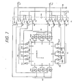
- Fig. 7 shows a partial configuration of a coordinate detecting apparatus according to the sixth embodiment.
- this embodiment comprises diode arrays 40, 41, 42 and 43, biasing means Vp and Vn, and bias switching means 44.
- Each of the diode arrays constitutes a second switching means.
- the diode array 40 comprises diodes D x1 , D X2 , D x3 ? D x4' D x5 and D xs
- the diode array 41 comprises diodes D x1 , , D x2', D x3 ', D x4 , , D x5 , and D x6 ,.
- the diodes D x1, D x2 , and D X3 are connected to the left end of the touch panel 22 through their cathodes, while their anodes are commonly connected to the terminal p2 of the bias switching means 44.
- the diodes D x4, D x5 and D x6 are connected to the cathodes of the diodes D x1, D x2 and D X3 through their anodes, respectively, while their cathodes are commonly connected to the terminal p1 of the bias switching means 44.
- the diode array 40 is associated with the left end of the touch panel 22.
- the diodes D x1' , D x2' and D X3 are connected to the right end of the touch panel 22 through their anodes while their cathodes are commonly connected to the terminal p5 of the bias switching means 44.
- the diodes D x4 , , D x5' and D x6' are connected to the anodes of the diodes Dx 1' , D x2, and D x3' through their cathodes, respectively, while their anodes are commonly connected to the terminal p6 of the bias switching means 44.
- the diode array 41 is associated with the right end of the touch panel 22.
- the diode array 42 comprises diodes Dy 1, Dy 2 , Dy 3 , D y4, D y5 and D y6, and the diode array 43 comprises diodes D y1 , , Dy 2 , , Dy 3 , , D Y4 , , D y5' and D y6' ,
- the diodes D y1, D Y2 and Dy 3 are connected to the top end of the touch panel 22 through their anodes, while their cathodes are commonly connected to the terminal p4 of the bias switching means 44.
- the diodes Dy 4 , D y5 and D y6 are connected to the anodes of the diodes D y1 , Dy 2 and D Y3 through their cathodes, respectively, while their anodes are commonly connected to the terminal p3 of the bias switching means 44.
- the diode array 42 is associated with the top end of the touch panel 22.
- the diodes D y1 , , D Y2 , and Dy 3 are connected to the bottom end of the touch panel 22 through their cathodes, while their anodes are commonly connected to the terminal p8 of the bias switching means 44.
- the diodes Dy 4 ,, Dy 5' and D y6 are connected to the cathodes of the diodes Dy1 , , Dy 2 , and D y3 , through their anodes, respectively, while their cathodes are commonly connected to the terminal p7 of the bias switching means 44.
- the diode array 43 is associated with the bottom end of the touch panel 22.
- each of the diode arrays in Fig. 7 comprises three serially connected pairs of diodes, the number of the diodes may be an appropriate different number.
- the terminals q1, r4, q5 and r7 are commonly connected to a positive voltage source Vp constituting the biasing means.
- the terminals r1, r2, q3 and q4 are connected to the common line L, shown in Fig. 6, and the terminals r5, r6, q7 and q8 are connected to the common line L 2 shown in Fig. 6.
- the terminals q2, r3, q6 and r8 are commonly connected to a negative voltage source Vn constituting the biasing means.
- the common lines L 1 and L 2 are alternately connected to the input and output of the op amp 15 in Fig. 6, respectively.
- the diodes in the diode arrays 40 and 41 are biased in reverse direction and substantially made be in open states, and only the diodes in the diodes arrays 42 and 43 associated with the ends in Y direction are biased in forward direction and made conductive.
- the data corresponding to the coordinate y of the point on the touch panel 22 can be acquired.
- the positive bias voltage Vp and negative bias voltage Vn should be set to have respective magnitudes larger than the peak voltage of the signal flowing through the load capacitance C B to the ground 17.
- Each of the serially connected diodes in each diode array may separately be connected to the corresponding end of the touch panel 22 as shown in Fig. 8. Although only the diode array 40 is illustrated in Fig. 8, the connections of the diodes D x1 , D x2 , D x3 , D x4 , D X5 and D X6 to the end of the touch panel 22 are separated from each other with a specified spacing d.
Landscapes
- Engineering & Computer Science (AREA)
- Theoretical Computer Science (AREA)
- General Engineering & Computer Science (AREA)
- Physics & Mathematics (AREA)
- General Physics & Mathematics (AREA)
- Human Computer Interaction (AREA)
- Artificial Intelligence (AREA)
- Computer Hardware Design (AREA)
- Computer Vision & Pattern Recognition (AREA)
- Position Input By Displaying (AREA)
- Measurement Of Length, Angles, Or The Like Using Electric Or Magnetic Means (AREA)
Claims (20)
Applications Claiming Priority (6)
| Application Number | Priority Date | Filing Date | Title |
|---|---|---|---|
| JP37914/84 | 1984-02-29 | ||
| JP37915/84 | 1984-02-29 | ||
| JP59037914A JPS60181913A (ja) | 1984-02-29 | 1984-02-29 | 座標検出装置 |
| JP37919/84 | 1984-02-29 | ||
| JP59037915A JPS60181914A (ja) | 1984-02-29 | 1984-02-29 | 座標検出装置 |
| JP59037919A JPS60181915A (ja) | 1984-02-29 | 1984-02-29 | 座標検出装置 |
Publications (2)
| Publication Number | Publication Date |
|---|---|
| EP0155781A1 EP0155781A1 (fr) | 1985-09-25 |
| EP0155781B1 true EP0155781B1 (fr) | 1988-10-19 |
Family
ID=27289642
Family Applications (1)
| Application Number | Title | Priority Date | Filing Date |
|---|---|---|---|
| EP85301314A Expired EP0155781B1 (fr) | 1984-02-29 | 1985-02-27 | Appareil détecteur de coordonnées |
Country Status (7)
| Country | Link |
|---|---|
| US (1) | US4680430A (fr) |
| EP (1) | EP0155781B1 (fr) |
| KR (1) | KR900002350B1 (fr) |
| AU (1) | AU552619B2 (fr) |
| CA (1) | CA1251537A (fr) |
| DE (1) | DE3565732D1 (fr) |
| ES (1) | ES8702007A1 (fr) |
Families Citing this family (68)
| Publication number | Priority date | Publication date | Assignee | Title |
|---|---|---|---|---|
| US4972496A (en) * | 1986-07-25 | 1990-11-20 | Grid Systems Corporation | Handwritten keyboardless entry computer system |
| US5157737A (en) * | 1986-07-25 | 1992-10-20 | Grid Systems Corporation | Handwritten keyboardless entry computer system |
| US6002799A (en) * | 1986-07-25 | 1999-12-14 | Ast Research, Inc. | Handwritten keyboardless entry computer system |
| US4806709A (en) * | 1987-05-26 | 1989-02-21 | Microtouch Systems, Inc. | Method of and apparatus for sensing the location, such as coordinates, of designated points on an electrically sensitive touch-screen surface |
| US4853498A (en) * | 1988-06-13 | 1989-08-01 | Tektronix, Inc. | Position measurement apparatus for capacitive touch panel system |
| US5305017A (en) * | 1989-08-16 | 1994-04-19 | Gerpheide George E | Methods and apparatus for data input |
| US5149918A (en) * | 1990-10-29 | 1992-09-22 | International Business Machines Corporation | Touch sensitive overlay |
| US5347295A (en) * | 1990-10-31 | 1994-09-13 | Go Corporation | Control of a computer through a position-sensed stylus |
| GB2266773A (en) * | 1992-05-07 | 1993-11-10 | Anthony David Raffe | Touch sensitive control |
| US5889236A (en) * | 1992-06-08 | 1999-03-30 | Synaptics Incorporated | Pressure sensitive scrollbar feature |
| US6028271A (en) * | 1992-06-08 | 2000-02-22 | Synaptics, Inc. | Object position detector with edge motion feature and gesture recognition |
| EP0574213B1 (fr) * | 1992-06-08 | 1999-03-24 | Synaptics, Inc. | Détecteur de position d'un objet |
| US5861583A (en) * | 1992-06-08 | 1999-01-19 | Synaptics, Incorporated | Object position detector |
| US5880411A (en) * | 1992-06-08 | 1999-03-09 | Synaptics, Incorporated | Object position detector with edge motion feature and gesture recognition |
| US6239389B1 (en) | 1992-06-08 | 2001-05-29 | Synaptics, Inc. | Object position detection system and method |
| US5451724A (en) * | 1992-08-05 | 1995-09-19 | Fujitsu Limited | Touch panel for detecting a coordinate of an arbitrary position where pressure is applied |
| US5554827A (en) * | 1993-02-22 | 1996-09-10 | Wacom Co., Ltd. | Method of and apparatus for determining whether a digitizer coordinate detecting tablet is properly operating and/or writing adjustment data into a memory associated with the tablet |
| US6476798B1 (en) | 1994-08-22 | 2002-11-05 | International Game Technology | Reduced noise touch screen apparatus and method |
| GB9422911D0 (en) * | 1994-11-14 | 1995-01-04 | Moonstone Technology Ltd | Capacitive touch detectors |
| US5757368A (en) * | 1995-03-27 | 1998-05-26 | Cirque Corporation | System and method for extending the drag function of a computer pointing device |
| JP3390292B2 (ja) * | 1995-07-25 | 2003-03-24 | アルプス電気株式会社 | 座標検出装置 |
| US6380929B1 (en) | 1996-09-20 | 2002-04-30 | Synaptics, Incorporated | Pen drawing computer input device |
| US5854625A (en) * | 1996-11-06 | 1998-12-29 | Synaptics, Incorporated | Force sensing touchpad |
| US5886687A (en) * | 1997-02-20 | 1999-03-23 | Gibson; William A. | Touch panel system utilizing capacitively-coupled electrodes |
| US6222528B1 (en) * | 1997-03-07 | 2001-04-24 | Cirque Corporation | Method and apparatus for data input |
| US6131047A (en) | 1997-12-30 | 2000-10-10 | Ericsson Inc. | Radiotelephones having contact-sensitive user interfaces and methods of operating same |
| US6262717B1 (en) | 1998-07-02 | 2001-07-17 | Cirque Corporation | Kiosk touch pad |
| JP3835972B2 (ja) * | 1999-06-02 | 2006-10-18 | シャープ株式会社 | 液晶表示装置 |
| US6730863B1 (en) | 1999-06-22 | 2004-05-04 | Cirque Corporation | Touchpad having increased noise rejection, decreased moisture sensitivity, and improved tracking |
| US6529122B1 (en) | 1999-12-10 | 2003-03-04 | Siemens Technology-To-Business Center, Llc | Tactile sensor apparatus and methods |
| TW494323B (en) * | 2000-08-29 | 2002-07-11 | Ibm | System and method for locating on a physical document items referenced in another physical document |
| TW528967B (en) | 2000-08-29 | 2003-04-21 | Ibm | System and method for locating on a physical document items referenced in an electronic document |
| US20030071798A1 (en) * | 2001-04-23 | 2003-04-17 | Ehud Baron | System and method for transmitting, receiving, and generating digital ink from triangulation data of a transponder-stylus |
| US6871395B2 (en) | 2001-08-06 | 2005-03-29 | Siemens Technology-To-Business Center, Llc. | Methods for manufacturing a tactile sensor using an electrically conductive elastomer |
| AU2002342797A1 (en) * | 2001-11-13 | 2003-05-26 | International Business Machines Corporation | System and method for selecting electronic documents from a physical document and for displaying said electronic documents over said physical document |
| US20030117378A1 (en) | 2001-12-21 | 2003-06-26 | International Business Machines Corporation | Device and system for retrieving and displaying handwritten annotations |
| US6888537B2 (en) | 2002-02-13 | 2005-05-03 | Siemens Technology-To-Business Center, Llc | Configurable industrial input devices that use electrically conductive elastomer |
| DE10212901A1 (de) * | 2002-03-23 | 2003-10-02 | Kostal Leopold Gmbh & Co Kg | Einrichtung zum Erfassen der Position eines beweglichen Elementes in einer zweidimensional ausgelegten Meßfeldanordnung |
| US6869239B2 (en) * | 2002-04-15 | 2005-03-22 | Charles Albert Morris | Compact keyboard with sliding motion key actuation |
| US6891531B2 (en) * | 2002-07-05 | 2005-05-10 | Sentelic Corporation | Sensing an object with a plurality of conductors |
| EP1550057A1 (fr) * | 2002-10-10 | 2005-07-06 | International Business Machines Corporation | Systeme et procede de selection, de commande et d'acces a une information protegee par les droits d'auteur a partir de documents physiques |
| US7310779B2 (en) * | 2003-06-26 | 2007-12-18 | International Business Machines Corporation | Method for creating and selecting active regions on physical documents |
| GB0319714D0 (en) | 2003-08-21 | 2003-09-24 | Philipp Harald | Anisotropic touch screen element |
| US7145552B2 (en) * | 2003-10-22 | 2006-12-05 | Solectron Corporation | Electric field proximity keyboards and detection systems |
| US20050110766A1 (en) * | 2003-11-24 | 2005-05-26 | Elo Touchsystems, Inc. | Touch sensor with conductive polymer switches |
| US20050110767A1 (en) * | 2003-11-24 | 2005-05-26 | Elo Touchsystems, Inc. | Method of manufacturing touch sensor with switch tape strips |
| US8050876B2 (en) * | 2005-07-18 | 2011-11-01 | Analog Devices, Inc. | Automatic environmental compensation of capacitance based proximity sensors |
| US7301351B2 (en) * | 2006-02-10 | 2007-11-27 | Milliken & Company | Printed capacitive sensor |
| US7208960B1 (en) * | 2006-02-10 | 2007-04-24 | Milliken & Company | Printed capacitive sensor |
| US7395717B2 (en) * | 2006-02-10 | 2008-07-08 | Milliken & Company | Flexible capacitive sensor |
| TWI308290B (en) * | 2006-03-17 | 2009-04-01 | Innolux Display Corp | Touch panel |
| US20070222764A1 (en) * | 2006-03-22 | 2007-09-27 | Centrality Communications, Inc. | Glide touch sensor based interface for navigation infotainment systems |
| US20070222767A1 (en) * | 2006-03-22 | 2007-09-27 | David Wang | Glide touch sensor based interface for navigation infotainment systems |
| US8121283B2 (en) | 2006-05-18 | 2012-02-21 | Cypress Semiconductor Corporation | Tapered capacitive sensing structure |
| US7876309B2 (en) | 2006-05-18 | 2011-01-25 | Cypress Semiconductor Corporation | Toothed slider |
| US8619054B2 (en) | 2006-05-31 | 2013-12-31 | Atmel Corporation | Two dimensional position sensor |
| US8040321B2 (en) * | 2006-07-10 | 2011-10-18 | Cypress Semiconductor Corporation | Touch-sensor with shared capacitive sensors |
| US8058937B2 (en) * | 2007-01-30 | 2011-11-15 | Cypress Semiconductor Corporation | Setting a discharge rate and a charge rate of a relaxation oscillator circuit |
| US8059103B2 (en) | 2007-11-21 | 2011-11-15 | 3M Innovative Properties Company | System and method for determining touch positions based on position-dependent electrical charges |
| US9007310B1 (en) * | 2008-02-29 | 2015-04-14 | Cypress Semiconductor Corporation | Single layer touch sensor with improved sensitivity and accuracy |
| WO2010059216A1 (fr) * | 2008-11-20 | 2010-05-27 | Cirque Corportion | Procédé et système pour mesurer la position sur un panneau tactile à capacité de surface à l’aide d’un condensateur volant |
| US8183875B2 (en) * | 2008-11-26 | 2012-05-22 | 3M Innovative Properties Company | System and method for determining touch positions based on passively-induced position-dependent electrical charges |
| US20100328241A1 (en) * | 2009-06-12 | 2010-12-30 | Keith Paulsen | Method and system for measuring position on surface capacitance touch panel using a flying capacitor |
| ES2370627B1 (es) * | 2010-01-14 | 2012-10-26 | Boix Maquinaria S.L. | Dispositivo transportador de planchas planas de cartón en máquinas formadoras de cajas de cartón. |
| US8692799B1 (en) | 2011-07-05 | 2014-04-08 | Cypress Semiconductor Corporation | Single layer multi-touch capacitive sensor |
| CN102799325B (zh) * | 2012-06-21 | 2016-03-30 | 敦泰科技有限公司 | 一种自电容触摸屏检测方法、装置和系统 |
| US20160378262A1 (en) * | 2012-06-21 | 2016-12-29 | Focaltech Electronics, Ltd. | Detection Method, Device And System For Detecting Self-Capacitance Touch Screen |
| EP3690913B1 (fr) * | 2017-09-29 | 2022-05-25 | Alps Alpine Co., Ltd. | Dispositif d'entrée d'actionnement et poignée de porte |
Family Cites Families (6)
| Publication number | Priority date | Publication date | Assignee | Title |
|---|---|---|---|---|
| US3449516A (en) * | 1965-12-27 | 1969-06-10 | Iit Res Inst | Graphical input system |
| US4103252A (en) * | 1976-11-26 | 1978-07-25 | Xerox Corporation | Capacitive touch-activated transducer system including a plurality of oscillators |
| DE3067729D1 (en) * | 1979-02-23 | 1984-06-14 | Peptek Inc | Touch panel system and method |
| US4476463A (en) * | 1981-08-24 | 1984-10-09 | Interaction Systems, Inc. | Display device having unpatterned touch detection |
| US4435616A (en) * | 1981-08-25 | 1984-03-06 | Kley Victor B | Graphical data entry apparatus |
| US4550310A (en) * | 1981-10-29 | 1985-10-29 | Fujitsu Limited | Touch sensing device |
-
1985
- 1985-02-14 AU AU38703/85A patent/AU552619B2/en not_active Ceased
- 1985-02-25 KR KR1019850001176A patent/KR900002350B1/ko not_active Expired
- 1985-02-27 EP EP85301314A patent/EP0155781B1/fr not_active Expired
- 1985-02-27 ES ES540763A patent/ES8702007A1/es not_active Expired
- 1985-02-27 CA CA000475287A patent/CA1251537A/fr not_active Expired
- 1985-02-27 DE DE8585301314T patent/DE3565732D1/de not_active Expired
- 1985-02-27 US US06/706,224 patent/US4680430A/en not_active Expired - Lifetime
Also Published As
| Publication number | Publication date |
|---|---|
| KR900002350B1 (ko) | 1990-04-12 |
| KR850006749A (ko) | 1985-10-16 |
| AU3870385A (en) | 1985-09-12 |
| EP0155781A1 (fr) | 1985-09-25 |
| ES540763A0 (es) | 1986-12-01 |
| DE3565732D1 (en) | 1988-11-24 |
| AU552619B2 (en) | 1986-06-12 |
| US4680430A (en) | 1987-07-14 |
| CA1251537A (fr) | 1989-03-21 |
| ES8702007A1 (es) | 1986-12-01 |
Similar Documents
| Publication | Publication Date | Title |
|---|---|---|
| US4680430A (en) | Coordinate detecting apparatus | |
| EP0229713B1 (fr) | Ecran tactile | |
| EP0492855A2 (fr) | Appareil de désignation de position | |
| US4678869A (en) | Position responsive apparatus, system and method having electrographic application | |
| US6081259A (en) | Method and apparatus for reducing noise in an electrostatic digitizer | |
| US5801682A (en) | Tactile designation device with high-resolution transparent capacitive surface | |
| US5790107A (en) | Touch sensing method and apparatus | |
| TWI433014B (zh) | 顯示裝置 | |
| EP0665508B1 (fr) | Dispositif de calcul portable commandé par mini-tablette sensitive | |
| US5847690A (en) | Integrated liquid crystal display and digitizer having a black matrix layer adapted for sensing screen touch location | |
| US10156949B2 (en) | Force-touch sensor with multilayered electrodes | |
| KR101447664B1 (ko) | 오버 드라이브 구동 방식의 터치 검출 장치 및 터치 검출 방법 | |
| US5920309A (en) | Touch sensing method and apparatus | |
| CA1200893A (fr) | Systeme d'electrographie | |
| JP2005140612A (ja) | 容量検出回路及び検出方法並びにそれを用いた指紋センサ | |
| WO1992010823A1 (fr) | Capteur et controleur a effleurement | |
| JPH05241717A (ja) | タッチパネル装置 | |
| JP2000047808A (ja) | 押圧検出兼用静電容量式座標検出装置 | |
| JP2003173238A (ja) | タッチセンサおよびタッチセンサ付き表示装置 | |
| US20070195069A1 (en) | Pen apparatus, system, and method of assembly | |
| JPS60181913A (ja) | 座標検出装置 | |
| JPH0118450B2 (fr) | ||
| JPS60181915A (ja) | 座標検出装置 | |
| KR20140011154A (ko) | 터치 검출 장치 및 터치 검출 방법 | |
| JPH05324164A (ja) | 位置検出装置 |
Legal Events
| Date | Code | Title | Description |
|---|---|---|---|
| PUAI | Public reference made under article 153(3) epc to a published international application that has entered the european phase |
Free format text: ORIGINAL CODE: 0009012 |
|
| AK | Designated contracting states |
Designated state(s): DE FR GB IT NL |
|
| 17P | Request for examination filed |
Effective date: 19851101 |
|
| 17Q | First examination report despatched |
Effective date: 19870616 |
|
| GRAA | (expected) grant |
Free format text: ORIGINAL CODE: 0009210 |
|
| AK | Designated contracting states |
Kind code of ref document: B1 Designated state(s): DE FR GB IT NL |
|
| REF | Corresponds to: |
Ref document number: 3565732 Country of ref document: DE Date of ref document: 19881124 |
|
| ET | Fr: translation filed | ||
| ITF | It: translation for a ep patent filed | ||
| PLBE | No opposition filed within time limit |
Free format text: ORIGINAL CODE: 0009261 |
|
| STAA | Information on the status of an ep patent application or granted ep patent |
Free format text: STATUS: NO OPPOSITION FILED WITHIN TIME LIMIT |
|
| 26N | No opposition filed | ||
| ITTA | It: last paid annual fee | ||
| PGFP | Annual fee paid to national office [announced via postgrant information from national office to epo] |
Ref country code: GB Payment date: 19921208 Year of fee payment: 9 |
|
| PGFP | Annual fee paid to national office [announced via postgrant information from national office to epo] |
Ref country code: FR Payment date: 19921229 Year of fee payment: 9 |
|
| PGFP | Annual fee paid to national office [announced via postgrant information from national office to epo] |
Ref country code: NL Payment date: 19930228 Year of fee payment: 9 |
|
| PG25 | Lapsed in a contracting state [announced via postgrant information from national office to epo] |
Ref country code: GB Effective date: 19940227 |
|
| PG25 | Lapsed in a contracting state [announced via postgrant information from national office to epo] |
Ref country code: NL Effective date: 19940901 |
|
| NLV4 | Nl: lapsed or anulled due to non-payment of the annual fee | ||
| GBPC | Gb: european patent ceased through non-payment of renewal fee |
Effective date: 19940227 |
|
| PG25 | Lapsed in a contracting state [announced via postgrant information from national office to epo] |
Ref country code: FR Effective date: 19941031 |
|
| REG | Reference to a national code |
Ref country code: FR Ref legal event code: ST |
|
| PGFP | Annual fee paid to national office [announced via postgrant information from national office to epo] |
Ref country code: DE Payment date: 20010221 Year of fee payment: 17 |
|
| PG25 | Lapsed in a contracting state [announced via postgrant information from national office to epo] |
Ref country code: DE Free format text: LAPSE BECAUSE OF NON-PAYMENT OF DUE FEES Effective date: 20020903 |