EP0156111A1 - Voltage réglé et puissance approximativement constante pour une tête d'impression thermique - Google Patents
Voltage réglé et puissance approximativement constante pour une tête d'impression thermique Download PDFInfo
- Publication number
- EP0156111A1 EP0156111A1 EP85100688A EP85100688A EP0156111A1 EP 0156111 A1 EP0156111 A1 EP 0156111A1 EP 85100688 A EP85100688 A EP 85100688A EP 85100688 A EP85100688 A EP 85100688A EP 0156111 A1 EP0156111 A1 EP 0156111A1
- Authority
- EP
- European Patent Office
- Prior art keywords
- electrodes
- current
- output
- input
- voltage
- Prior art date
- Legal status (The legal status is an assumption and is not a legal conclusion. Google has not performed a legal analysis and makes no representation as to the accuracy of the status listed.)
- Granted
Links
Images
Classifications
-
- B—PERFORMING OPERATIONS; TRANSPORTING
- B41—PRINTING; LINING MACHINES; TYPEWRITERS; STAMPS
- B41J—TYPEWRITERS; SELECTIVE PRINTING MECHANISMS, i.e. MECHANISMS PRINTING OTHERWISE THAN FROM A FORME; CORRECTION OF TYPOGRAPHICAL ERRORS
- B41J2/00—Typewriters or selective printing mechanisms characterised by the printing or marking process for which they are designed
- B41J2/315—Typewriters or selective printing mechanisms characterised by the printing or marking process for which they are designed characterised by selective application of heat to a heat sensitive printing or impression-transfer material
- B41J2/32—Typewriters or selective printing mechanisms characterised by the printing or marking process for which they are designed characterised by selective application of heat to a heat sensitive printing or impression-transfer material using thermal heads
- B41J2/35—Typewriters or selective printing mechanisms characterised by the printing or marking process for which they are designed characterised by selective application of heat to a heat sensitive printing or impression-transfer material using thermal heads providing current or voltage to the thermal head
- B41J2/355—Control circuits for heating-element selection
Definitions
- This invention relates to driver circuits for thermal printheads that generate localized heat in a ribbon in response to electrical current.
- the localized heat then serves to cause ink transfer from the ribbon to a receiving medium.
- the electrical signals are applied by printhead electrodes wiping across an outer layer of the ribbon which is characterized by moderate resistivity. These signals move inwardly to a layer that is highly conductive (typically an aluminum layer) with localized heating occurring in the process.
- the electrical circuit is completed by an electrode connected to ground which intersects the ribbon.
- EP-A-67.985 describes a voltage source regulated in response to a voltage sensed at the ribbon at a location spaced from the printing zone.
- This invention also employs a regulated voltage source.
- the voltage is regulated in response to the level sensed at each electrode through diodes connected to each electrode.
- EP-A-113.400 employs diodes connected to each electrode, but the signal is not used in a voltage-source system.
- This invention additionally employs a voltage-divider circuit to each electrode having a resistor between the regulated voltage output and the electrode, which resistor is selected to provide at nominal conditions the same voltage drop as that across the ribbon.
- EP-A-67.985 and US-A-4,420,758 disclosed as such resistcrs to limit current flow.
- This invention is a circuit to drive plural electrodes (typically forty) of a resistive ribbon printer.
- the voltage at each electrode is monitored, and the lowest voltage predominates as one control input to a differential amplifier.
- Monitoring is from a common node or point through diodes or other unidirectional devices, one connected in parallel with each electrode to pass high signals on the common point.
- the output of the differential amplifier drives all the electrodes, each in series with a substantially identical, separate resistor.
- the second input to the differential amplifier is at a set, reference-level difference from the output.
- the potential across the series resistor to the electrode with the lowest voltage is kept constant.
- the electrode with the lowest voltage thereby receives a fixed current, and the other electrodes are subject to limited power excursions.
- a similar, oppositely poled diode is connected between the common point of the monitoring diodes and the control input of the amplifier.
- the embodiment includes a constant-current source applied to all the diodes to maintain them in consistent operating ranges. The source need not be precise.
- Each of the separate resistors forms a voltage-divider circuit with the elements driven by the electrode it drives.
- the same power into the driven elements is approximated when the amplifier output is approximately twice the voltage across the driven elements and the voltage drop across the separate resistor is the same as the voltage drop across the driven elements at the nominal conditions.
- the level of amplifier output and the magnitude of the separate resistors are selected to provide this.
- this can be implemented by circuitry in which small voltage drop occurs across the switches to the electrodes. This permits the switches to be miniaturized and tightly packed on a standard ciicuit chip.
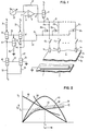
- Fig. 1 is a conventional schematic illustration of circuitry for printing by electrodes and Fig. 2 is an operating diagram illustrating the approximate constant power voltage-divider operation.
- electrodes la, 1b through 1n (a typical number of which is 40), have current driven through them to ground for printing.
- electrodes la through In are close together in a vertical column and in contact with a resistive ribbon 2, as is known and described, for example, in the documents discussed above under the heading "Background Art".
- Each electrode la through ln is solid metal having negligible resistance in this context of resistive ribbon printing.
- a ground connection which may be a roller 3, typically is firmly pressed against the ribbon 2 on the same side contacted by electrodes la through In.
- Ribbon 2 from the side is shown illustratively in exaggerated form in Fig. 1.
- Ribbon 2 is a lamination of constant cross-section.
- Layer 2a farthest from the electrodes, is the meltable ink.
- a thin internal layer 2b is a highly conductive layer, typically aluminum, which facilitates low-power conduction from areas directly across from electrodes la through In to ground roller 3.
- An aluminum layer 2b also inherently provides a thin, outer aluminum oxide surface which is relatively highly resistive.
- the resistive substrate 2c typically a carbon black filled polycarbonate resin, is contacted by electrodes la through In.
- Electrodes la through In are driven by operational amplifier 4, which functions as a differential amplifier as will be described.
- Amplifier 4 has a control input 5, which is the positive or plus input and a reference input 7, which is the negative or minus input.
- the plus and minus input designations are conventional, indicating that a rising signal on control input 5 is responsed tc by amplification providing a rising signal at the cutput 9 of amplifier 3. Conversely, a rising signal on reference input 7 is responsed to by amplification providing a falling signal at output 9.
- Amplifier 4 as a standard operational amplifier, provides reliable output with negligible input current on inputs 5 and 7. This facilitates overall circuit design and permits designs having a wide range of operability. It will be apparent, however, that amplifier systems having other characteristics can function for operational amplifier 4 so long as additional current flow and the like is compensated for or otherwise taken into account in each circuit design.
- Output 9 drives the base of bipolar transistor 11.
- the emitter of transistor 11 is connected to line 13, and the collector of transistor 13 is connected to operating voltage Vl, typically +38 volts.
- Transistor 11 thus serves to provide current isolation between output 9 and line 13, with a small voltage potential drop inserted by the inherent forward biased base-to-emitter drop of transistor 11. It will be recognized that transistor 11 is a simplified implementation of a power amplifier, for example, a Darlington pair of transistors.
- Line 13 is connected to all of the electrodes la through In by identical, individual resistors 15a, 15b through 15n, each connected in series circuit between line 13 and one electrode la, 1b through 1n, respectively. Also in series circuit between electrodes la, lb through 1n is a switch 17a, 17b through 17n, respectively.
- switches 17a through 17n are illustrated entirely symbolically as such switches for the purpose of selecting electrodes may be standard. In an actual embodiment, they each include individual transistors or, more preferably, a Darlington configuration of transistors, switched off-and-on by a signal to the base or the equivalent control input to thereby open and close the path through switches 17a through 17n.
- the voltage drop across a switched-on transistor switch 17a through 17n is negligible because the circuit is designed to operate the pertinent transistors in switches 17a through 17n in saturation).
- each electrode la through In and its associated resistor 15a through 15n, respectively, has one diode, 19a, 19b through 18n, respectively, connected to it.
- Diodes 19a through 19n are connected in a polarity to be non-conductive to or block signals provided by amplifier 9.
- the side of each diode 19a through 19n opposite the connection to the electrodes la through In connect to a common point 21.
- Diode 23, oppositely poled to diodes 19a through 19n, is connected in series between point 21 and control input 5, and as part of a current source as discussed below.
- Diode 23 and diodes 19a through 19n are selected to be virtually identical. They are mounted close together and in the same general environment and therefore have the same characteristics.
- diode 23 and only one of diodes 19a through 19n will be conducting during the great majority of printing operations. They will carry the same current and the voltage drop across the diode 23 and across the conducting one of diodes 19a through 19n will cancel, thereby providing on control input 5 a potential close to the lowest potential on electrodes la through In.
- V2 is the potential on line 13.
- Source 25 is an adjustable, constant-current source connected to reference input 7, which provides a current opposite in polarity and direction from that provided by V2.
- Source 25 is illustrated entirely symbolically, as such an adjustable current source is known as a control for electrode printing and forms no part of this invention.
- Resistor 27 is connected across input 7 to line 13.
- the system connected by line 29 to point 21 forms a source of constant current.
- the overall design approach to achieve constant current is considered conventional.
- Operating voltage V1 is connected through resistor 31 to the emitter of bipolar transistor 33.
- the base of transistor 33 is connected on line 35 to the base of transistor 37.
- Transistors 33 and 37 are selected to be virtually identical. They are mounted in generally the same environment and therefore have the same characteristics.
- the emitter of transistor 37 is connected to operating voltage Vl through resistor 39.
- Resistor 31 has twice the resistance of resistor 39 (typically resistor 31 is 2,000 ohms and resistor 39 is 1,000 ohms) to provide approximately twice the current out of the collector of transistor 37 than out of the collector of transistor 33, as is discussed further below.
- Line 43 carries the current out of the collector of transistor 33.
- Bipolar transistor 41 has its emitter connected to line 35 and its base connected to line 43. As the base-to-emitter path of transistor 41 has the base-to-collector of transistor 33 in parallel with it, current excursions from line 35 through transistor 41 are limited. Transistor 41 does provide a path to ground through resistor 45, connected from the collector of transistor 41 to ground, sufficient for current flow during normal operation. Line 43 also connects to the collector of bipolar transistor 49.
- the junction of the collector of transistor 37 and diode 23 is connected by line 29 to point 21.
- the opposite side of diode 23 is connected to line 47.
- Line 47 connects to the collector of transistor 51.
- Transistors 49 and 51 are selected to be virtually identical. They are mounted in generally the same environment and therefore have the same characteristics.
- the emitter of transistor 49 is connected through resistor 53 to V3, a source of operating voltage of opposite sense to voltage V1 (typically -5volts).
- the emitter of transistor 51 is connected to V3 through resistor 55.
- Resistors 53 and 55 have the same resistance (typically about 9000 ohms).
- the bases of transistors 49 and 51 are connected together on line 57 to ground.
- transistors 33 and 37 have bases at the same potential which are connected to V1 through resistances which are in a ratio of 1 to -. Accordingly, where current can flow normally through transistors 33 and 37, the current from the collector of transistcr 33 will be approximately one-half of that from the collector of transistor 37. (This ratio is approximate, rather than substantially exact, because the different currents will result in somewhat different operating characteristics).
- transistors 49 and 51 which have like characteristics, base-emitter junctions at the same potential, and emitters connected through identical resistors 53 and 55 to V3.
- Transistor 49 necessarily carries all the current from transistor 33 as line 43 is the only path for that current.
- Transistor 51 finds equilibrium only when it carries the same current, since a higher current would produce a drop across resistor 55 tending to lower the base-emitter vcltage.
- one or more of the switches 17a through 17n is closed. Selected ones of electrodes la through ln are connected to a diode 19a through 19n, respectively, when the intervening switch 17a through 17n is closed. That diode 19a through 19n connected to the electrode la through In of lowest potential is biased into conduction by the potential from line 29. All of the current on line 29 is carried by that one of diodes 19a through 19n. (Instances may occur where two or more switched-in ones of electrodes la through In are of such similarly low potential that more than one of diodes 19a through 19n conduct, but the frequency and duration are so limited as to be acceptable in normal printing. As will become clear below, the voltage seen at control input 5 will be slightly, but not drastically affected).
- reference current source 25 is set at a level defining a level of current to electrodes la through In defining a desired extent of printing. (In resistive ribbon printing, increased current normally increases heat created in the ribbon and darkens printing).
- V7 is on the minus input of amplifier 9. Where it is lower than the potential at the control input V5, the voltage at output 9 increases immediately by action of amplifier 4. Where V7 is higher than V5, the signal on output 9 immediately falls.
- Electrodes la through In having higher potential are driven by the same potential, V2, acting through an identical one of resistors 15a through 15n.
- the current to such higher-voltage electrodes is limited in proportion to the higher voltage, thereby preventing power excursions which typically damage the ribbon or other material which receives current from the electrodes la through In.
- Such higher voltage may be a resuJt of poor contact between an electrode la through In with a surface to which it connects.
- V2 and resistors 15a through 15n which are of identical resistivity, are selected to be within desired operating characteristics of the ribbon 2 or other medium driven by electrodes la through In.
- the magnitude of V2 and resistors 15a through 15n is selected more specifically to achieve approximately constant power delivered into the ribbon 2. Delivery of constant power produces more uniform printing operation and limits current flow. Current fluctuations are reduced, which reduces arcing tendencies.
- Constant power is approximated by selecting each resistor 15a through 15n equal to the nominal effective resistance into each of the electrodes la through In. (The nominal effective resistance is, of course, identical for all the electrodes la through In).
- Fig. 2 is a plot of the typical characteristic curve 60 of a ribbon 2 for voltage directly across the ribbon, Va, and current through one electrode, Iel. Normally, for predictable operation, the fast rising knee at the left of the characteristic curve is avoided and a nominal operation point is selected past the knee, such as a point 62. This nominal operating point has a voltage into the ribbon of Vn and a current In, resulting in power of Vn ⁇ In.
- Va The voltage directly across the ribbon, Va, is often termed the through voltage.
- the ribbon has an internal metal or other highly conductive layer 2b, thereby facilitating conduction along the ribbon to ground roller 3 and keeping Vc low.
- Va produces the heating effect for printing and is therefore the voltage which interacts with Iel to determine the degree of printing.
- Vc varies significantly with the number of electrodes la through 1n driven.
- Diodes 19a through 19n sense the combined voltage of Va and Vc. Since the regulated system is designed to provide a constant current to the electrode la through In having the lowest voltage, changes in Vc are neutralized. A change in Vc appears in the same sense at the diodes 19a through 19n, and the output of amplifier 4 responds to the changed input on control input 5 to change the output voltage on line 13 to maintain the constant current, thereby counteracting the change in Vc.
- any operating point must be found on a straight line 66 having a slope defined by the resistivity of one resistor 15a through 15n, which resistivity may be denominated R15.
- a straight line will closely follow the curved line when it is tangent to it.
- the tangent is found as follows.
- nominal operation is described as follows :
Landscapes
- Electronic Switches (AREA)
Applications Claiming Priority (2)
| Application Number | Priority Date | Filing Date | Title |
|---|---|---|---|
| US593052 | 1984-03-26 | ||
| US06/593,052 US4531134A (en) | 1984-03-26 | 1984-03-26 | Regulated voltage and approximate constant power for thermal printhead |
Publications (2)
| Publication Number | Publication Date |
|---|---|
| EP0156111A1 true EP0156111A1 (fr) | 1985-10-02 |
| EP0156111B1 EP0156111B1 (fr) | 1988-09-14 |
Family
ID=24373164
Family Applications (1)
| Application Number | Title | Priority Date | Filing Date |
|---|---|---|---|
| EP85100688A Expired EP0156111B1 (fr) | 1984-03-26 | 1985-01-24 | Voltage réglé et puissance approximativement constante pour une tête d'impression thermique |
Country Status (5)
| Country | Link |
|---|---|
| US (1) | US4531134A (fr) |
| EP (1) | EP0156111B1 (fr) |
| JP (1) | JPS60201970A (fr) |
| CA (1) | CA1223149A (fr) |
| DE (1) | DE3564918D1 (fr) |
Families Citing this family (8)
| Publication number | Priority date | Publication date | Assignee | Title |
|---|---|---|---|---|
| US4575731A (en) * | 1984-10-30 | 1986-03-11 | International Business Machines Corporation | Electro resistive printhead drive level sensing and control |
| US5053790A (en) * | 1990-07-02 | 1991-10-01 | Eastman Kodak Company | Parasitic resistance compensation for thermal printers |
| US5132709A (en) * | 1991-08-26 | 1992-07-21 | Zebra Technologies Corporation | Apparatus and method for closed-loop, thermal control of printing head |
| JPH05270036A (ja) * | 1992-03-27 | 1993-10-19 | Rohm Co Ltd | サーマルプリントヘッド |
| EP0568162A1 (fr) * | 1992-04-29 | 1993-11-03 | Francotyp-Postalia GmbH | Dispositif pour la commande d'une tête d'impression électrothermique |
| DE4214545C2 (de) * | 1992-04-29 | 1996-08-14 | Francotyp Postalia Gmbh | Anordnung für eine ETR-Druckkopfansteuerung |
| DE4221275C2 (de) * | 1992-06-26 | 1994-04-21 | Francotyp Postalia Gmbh | Ansteuerschaltung für eine elektrothermische Druckvorrichtung mit Widerstandsband |
| US5623297A (en) * | 1993-07-07 | 1997-04-22 | Intermec Corporation | Method and apparatus for controlling a thermal printhead |
Citations (4)
| Publication number | Priority date | Publication date | Assignee | Title |
|---|---|---|---|---|
| US4330786A (en) * | 1979-06-18 | 1982-05-18 | Mitsubishi Denki Kabushiki Kaisha | Method of controlling thermally controlling a thermal printing head |
| DE3202185A1 (de) * | 1981-02-03 | 1982-08-12 | Canon K.K., Tokyo | "thermodrucker" |
| EP0067969A2 (fr) * | 1981-06-19 | 1982-12-29 | International Business Machines Corporation | Circuit de commande pour imprimante thermique |
| US4434356A (en) * | 1982-12-22 | 1984-02-28 | International Business Machines Corporation | Regulated current source for thermal printhead |
Family Cites Families (4)
| Publication number | Priority date | Publication date | Assignee | Title |
|---|---|---|---|---|
| JPS5353223A (en) * | 1976-10-25 | 1978-05-15 | Epson Corp | Circuit for compensating voltage of thermal printer |
| JPS57110466A (en) * | 1980-12-29 | 1982-07-09 | Ricoh Co Ltd | Thermosentivie recorder |
| GB2099763B (en) * | 1981-05-26 | 1985-12-04 | Ricoh Kk | Electrothermal non-impact recording method |
| US4384797A (en) * | 1981-08-13 | 1983-05-24 | International Business Machines Corporation | Single laminated element for thermal printing and lift-off correction, control therefor, and process |
-
1984
- 1984-03-26 US US06/593,052 patent/US4531134A/en not_active Expired - Fee Related
- 1984-12-14 JP JP59263159A patent/JPS60201970A/ja active Granted
-
1985
- 1985-01-24 DE DE8585100688T patent/DE3564918D1/de not_active Expired
- 1985-01-24 EP EP85100688A patent/EP0156111B1/fr not_active Expired
- 1985-02-06 CA CA000473700A patent/CA1223149A/fr not_active Expired
Patent Citations (4)
| Publication number | Priority date | Publication date | Assignee | Title |
|---|---|---|---|---|
| US4330786A (en) * | 1979-06-18 | 1982-05-18 | Mitsubishi Denki Kabushiki Kaisha | Method of controlling thermally controlling a thermal printing head |
| DE3202185A1 (de) * | 1981-02-03 | 1982-08-12 | Canon K.K., Tokyo | "thermodrucker" |
| EP0067969A2 (fr) * | 1981-06-19 | 1982-12-29 | International Business Machines Corporation | Circuit de commande pour imprimante thermique |
| US4434356A (en) * | 1982-12-22 | 1984-02-28 | International Business Machines Corporation | Regulated current source for thermal printhead |
Also Published As
| Publication number | Publication date |
|---|---|
| JPH051147B2 (fr) | 1993-01-07 |
| DE3564918D1 (en) | 1988-10-20 |
| CA1223149A (fr) | 1987-06-23 |
| JPS60201970A (ja) | 1985-10-12 |
| EP0156111B1 (fr) | 1988-09-14 |
| US4531134A (en) | 1985-07-23 |
Similar Documents
| Publication | Publication Date | Title |
|---|---|---|
| EP0067969B1 (fr) | Circuit de commande pour imprimante thermique | |
| US4396923A (en) | Recording control apparatus | |
| US4350449A (en) | Resistive ribbon printing apparatus and method | |
| US4250512A (en) | Heating device for recording heads in ink mosaic recorders | |
| US6068360A (en) | Printer head drive system having negative feedback control | |
| EP0156111B1 (fr) | Voltage réglé et puissance approximativement constante pour une tête d'impression thermique | |
| EP0113400B1 (fr) | Source de courant ajustée pour tête d'impression thermique | |
| US5163760A (en) | Method and apparatus for driving a thermal head to reduce parasitic resistance effects | |
| US4564749A (en) | Heater drive circuit for controlling ink temperature in ink jet printer | |
| US5329304A (en) | Remaining ink detecting device and ink jet head cartridge | |
| JPH071731A (ja) | 熱式インク・ジェット・プリンタにおける発熱抵抗器への電力制御回路 | |
| US4701635A (en) | Current driving circuit with CMOS inverter | |
| US4176272A (en) | MOS-bipolar printer driver circuit | |
| EP0180049B1 (fr) | Dispositif de commande à réglage de la tension pour tête d'impression avec détection sur la tête d'impression | |
| US4542281A (en) | Thermal printer contrast control | |
| US2377783A (en) | Record sensing means | |
| EP0442391B1 (fr) | Circuit destiné à la protection contre surtension à l'entrée d'un circuit intégré alimenté par une source de tension | |
| EP0370765A2 (fr) | Cartouche pour tête d'impression à jet d'encre avec détecteur d'encre résiduelle | |
| EP0113817B1 (fr) | Compensation des marges dans les imprimantes thermiques | |
| EP0481277B1 (fr) | Source de courant | |
| JPH06201486A (ja) | 温度検出装置 | |
| US20020070989A1 (en) | Circuit for driving heater of printhead and device employing the same | |
| JPH0552792B2 (fr) | ||
| JPH01114919A (ja) | 電圧調整装置 | |
| JPS5820473A (ja) | サ−マルプリンタの印字方法 |
Legal Events
| Date | Code | Title | Description |
|---|---|---|---|
| PUAI | Public reference made under article 153(3) epc to a published international application that has entered the european phase |
Free format text: ORIGINAL CODE: 0009012 |
|
| AK | Designated contracting states |
Designated state(s): DE FR GB |
|
| 17P | Request for examination filed |
Effective date: 19860124 |
|
| 17Q | First examination report despatched |
Effective date: 19870206 |
|
| GRAA | (expected) grant |
Free format text: ORIGINAL CODE: 0009210 |
|
| AK | Designated contracting states |
Kind code of ref document: B1 Designated state(s): DE FR GB |
|
| REF | Corresponds to: |
Ref document number: 3564918 Country of ref document: DE Date of ref document: 19881020 |
|
| ET | Fr: translation filed | ||
| PLBE | No opposition filed within time limit |
Free format text: ORIGINAL CODE: 0009261 |
|
| STAA | Information on the status of an ep patent application or granted ep patent |
Free format text: STATUS: NO OPPOSITION FILED WITHIN TIME LIMIT |
|
| 26N | No opposition filed | ||
| REG | Reference to a national code |
Ref country code: FR Ref legal event code: GC |
|
| REG | Reference to a national code |
Ref country code: GB Ref legal event code: 732 |
|
| REG | Reference to a national code |
Ref country code: FR Ref legal event code: TP |
|
| PGFP | Annual fee paid to national office [announced via postgrant information from national office to epo] |
Ref country code: FR Payment date: 19951213 Year of fee payment: 12 |
|
| PGFP | Annual fee paid to national office [announced via postgrant information from national office to epo] |
Ref country code: GB Payment date: 19951228 Year of fee payment: 12 Ref country code: DE Payment date: 19951228 Year of fee payment: 12 |
|
| PG25 | Lapsed in a contracting state [announced via postgrant information from national office to epo] |
Ref country code: GB Effective date: 19970124 |
|
| GBPC | Gb: european patent ceased through non-payment of renewal fee |
Effective date: 19970124 |
|
| PG25 | Lapsed in a contracting state [announced via postgrant information from national office to epo] |
Ref country code: FR Effective date: 19970930 |
|
| PG25 | Lapsed in a contracting state [announced via postgrant information from national office to epo] |
Ref country code: DE Effective date: 19971001 |
|
| REG | Reference to a national code |
Ref country code: FR Ref legal event code: ST |