EP0157306A2 - Unité de traitement ultra-rapide - Google Patents
Unité de traitement ultra-rapide Download PDFInfo
- Publication number
- EP0157306A2 EP0157306A2 EP85103348A EP85103348A EP0157306A2 EP 0157306 A2 EP0157306 A2 EP 0157306A2 EP 85103348 A EP85103348 A EP 85103348A EP 85103348 A EP85103348 A EP 85103348A EP 0157306 A2 EP0157306 A2 EP 0157306A2
- Authority
- EP
- European Patent Office
- Prior art keywords
- instruction
- instructions
- high speed
- speed processor
- control means
- Prior art date
- Legal status (The legal status is an assumption and is not a legal conclusion. Google has not performed a legal analysis and makes no representation as to the accuracy of the status listed.)
- Granted
Links
Images


Classifications
-
- G—PHYSICS
- G06—COMPUTING OR CALCULATING; COUNTING
- G06F—ELECTRIC DIGITAL DATA PROCESSING
- G06F9/00—Arrangements for program control, e.g. control units
- G06F9/06—Arrangements for program control, e.g. control units using stored programs, i.e. using an internal store of processing equipment to receive or retain programs
- G06F9/30—Arrangements for executing machine instructions, e.g. instruction decode
- G06F9/38—Concurrent instruction execution, e.g. pipeline or look ahead
- G06F9/3877—Concurrent instruction execution, e.g. pipeline or look ahead using a secondary processor, e.g. coprocessor
Definitions
- the present invention pertains to a high speed processor in a computer system for assisting a main processor in the execution of instructions by executing certain selected instructions forming a subset of the instructions, the selected instructions being simple and more frequently executed by the computer system.
- each of at least two processors execute all of the instructions of one program, and operate simultaneously or concurrently for the purpose of improving the reliability of the processor portion of the computer system; and (2) in the second type, each of at least two processors execute different programs or perform different tasks or functions.
- the performance of a computer system is based, in part, upon the speed at which the processor or processors within the computer system execute a set of instructions.
- the set of instructions are executed sequentially, each of the instructions being executed at a certain rate.
- Some of the instructions which comprise the set of instructions are easy to implement in hardware and may be classified as simple instructions.
- Other instructions are more difficult to implement in hardware and may be classified as complex instructions.
- the simple instructions are more frequently executed than are the complex instructions.
- the instructions of the set of instructions (including the simple, more frequently executed instructions) are usually executed sequentially at the certain rate.
- the performance of the computer system may be measured in terms of the time elapsed in sequentially executing each of the instructions of the set of instructions, the performance of the computer system could be improved if the simple, more frequently executed instructions within the set of instructions are executed more rapidly than the complex, less frequently executed instructions.
- the multiprocessor system of the present invention is classified within a third type of multiprocessor system as contrasted with the first type and the second type of multiprocessor system discussed in the description of the prior art section of this application.
- the third type one program is executed by both of the processors of the multiprocessor system; however, each processor executes a different subset of instructions of the one program.
- the processors execute their instructions of the one program non-concurrently, that is, when one processor is executing an instruction, the operation of the other processor is suspended.
- One processor executes selected, specific instructions of the one program for the purpose of improving the performance of the computer system.
- the selected, specific instructions of the one program, executed by the one processor are "simple" and “more frequently executed” than are the other "complex" instructions of the one program.
- the one processor is also designed to execute the selected instructions very rapidly for the purpose of improving the performance of the computer system. This particular processor is termed a "high speed processor”.
- the rapid execution of the selected "simple" and "more frequently executed” instructions is accomplished by overlapping the execution of two sequential instructions. That is, while a simple instruction is being executed, the next instruction in the sequence is being prepared for execution.
- the high speed processor is not executing a simple instruction
- the other processor the main processor of the computer system, is executing the complex, less frequently executed instructions. Therefore, the instruction processing time, associated with the execution of the set of instructions of the one program, is decreased by a factor of approximately 40 %.
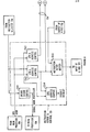
- a conventional data processing system 10 including a memory 10a, a main processor 10b connected to the memory 10a via lines 10e, 10f, and 10g and a control storage 10c representing a Read Only Memory (ROM) connected to the main processor 10b.
- the memory 10a includes a main storage 10a1 and a cache subsystem 10a2 connected to the main storage 10a1.
- Line 10e interconnects the cache subsystem 10a2 to the main processor 10b and is utilized for the transfer of data.
- Lines lOf/lOg are utilized for the transfer of instructions.
- the main processor 10b is connected to various peripheral devices via an input/output line 10d.
- a high speed processor 12 is interconnected between memory 10a and main processor 10b via lines 10f and 10g.
- the high speed processor 12 receives instructions from memory 10a. Of those instructions received by the high speed processor 12, some instructions are more frequently executed than others.
- the high speed processor 12 determines if a received instruction falls within the "more frequently executed" category. If the received instruction does fall within this category, the main processor 10b is prevented from executing the instruction, and the high speed processor 12 executes the instruction. However, if the instruction does not fall within the "more frequently executed” category, the high speed processor 12 signals the main processor 10b. As a result, the main processor 10b is permitted to execute the instruction. In this case, the operation of the high speed processor 12 is suspended.
- the high speed processor 12 is specifically designed to execute certain selected instructions which fall within the "more frequently executed” category, the speed at which these selected instructions are executed by the high speed processor 12 is much greater than the speed at which the other remaining instructions are executed by the main processor. Therefore, the performance of the computer system of the present invention, utilizing the high speed processor, is optimized and/or increased relative to the computer system of the prior art, wherein the high speed processor 12 is not utilized.
- the high speed processor 12 comprises an instruction buffer 12a connected to memory 10a for temporarily storing an instruction to be executed.
- An instruction register 12b is connected to the instruction buffer 12a for receiving the instruction and executing the instruction.
- An output of the instruction register 12b is connected to the main processor 10b for transferring the instruction to the main processor 10b.
- the main processor 10b will execute the instruction in the event the instruction cannot be executed by the high speed processor 12.
- the output of the instruction register 12b is also connected to an instruction decode and control circuit 12c for decoding the instruction being executed in the instruction register 12b.
- the main processor 10b is connected to the instruction decode and control circuit 12c for supplying address information associated with locations within the general purpose registers 12d in the event the main processor desires to retrieve one or more operands from the general purpose registers 12d for the purpose of executing the current instruction.
- the instruction decode and control unit 12c is connected to the main processor 10b via a line labelled "signal main processor" for the purpose of signalling the main processor to either execute the instruction or not execute the instruction. If the "signal main processor" line is high (binary 1), the main processor 10b will execute the instruction. However, if the "signal main processor” line is low (binary 0), the main processor will be prevented from executing the instruction. If the main processor 10b fails to execute the instruction, the high speed processor 12 will execute the instruction.
- the instruction decode and control circuit 12c is connected to a set of general purpose registers 12d via line 12e.
- the general purpose registers 12d are connected to an arithmetic logic unit (ALU) 12f via an A-register 12g.
- the general purpose registers 12d are also connected to the ALU 12f via a B-register 12h.
- An output of the A-register 12g is connected to an input of the instruction decode and control circuit 12ce
- the output of the A-register 12g is also connected to an input of the main processor 10b for transferring the data (such as operands) stored in the general purpose registers 12d to the main processor 10b in the event the main processor is executing the instruction.
- the output of the instruction register 12b is also connected to a displacement register 12S for storing a displacement value therein.
- the output of the displacement register 12S is connected to the ALU 12f via line 12M.
- An output of the ALU 12f is connected to an input of a D-register 12i.
- An output of the instruction decode and control circuit 12c is further connected to the input of the D-register 12i.
- An output of the D-register 12i is connected to an input of the A-register 12g, the B-register 12h, and the general purpose registers 12d.
- An output of the D-register 12i is also connected to an input of the memory 10a.
- the memory 10a is connected to an input of a data register 12j.
- An output of the D-register 12i is also connected to another input of the data register 12j.
- An output of the general purpose registers 12d which is connected to the A-register 12 g , is connected to another input of the data register 12j via line 12Q.
- An output of the general purpose registers 12d which is connected to the B-register 12h, is connected to another input of the data register 12j via line 12R.
- An output of the data register 12j is connected to a byte shifter 12k for shifting the incoming bytes of data a certain amount in order to properly align the first bit of the data byte with a correct first bit position for the byte of data.
- the byte shifter 12k is connected to an input of the B-register 12h.
- the byte shifter 12k is also connected to an input of an OR gate 12L and to memory 10a.
- the output of the - general purpose registers 12d, which is connected to the A-register 12g, is also connected to another input of the OR gate 12L.
- An output of OR gate 12L is connected to another input of the instruction register 12b.
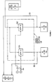
- the instruction decode and control circuit 12c comprises an opcode decode control circuit 12cl connected to the instruction register 12b for decoding the opcode of the instruction residing in the instruction register 12b to determine the type of instruction, for example, an EXECUTE instruction.
- the output of the opcode decode and control circuit 12cl is connected to the main processor 10b. If.the opcode decode control circuit 12cl determines, from the instruction opcode, that the instruction falls within the "more frequently executed" type, the output signal generated from the opcode decode and control circuit 12cl, labelled "signal main processor", will be low (i.e.
- the main processor 10b In response to this low output signal, the main processor 10b will not execute the instruction. However, the high speed processor 12 will execute the instruction. If the opcode decode control circuit 12cl determines that the instruction does not fall within the "more frequently executed" type, the output signal generated from the opcode decode and control circuit 12c1 will be high (a binary 1). In response to this high output signal, the main processor 10b will execute the instruction and the high speed processor suspends its operation.
- the instruction decode and control circuit 12c further comprises a GPR A address control 12c2 and a GPR a address control 12c3 connected to the instruction register 12b for receiving and storing the address information from the instruction stored in the instruction register 12b.
- An output from the GPR A address control 12c2 and an output from the GPR B address control 12c3 collectively constitute line 12e, line 12e being connected to the general purpose registers 12d.
- the instruction register 12b is also connected to a GPR address compare circuit 12c4.
- An output of the GPR A address control circuit 12c2 is also connected to the GPR address compare circuit 12c4.
- the GPR address compare circuit 12c4 compares the incoming address, destined for storage in the GPR A address control 12c2, with the address being generated from the GPR A address control circuit 12c2, and suspends the execution of the next instruction if the compared addresses are the same.
- the address compare circuit 12c4 may wrap the result from ALU 12f back into the B-register 12h in order to allow further processing on said result.
- the GPR address compare circuit 12c4 In view of the overlapped execution of two sequential instructions mentioned previously, if the incoming address from the next instruction to be executed is the same as the address being generated from the GPR A address control circuit 12c2, associated with the current instruction being executed, the GPR address compare circuit 12c4 generates a disable overlap signal.
- the disable overlap signal (1) prevents the instruction decode and control circuit 12c from addressing the general purpose registers 12d via line 12e, (2) prevents the A-register 12g-and the B-register 12h from being enabled, and (3) prevents the next instruction from being pre-decoded by the opcode decode control circuit 12c1.
- the disable overlap signal generated from the address compare circuit 12c4 will prevent the operands associated with next instruction from being withdrawn from the general purpose registers 12d.
- the output of the GPR A address control circuit 12c2 is also connected to one input of an instruction retry buffer 12c5.
- the output from the A-register 12g is connected to another input of the instruction retry buffer 12c5.
- An output from the instruction retry buffer 12c5 is connected to the input of the D-register 12i.
- the general purpose registers 12d comprise a general purpose A group of registers 12dl (GPR A) and a general purpose B group of registers 12d2 (GPR B).
- GPR A general purpose A group of registers 12dl
- GPR B general purpose B group of registers 12d2
- the output from the D-register 12i is connected to each of the GPR A group and the GPR B group, 12d1 and 12d2, respectively.
- the GPR A address control 12c2 is connected to the GPR A group 12d1 via line 12e.
- the GPR B address control 12c3 is connected to the GPR B group 12d2 via line 12e.
- the GPR A address control 12c2 and the GPR B address control 12c3 are address registers fro addressing locations within the GPR A group 12dl and the GPR B group 12d2, respectively.
- the GPR A group 12dl is connected to the input of A-register 12g.
- the GPR B group 12d2 is connected to the input of B-register 12h.
- Each of the outputs from GPR A group and GPR B group are connected to the input of the data register 12j.
- a chart 20 is illustrated, the chart. including several example “simple” and “more frequently executed” instructions and including several example “complex” and “less frequently executed” instructions.
- the chart is subdivided into three columns.
- a first column 20a includes a plurality of instruction acronyms.
- a second column 20b includes a plurality of instruction opcodes, an opcode corresponding to each instruction acronym of column 20a.
- a third column 20c includes a plurality of percent mix figures, a mix figure corresponding to each instruction acronym of column 20a.
- An instruction acronym identifies a particular instruction. Since each instruction possesses a specific opcode, an instruction opcode also identifies a particular instruction.
- the first and second columns 20a and 20b of chart 20 include instruction acronyms and opcodes for identifying specific instructions. Each instruction, on the average, appears in a set of instructions a certain plurality of times. When a figure representing the certain plurality is divided by the total number of instructions in the set of instructions, a percent mix figure is the result. Therefore, the third column 20c of chart 20 includes a plurality of mix figures, each mix figure representing a percentage of the total number of instructions within the set of instructions.
- instructions “BC”, “L”, and “ST” represent approximately 19 %, 13 %, and 6 % of the total number of instructions within a set of instructions.
- instructions “XC”, “MVCL”, and “MVC” represent approximately 0.5 %, 0.06 %, and 1.5 % of the total number of instructions within the set of instructions. Based on these percentage mix figures, instructions “BC”, “L”, and “ST” represent simple, more frequently executed instructions whereas instructions “XC”, “MVCL”, and “MVC” represent complex, less frequently executed instructions.
- the opcode decode control circuit 12cl includes a NOR gate 12c1(a).
- the input terminals of the NOR gate 12cl(a) are connected to the instruction register 12b via a plurality of opcode decoders 12cl(c).
- An opcode decoder 12cl(c) is connected to each of the input terminals of the NOR gate 12cl(a).
- Each of the opcode decoders 12c1(c) are designed to decode and respond to a different instruction opcode.
- the opcode of the instruction is "47". Therefore, as shown in Figure 6, the first opcode decoder 12c1(c), connected to the first input terminal of the NOR gate 12c1(a), is designed to decode and respond to this instruction, the first opcode decoder generating an output signal. However, the other opcode decoders 12c1(c) fail to decode and respond to this opcode, since they are designed to decode and respond to different instruction opcodes.
- the output terminal of the NOR gate 12c1(a) is connected to the main processor 10b and generates the "signal main processor" output signal as shown in Figures 2 and 3.
- the NOR gate 12c1(a) comprises an OR gate 12cl (a) (1) and an inverter 12cl(a)(2) connected to the output of the OR gate 12cl(a)(1).
- An instruction is withdrawn from memory 10a and is received by the high speed processor 12. If the instruction is one of a set of "more frequently executed” instructions, the high speed processor 12 executes the instruction. The main processor 10b is prevented from executing the instruction. However, if the instruction is not one of the set of "more frequently executed” instructions, the main processor 10b is not prevented from executing the instruction. In this case, the main processor 10b executes the instruction and the high speed processor 12 suspends its operation until the main processor 10b completes execution of the instruction.
- the control storage 10c is a Read Only Memory containing certain specific microcode instructions stored therein which are utilized to assist the main processor in the execution of an instruction.
- the main processor 10b executes the instruction in accordance with the microcode instructions stored within the control storage 10c. Since a large proportion of the instructions withdrawn from memory 10a fall within the "more frequently executed" category, these instructions are executed by the high speed processor 12.
- the high speed processor 12 executes the instructions, it is operating in an overlap execution mode.
- the high speed processor 12 is executing a first instruction, it is preparing to commence execution of a second instruction in a sequence of instructions.
- the high speed processor 12 is capable of executing the "more frequently executed” instructions more rapidly than would be possible if the main processor 10b were to execute the selected "more frequently executed” instructions.
- the instruction processing time, associated with the execution of the instructions withdrawn from memory 10a, is decreased by a factor of approximately forty percent (40 %). Therefore, the performance of the computer system of the present invention is improved relative to the computer systems of the prior art.
- An instruction is withdrawn from memory 10a and is received by the high speed processor 12.
- the instruction is temporarily stored in the instruction buffer 12a and is considered the "next instruction to be executed”.
- the instruction is subsequently transmitted to and stored in the instruction register 12b for execution.
- the opcode decode and control circuit 12cl of the instruction decode and control circuit 12c decodes the instruction for the purpose of determining if said instruction falls within the "more frequently executed” category. If the instruction does not fall within this category, the opcode decode control circuit 12c1 generates a high output signal, this high output signal being the "signal main processor" signal. In response to this high output signal, the main processor 10b executes the instruction.
- the operation of the high speed processor 12 is suspended.
- the opcode decode and control circuit 12cl determines that the instruction does fall within the "more frequently executed” category, the "signal main processor" output signal from the opcode decode control circuit 12cl remains low. Therefore, the main processor 10b is prevented from executing this instruction.
- the instruction address information associated with a first operand and further instruction address information associated with a second operand is stored in the GPR A address control 12c2 and the GPR B address control 12c3, respectively.
- the instruction stored in the instruction register 12b is an ADD instruction and that two operands are to be added together, the sum of the two operands being stored in the general purpose registers 12d.
- both operands are currently stored in the general purpose registers 12d, one operand being stored in the GPR A group 12d1 and the other operand being stored in the GPR B group 12d2.
- the contents of the GPR A group 12dl is an exact copy of the contents of the GPR B group 12d2.
- the address-information stored in the GPR A address control 12c2 is used to address the GPR A group 12dl, and the address information stored in the GPR B address control 12c3 is used to address the GPR B group 12d2.
- groups 12d1 and 12d2 are simultaneously addressed by the address controls 12c2 and 12c3, respectively.
- the operands stored therein are simultaneously withdrawn and stored in the A-register 12g and the B-register 12h, respectively.
- the arithmetic logic unit (ALU) 12f retrieves the operands from the A-register and the B-register and performs the instruction operation on the two operands, that is, adds them together forming a sum of the two operands.
- the sum is stored in the GPR A group 12dl and in the GPR B group 12d2 within the general purpose registers 12d via the D-register 12i.
- the next instruction to be executed in the sequence of instructions is stored in the instruction register 12b and is being pre-decoded by the opcode decode control circuit 12cl to determine if the next instruction falls within the "more frequently executed" category. Consequently, the high speed processor 12 is operating in the overlap execution mode in that the execution of the current instruction is overlapped with the preparation for execution of the next instruction in the sequence. As a result of this overlapped execution, the high speed processor 12 is capable of executing the current instruction more rapidly than would be possible if the main processor 10b were to execute the current instruction.
- the address compare circuit 12c4 ensures that execution of the current instruction by the ALU 12f is complete before executing the next instruction in the sequence, that is, before the addressing of the general purpose registers 12d, associated with the execution of the next instruction, commences.
- the opcode decode and control circuit 12cl within the instruction decode and control circuit 12c decodes the instruction stored in the next instruction buffer 12bl and determines that the instruction falls within the "more frequently executed°category, the "signal main processor" line is low, and the GPR A address control 12c2 and the GPR B address control 12c3, within the instruction decode and control circuit 12c, address the general purpose registers 12d and, in particular, the GPR A group 12dl and the GPR B group 12d2.
- the instruction stored in the instruction register 12b includes a displacement value.
- the instruction displacement value is stored in the displacement register 12S.
- a signal from the displacement register 12S, representing the displacement value energizes the ALU 12f via line 12M.
- Signals from the A-register 12g and the B-register 12h, representing the binary numbers stored therein, energize the ALU 12f via lines 12N and 12P.
- the ALU 12f adds a subtotal, representing the sum of the binary numbers, to the displacement value thereby forming a sumtotal, the sumtotal being stored within the D-register 12i.
- the D-register 12i generates an address representing the sumtotal, the address energizing the memory 10a and addressing the memory 10a at a location corresponding to the other operand.
- the other operand is stored in the B-register 12h via the data register 12j and the byte shifter 12k.
- the byte shifter 12k aligns the received bytes of the other operand such that the first bit of the first byte of the other operand is aligned with a correct first bit position within the B-register 12h.
- the address control circuit 12c2 within the instruction decode and control circuit 12c addresses the GPR A group 12d1 within the general purpose register 12d and thereby reads the one operand therefrom for storage within the A-register 12g.
- the ALU 12f adds the one operand, stored in the A-register 12g, to the other operand, stored in the B-register 12h.
- the sum of the two operands is stored in the GPR B group 12d2 via the D-register 12i.
- This particular execute instruction comprises the following characteristic fields:
- the modify field (MODIFY) of the execute instruction addresses the GPR A group within the general purpose registers 12d via line 12e.
- Specific bytes of data are read from the GPR A group 12dl within the general purpose register 12d in response to the addressing by the modify field data.
- the specific bytes of data energize the other input of the OR gate 12L.
- the bytes of the subject instruction, energizing one input of the OR gate 12L are modified in accordance with the specific bytes of data energizing the other input of the OR gate 12L.
- a signal is generated from the OR gate 12L representing a modified subject instruction, the modified subject instruction being stored within the instruction register 12b for execution thereof.
- the address compare circuit 12c4 will suspend execution of the next instruction.
- the execution of the next instruction is suspended in the following manner.
- the GPR address compare circuit 12c4 compares the address of next instruction to be executed with the address of the current instruction being executed, appearing on the output of the GPR address control circuit 12c2. If the two addresses are the same, the address compare circuit 12c4 generates the disable overlap signal.
- the disable overlap signal (1) prevents the instruction decode and control circuit 12c from addressing the general purpose registers 12d via line 12e, (2) prevents the A-register 12g and the B-register 12h from being enabled, and (3) prevents the next instruction from being pre-decoded by the opcode decode control circuit 12c1.
- the address compare circuit 12c4 suspends the execution of the next instruction until the execution of the current instruction is complete.
- the location address is stored in the instruction retry buffer 12c5.
- a first operand corresponding to the contents of the location address is also stored in the instruction retry buffer via the output from the A-register 12g.
- the instruction should be re-executed, that is, when a machine check should occur, the first operand is stored in the instruction retry buffer 12c5 and is available for use. It is not stored in the GPR A group 12d1 since the location in A-group 12dl and B-group 12d2 corresponding to the first operand is overlayed by a result when execution of the instruction is complete.
- the second operand is still stored in the GPR A group 12dl and the GPR B group 12d2 and is available for use since the contents of this group is not overlayed by a result when execution of the instruction is complete.
- the contents of the GPR A group 12dl and the GPR B group 12d2 are stored in memory 10a via lines 12Q and 12R, the data register 12j, and the shifter 12K.
- the opcode decoders 12c1(c) of NOR gate 12cl(a) are designed to decode and respond to the instructions shown in Figure 5 identified by acronyms "BC", “L”, and “ST” and by opcodes "47", “58", and "50".
- the instruction stored in the instruction register 12b is a "BC” instruction having opcode "47”
- only the first opcode decoder 12c1(c), connected to NOR gate 12cl(a) input terminal will respond.
- the first opcode decoder 12cl(c) connected to the input terminal of the NOR gate 12c1(a) labelled 47, will generate an output signal.
- the other opcode decoders will fail to generate an output signal. Assuming that this output signal is a high (binary 1) signal, the NOR gate 12cl(a) generates a low (binary 0) "signal main processor" output signal.
- the "BC" instruction is a "simple, more frequently executed” instruction. Since the "signal main processor” output signal is low, the main processor 10b is prevented from executing the "BC” instruction. As a result, the high speed processor of the present invention executes the instruction. However, if the instruction stored in the instruction register 12b is an "XC" instruction having opcode "D7", none of the opcode decoders 12c1(c) respond.
Landscapes
- Engineering & Computer Science (AREA)
- Software Systems (AREA)
- Theoretical Computer Science (AREA)
- Physics & Mathematics (AREA)
- General Engineering & Computer Science (AREA)
- General Physics & Mathematics (AREA)
- Executing Machine-Instructions (AREA)
- Advance Control (AREA)
- Saccharide Compounds (AREA)
- Pharmaceuticals Containing Other Organic And Inorganic Compounds (AREA)
- Multi Processors (AREA)
Priority Applications (1)
| Application Number | Priority Date | Filing Date | Title |
|---|---|---|---|
| AT85103348T ATE64019T1 (de) | 1984-04-02 | 1985-03-22 | Hochgeschwindigkeitsprozessor. |
Applications Claiming Priority (2)
| Application Number | Priority Date | Filing Date | Title |
|---|---|---|---|
| US59577584A | 1984-04-02 | 1984-04-02 | |
| US595775 | 1984-04-02 |
Publications (3)
| Publication Number | Publication Date |
|---|---|
| EP0157306A2 true EP0157306A2 (fr) | 1985-10-09 |
| EP0157306A3 EP0157306A3 (en) | 1986-07-23 |
| EP0157306B1 EP0157306B1 (fr) | 1991-05-29 |
Family
ID=24384632
Family Applications (1)
| Application Number | Title | Priority Date | Filing Date |
|---|---|---|---|
| EP85103348A Expired - Lifetime EP0157306B1 (fr) | 1984-04-02 | 1985-03-22 | Unité de traitement ultra-rapide |
Country Status (5)
| Country | Link |
|---|---|
| EP (1) | EP0157306B1 (fr) |
| JP (1) | JPS60214069A (fr) |
| AT (1) | ATE64019T1 (fr) |
| DE (1) | DE3582944D1 (fr) |
| IN (1) | IN165115B (fr) |
Cited By (2)
| Publication number | Priority date | Publication date | Assignee | Title |
|---|---|---|---|---|
| FR2678400A1 (fr) * | 1991-06-27 | 1992-12-31 | Texas Instruments France | Processeur de protocole destine a l'execution d'un ensemble d'instructions en un nombre reduit d'operation. |
| US6000026A (en) * | 1992-06-22 | 1999-12-07 | Texas Instrument Incorporated | Multiple processor apparatus having a protocol processor intended for the execution of a collection of instructions in a reduced number of operations |
Families Citing this family (1)
| Publication number | Priority date | Publication date | Assignee | Title |
|---|---|---|---|---|
| US7197623B1 (en) | 1991-06-27 | 2007-03-27 | Texas Instruments Incorporated | Multiple processor cellular radio |
Family Cites Families (7)
| Publication number | Priority date | Publication date | Assignee | Title |
|---|---|---|---|---|
| BE625673A (fr) * | 1961-12-04 | |||
| JPS52119137A (en) * | 1976-03-31 | 1977-10-06 | Mitsubishi Electric Corp | Multi-processor system |
| US4085450A (en) * | 1976-12-29 | 1978-04-18 | Burroughs Corporation | Performance invarient execution unit for non-communicative instructions |
| JPS5532118A (en) * | 1978-08-28 | 1980-03-06 | Fujitsu Ltd | Data processing system |
| US4395758A (en) * | 1979-12-10 | 1983-07-26 | Digital Equipment Corporation | Accelerator processor for a data processing system |
| JPS5833975B2 (ja) * | 1980-07-30 | 1983-07-23 | 富士通株式会社 | デ−タ処理システム |
| JPS57212541A (en) * | 1981-06-24 | 1982-12-27 | Nec Corp | Operational processor |
-
1984
- 1984-12-20 JP JP59267637A patent/JPS60214069A/ja active Pending
-
1985
- 1985-03-22 DE DE8585103348T patent/DE3582944D1/de not_active Expired - Lifetime
- 1985-03-22 EP EP85103348A patent/EP0157306B1/fr not_active Expired - Lifetime
- 1985-03-22 AT AT85103348T patent/ATE64019T1/de not_active IP Right Cessation
- 1985-07-03 IN IN505/MAS/85A patent/IN165115B/en unknown
Cited By (5)
| Publication number | Priority date | Publication date | Assignee | Title |
|---|---|---|---|---|
| FR2678400A1 (fr) * | 1991-06-27 | 1992-12-31 | Texas Instruments France | Processeur de protocole destine a l'execution d'un ensemble d'instructions en un nombre reduit d'operation. |
| US5740458A (en) * | 1991-06-27 | 1998-04-14 | Texas Instruments Incorporated | Protocol processor intended for the execution of a collection of instructions in a reduced number of operations |
| US6085308A (en) * | 1991-06-27 | 2000-07-04 | Texas Instruments Incorporated | Protocol processor for the execution of a collection of instructions in a reduced number of operations |
| US7028145B1 (en) | 1991-06-27 | 2006-04-11 | Gerard Chauvel | Protocol processor intended for the execution of a collection of instructions in a reduced number of operations |
| US6000026A (en) * | 1992-06-22 | 1999-12-07 | Texas Instrument Incorporated | Multiple processor apparatus having a protocol processor intended for the execution of a collection of instructions in a reduced number of operations |
Also Published As
| Publication number | Publication date |
|---|---|
| EP0157306A3 (en) | 1986-07-23 |
| EP0157306B1 (fr) | 1991-05-29 |
| IN165115B (fr) | 1989-08-19 |
| DE3582944D1 (de) | 1991-07-04 |
| JPS60214069A (ja) | 1985-10-26 |
| ATE64019T1 (de) | 1991-06-15 |
Similar Documents
| Publication | Publication Date | Title |
|---|---|---|
| EP0073424B1 (fr) | Unité de processeur central pour l'exécution d'instructions à longueur variable | |
| EP2519874B1 (fr) | Procédé et système de traitement de branchement | |
| EP0689128B1 (fr) | Compression d'instructions d'un ordinateur | |
| US5136696A (en) | High-performance pipelined central processor for predicting the occurrence of executing single-cycle instructions and multicycle instructions | |
| US5287465A (en) | Parallel processing apparatus and method capable of switching parallel and successive processing modes | |
| EP0996057B1 (fr) | Processeur de données avec une unité d'instructions comprenant une mémoire tampon et une mémoire morte | |
| EP0320098B1 (fr) | Prédiction de saut | |
| US5758115A (en) | Interoperability with multiple instruction sets | |
| US5119483A (en) | Application of state silos for recovery from memory management exceptions | |
| US4179731A (en) | Microprogrammed control system | |
| US4398245A (en) | Data processing system having an instruction pipeline for processing a transfer instruction | |
| US4679140A (en) | Data processor with control of the significant bit lengths of general purpose registers | |
| US4001788A (en) | Pathfinder microprogram control system | |
| US4569018A (en) | Digital data processing system having dual-purpose scratchpad and address translation memory | |
| US5003458A (en) | Suspended instruction restart processing system based on a checkpoint microprogram address | |
| US4901235A (en) | Data processing system having unique multilevel microcode architecture | |
| US5097407A (en) | Artificial intelligence processor | |
| FI87283B (fi) | Distribuerat kontrollminnesord -arkitektur. | |
| JP3486690B2 (ja) | パイプライン方式プロセッサ | |
| EP0198258A2 (fr) | Moyens de mémoire à lecture de mots multiples et à écriture de mot unique | |
| US5146569A (en) | System for storing restart address of microprogram, determining the validity, and using valid restart address to resume execution upon removal of suspension | |
| JPH02153446A (ja) | データ処理システム | |
| US5274776A (en) | Information processing system having mode signal holding means and selecting operand access mode based on mode signal indicating type of currently executed instruction | |
| US5440704A (en) | Data processor having branch predicting function | |
| US6385714B1 (en) | Data processing apparatus |
Legal Events
| Date | Code | Title | Description |
|---|---|---|---|
| PUAI | Public reference made under article 153(3) epc to a published international application that has entered the european phase |
Free format text: ORIGINAL CODE: 0009012 |
|
| AK | Designated contracting states |
Designated state(s): AT DE FR GB |
|
| 17P | Request for examination filed |
Effective date: 19860225 |
|
| PUAL | Search report despatched |
Free format text: ORIGINAL CODE: 0009013 |
|
| AK | Designated contracting states |
Kind code of ref document: A3 Designated state(s): AT DE FR GB |
|
| 17Q | First examination report despatched |
Effective date: 19891222 |
|
| GRAA | (expected) grant |
Free format text: ORIGINAL CODE: 0009210 |
|
| AK | Designated contracting states |
Kind code of ref document: B1 Designated state(s): AT DE FR GB |
|
| PG25 | Lapsed in a contracting state [announced via postgrant information from national office to epo] |
Ref country code: AT Effective date: 19910529 |
|
| REF | Corresponds to: |
Ref document number: 64019 Country of ref document: AT Date of ref document: 19910615 Kind code of ref document: T |
|
| REF | Corresponds to: |
Ref document number: 3582944 Country of ref document: DE Date of ref document: 19910704 |
|
| ET | Fr: translation filed | ||
| PGFP | Annual fee paid to national office [announced via postgrant information from national office to epo] |
Ref country code: FR Payment date: 19920227 Year of fee payment: 8 |
|
| PGFP | Annual fee paid to national office [announced via postgrant information from national office to epo] |
Ref country code: DE Payment date: 19920321 Year of fee payment: 8 |
|
| PLBE | No opposition filed within time limit |
Free format text: ORIGINAL CODE: 0009261 |
|
| STAA | Information on the status of an ep patent application or granted ep patent |
Free format text: STATUS: NO OPPOSITION FILED WITHIN TIME LIMIT |
|
| 26N | No opposition filed | ||
| PGFP | Annual fee paid to national office [announced via postgrant information from national office to epo] |
Ref country code: GB Payment date: 19930216 Year of fee payment: 9 |
|
| PG25 | Lapsed in a contracting state [announced via postgrant information from national office to epo] |
Ref country code: FR Effective date: 19931130 |
|
| PG25 | Lapsed in a contracting state [announced via postgrant information from national office to epo] |
Ref country code: DE Effective date: 19931201 |
|
| REG | Reference to a national code |
Ref country code: FR Ref legal event code: ST |
|
| PG25 | Lapsed in a contracting state [announced via postgrant information from national office to epo] |
Ref country code: GB Effective date: 19940322 |
|
| GBPC | Gb: european patent ceased through non-payment of renewal fee |
Effective date: 19940322 |