EP0157341B1 - Circuit d'interface de mémoire - Google Patents
Circuit d'interface de mémoire Download PDFInfo
- Publication number
- EP0157341B1 EP0157341B1 EP19850103569 EP85103569A EP0157341B1 EP 0157341 B1 EP0157341 B1 EP 0157341B1 EP 19850103569 EP19850103569 EP 19850103569 EP 85103569 A EP85103569 A EP 85103569A EP 0157341 B1 EP0157341 B1 EP 0157341B1
- Authority
- EP
- European Patent Office
- Prior art keywords
- memory
- mode
- interface circuit
- memory interface
- signal
- Prior art date
- Legal status (The legal status is an assumption and is not a legal conclusion. Google has not performed a legal analysis and makes no representation as to the accuracy of the status listed.)
- Expired - Lifetime
Links
Images


Classifications
-
- G—PHYSICS
- G06—COMPUTING OR CALCULATING; COUNTING
- G06F—ELECTRIC DIGITAL DATA PROCESSING
- G06F12/00—Accessing, addressing or allocating within memory systems or architectures
- G06F12/02—Addressing or allocation; Relocation
- G06F12/06—Addressing a physical block of locations, e.g. base addressing, module addressing, memory dedication
- G06F12/0638—Combination of memories, e.g. ROM and RAM such as to permit replacement or supplementing of words in one module by words in another module
Definitions
- the present invention relates to a multi-function microprocessor and, in particular, to a memory interface circuit.
- a microprocessor (which will be referred to as CPU hereinafter) employs an RAM (Random Access Memory) as a memory device for storing programs and data.
- RAM Random Access Memory
- EP-A-0072219 shows a memory addressing system comprising chip select signal generation means and ROM/RAM select means using several integrated circuits.
- the types of the RAMs used include a D-RAM (Dynamic RAM), an S-RAM (Static RAM), a CMOS-RAM and the like.
- the present invention aims at eliminating or at least reducing the drawbacks found in the above-mentioned conventional memory interface circuit.
- a memory interface circuit for use in a multifunction CPU including a CPU (microprocessor) and its peripheral circuit elements, characterized by a plurality of memory address signal and memory control signal generation means, each specific for a predetermined mode of operating a memory interface and thus for generating the appropriate memory address and memory control signals; and mode selection means for selecting one of said plurality of memory address signal and memory control signal generation means.
- a multi-function CPU can be provided in which one CPU and its peripheral circuit elements are combined into a single IC package while in said multi-function CPU a plurality of memory address signals are generated and one of said plurality of memory address signals can be specified.
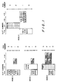
- Fig. 1 illustrates in block forms the memory configurations in their respective systems and the memory contents used therein that can be employed in connection with the invention. As typical examples, four kinds of modes, that is, Mode 0 - Mode 3 are shown in this figure.
- the kinds of RAMs used are determined or varied according to the respective modes, or, Mode 0 - Mode 3, and thus in the prior art techniques four kinds of memory interface circuits which are different from one another are necessary.
- only one memory interface circuit is sufficient for this purpose.
- a ROM 0 32K-byte
- an expansionary ROM 1 (16K-byte) are used in common in the respective modes.
- Mode 0 is a medium-scale standard system that uses a D-RAM element of 16K x 1 bit and is provided with an RAM area of 32K byte.
- Mode 1 is a large-scale system using a D-RAM element of 64K x 1 bit and is provided with an RAM area of 64K byte.
- Mode 2 is a large-scale system which employs 8K-byte CMOS-RAM element or PSEUDO S-RAM and is provided with expandable ROM 2, ROM 3 and ROM 4.
- Mode 3 is a small-scale system which employs an S-RAM element of 2K-byte and is equipped with an expandable ROM 2. This small-scale system can be used in a hand-held personal computer or the like.
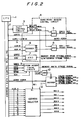
- Fig. 2 is a block diagram of a memory interface circuit of the invention, illustrating a case in which the memory configuration for Mode 0 shown in Fig. 1 is employed.
- a slot control circuit 3 is used to specify slots for each of pages 0 - 3 in Mode 0.
- a ROM 0/ROM 1 access control circuit 4 is used to generate interface signals for ROM 0 (32K bytes for BASIC) and ROM 1 (Expansionary 16K bytes) both of which are commonly used in the respective modes, and this circuit 4 includes AND gates 5, 7, 8 as well as an address decoder 6. It should be noted here that circuits corresponding to this ROM 0/ROM 1 access control circuit 4 are respectively contained in the memory interface circuits of Modes 1, 2 and 3 as well.
- AND gate 5 is used to generate chip select signals of ROM 0
- AND gate 7 is dedicated to generating memory strobe signals
- AND gate 8 is adapted to generate chip select signals of ROM 1.
- the lower half section of Fig. 2 is an interface circuit for a 16K-bit D-RAM used only in Mode 0, and it comprises a D-RAM access timing circuit 9, an AND gate 10, a decoder 11 for generating column address strobe signals and a 7-bit address selector 12 for switching low addresses and column addresses.
- reference character MA designates a low/column address line.
- ROM 0 packaged in Slot #00 in Mode 0 shown in Fig. 1 is to be accessed by the address lines ADR 0 - ADR 14, chip select signals of ROM 0 and memory strobe signals shown in Fig. 2, while Expansionary ROM 1 packaged in Page 1 of Slot #02 in Mode 0 is to be accessed by the address lines ADR 0 - ADR 13, chip select signals of ROM 1 and memory strobe signals shown in Fig. 2.
- the read/write operation of D-RAM is controlled by seven low/column address lines MA 0 - MA 6, a low address strobe signal (which is the same as the above-mentioned memory strobe signal), two column address strobe signals 002, 003, and a memory write strobe signal.
- Column Address Strobe Signal 002 is used when the D-RAM (16K-byte) in Page 2 is to be accessed
- Column Address Strobe Signal 003 is used when the D-RAM (16K-byte) in Page 3 is to be accessed.
- Fig. 3 is a block diagram of the memory interface circuit of the invention, illustrating a case in which the memory configuration for Mode 1 shown in Fig. 1 is employed.
- a CPU 21 there are included a CPU 21 and an address/data/control bus line 22.
- a slot control circuit 23 is used to specify slots for each of Pages 0 - 3 in Mode 1.
- a ROM 0/ROM 1 access control circuit 24 (corresponding exactly to block 4 of Figure 2) is dedicated to generating interface signals for ROM 0 (32K-byte for BASIC) and ROM 1 (Expansionary 16K bytes) both of which are used commonly in the respective modes.
- the lower half section of Fig. 3 constitutes an interface circuit for a 64K-byte D-RAM which is used only in Mode 1.
- it comprises a D-RAM access timing circuit 25, an AND gate 26 for generating column address strobe signals, and an 8-bit address selector 27 for switching low addresses and column addresses.
- the read/write operation of the 64K-byte D-RAM of Slot #01 in Mode 1 is controlled by eight low/column address lines 0 - 7, low address strobe signals, a column address strobe signal 001 and a memory write strobe signal.
- FIG. 4 is a block diagram of the memory interface circuit of the invention, illustrating a case in which the memory configuration for Mode 2 is employed.
- Control circuit 33 corresponds exactly to circuit 4 of Figure 2.
- Fig. 4 The central and lower sections of Fig. 4 constitute a memory interface circuit for CMOS-RAMs 1 - 7 and ROMs 2, 3, 4 which are used only in Mode 2.
- This memory interface circuit comprises an address decoder 34, AND circuits 35, 36, 37 for generating the respective chip select signals 2, 3, 4 of Expansionary ROMs 2, 3, 4, a decoder 38 for generating chip enable signals 0 - 3 for an 8K-byte S-RAM, an inverter 39, and an AND gate 40 for generating a memory write strobe signal.
- Reference numeral 42 designates a refresh timing control circuit to generate a refresh signal for an 8K-byte PSEUDO S-RAM.
- Expansionary ROMs 2, 3, 4 in Mode 2 are respectively accessed by ROM chip select signals 2, 3, 4 outputted respectively from AND Gates 35, 36, 37, fourteen address lines ADRs 0 - 13, and a memory strobe signal.
- the read/write operation of the 8K-byte CMOS-RAM packaged in Slot #01 in Mode 2 is controlled by a signal that is inverted from a signal of Address Line ADR 15 by Inverter 39, a memory read strobe signal, a memory write strobe signal, thirteen address lines ADRs 0 - 12, and four chip enable signals 0 - 4 to be outputted from Decoder 38.
- Fig. 5 illustrates the configuration of a CMOS-RAM (8K-byte) to be connected to the interface line shown in Fig. 4.
- the chip enable signals 0 - 3 of the memory interface are supplied to the chip enable 1 terminal or CE 1 of CMOS-RAM, while the signal of Address Line ADR or the inverted signal thereof is supplied to the chip enable 2 terminal or CE 2 of CMOS-RAM.
- the above-mentioned matrix combination of the terminals CE 1 and CE 2 enables to select a large number of memories with a small number of signals.
- Fig. 6 is a block diagram of the memory interface circuit of the invention, illustrating a case in which the memory configuration for Mode 3 shown in Fig. 1 is employed.
- ROM 0/ROM 1 Access control Circuit 64 (corresponding exactly to circuit 4 of Figure 2) is dedicated to generating interface signals for ROM 0 (32K bytes for BASIC) and ROM 1 (Expansionary 16K bytes) both of which are used commonly in the respective modes.
- the central and lower sections of the memory interface circuit in Fig. 6 constitute an interface circuit for the 2K-byte S-RAM and ROM 2 used only in Mode 3.
- This interface circuit comprises an address decoder 65, an AND gate to generate the chip select signal 2 for ROM 2, an AND gate 67, decoders 68, 69 to generate chip enable signals 0 - 3 and HL 0 - 3 for the 2K-byte S-RAM respectively, and an AND gate 70 to generate a memory write strobe signal.
- Expansion ROM 2 of Page 1 of Slot #03 in Mode3 is accessed by a chip select signal for ROM 2, fourteen address lines ADRs 0 - 13, and a memory read strobe signal.
- the read/write operation of the 2K-byte S-RAMS packaged in Pages 2 and 3 of Slot #01 in Mode 3 are controlled by eleven address lines ADRs 0 - 10, eight chip enable signals 0 - 3 and HL 0 - 3, and a memory write strobe signal.
- Fig. 7 illustrates the configuration of the 2K-byte S-RAM to be connected to the interface line in Fig. 6.
- the chip enable 1 terminal CE 1 of S-RAM is used to connect one of the chip enable signals HL 0 - 3 on the LOW side, while the chip enable 2 terminal CE 2 thereof is used to connect one of the chip enable signals 0 - 3 on the HIGH side.
- the terminals CE 1 and CE 2 can be combined in a matrix manner, so that 16 memories can be selectively specified by 8 chip enable signals.
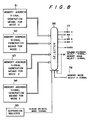
- Fig. 8 illustrates a general block diagram of one embodiment of the memory interface circuit of the invention.
- a memory address signal generation means 91 for Mode 0 there are included a memory address signal generation means 91 for Mode 0, a memory address signal generation means 92 for Mode 1, a memory address signal generation means 93 for Mode 2, a memory address signal generation means 94 for Mode 3, an expansion register 95, and a selector 96.
- the memory address signal generation means 91 for Mode 0 is provided with the same functional operation as the circuit shown in Fig. 2
- the memory address signal generation means 92 is provided with the same functional operation as the circuit shown in Fig. 3
- the memory address signal generation means 93 for Mode 2 is provided with the same functional operation as the circuit shown in Fig. 4
- the memory address signal generation means 94 for Mode 3 is provided with the same functional operation as the circuit shown in Fig. 6.
- Expansion Register 95 is to be established by software and is actually mounted within the multi-function CPU.
- Selector 96 selects one of the outputs of the memory interface circuits in the respective modes according to a memory mode select signal 0 supplied from an external source, a memory mode select signal 1, and an S-RAM 8K-byte mode signal from Expansion Register 95, and then it outputs the selected one as a memory interface signal.
- a memory interface signal necessary for a given mode is selected by Selector 96 and is output to each of memory elements.
- a memory interface signal which is commn in the respective modes is not described here.
- the memory interface signals are selected by a memory select signal 0 externally inputted, the S-RAM 8K-byte mode signal from Expansion Register 95 and the memory select 1 signal common for input and output, while they are output in the form of ten memory interface signals (that is, signals for low/column address lines 0 - 7, a column address 0 signal, and a memory mode select 1 signal).
- Fig. 9 is a table to illustrate the functions of the respective output pins of the memory interface of the invention with respect to the respective modes.
- a memory mode select signal 0 (MMS 0) may be set in the "HIGH”.
- Mode 1 the above memory mode select singal 0 (MMS 0) may be set in the “LOW” and at the same time a memory mode select signal 1 (MMS 1) may be set in the "LOW".
- the memory mode select signal 0 (MMS 0) may be set in the "LOW”
- the memory mode select signal 1 (MMS 1) may be set in the"HIGH”
- an S-RAM 8K-byte mode signal (SR8K) may be set in the "1".
- the memory mode select signal 0 (MMS 0) may be set in the "LOW”
- the memory mode select signal 1 (MMS 1) may be set in the "HIGH”
- the S-RAM 8K-byte mode signal (SR8K) may be set in the "0".
- a terminal for the column address select 1 signal/memory mode select 1 signal shown in Fig. 8 is adapted to operate as a column address strobe signal 003 when the memory mode select signal 0 (MMS 0) is in the "HIGH”, while it is adapted to operate as an input terminal for the memory mode select signal 1 (MMS 1) when the memory mode select signal 0 (MMS 0) is in the "LOW".
- MMS 1 memory mode select signal 1
- four memory address modes can be specified by using an exclusive memory mode select terminal (pin) and an associated remaining terminal (pin).
- the invention is capable of performing the same functions as those of several kinds of memory interface circuits.
- reference character CAS designates a column address select signal
- CSROM represents a chip select signal of ROM
- CERAM denotes a chip enable signal of RAM.
- the present invention is advantageous over the prior art circuits in that various kinds of RAM elements or ROM elements can be directly connected to a multi-function CPU. Thanks to this advantage, since the need to add an external memory access circuit is eliminated, a compact microcomputer sytem can be obtained. Also, according to the invention, the number of terminals or pins required for the above-mentioned functions can be reduced to a minimum.
Landscapes
- Engineering & Computer Science (AREA)
- Theoretical Computer Science (AREA)
- Physics & Mathematics (AREA)
- General Engineering & Computer Science (AREA)
- General Physics & Mathematics (AREA)
- Read Only Memory (AREA)
- Dram (AREA)
Claims (8)
- Circuit d'interface de mémoire destiné à servir dans une unité centrale de traitement CPU multifonction incluant une unité CPU (microprocesseur) (1,21,31,61) et ses éléments de circuit périphériques, caractérisé par une pluralité de moyens générateurs de signaux d'adresse de mémoire et de signaux de commande de mémoire (91,92,93,94) dont chacun est spécifique pour un mode prédéterminé de fonctionnement d'une interface de mémoire et ainsi pour engendrer les signaux d'adresse de mémoire et de commande de mémoire appropriés; et un moyen de sélection de mode (78,95,96) pour sélectionner un de ladite pluralité de moyens générateurs de signaux d'adresse de mémoire et de signaux de commande de mémoire .
- Circuit d'interface de mémoire selon la revendication 1, caractérisé en ce qu'une partie d'une borne incluse dans ledit moyen de sélection de mode (78,95,96) est adaptée pour fournir un signal de sortie dans un mode prédéterminé et, dans les autres modes que ledit mode prédéterminé, pour recevoir un signal d'entrée et également pour spécifier un autre mode.
- Circuit d'interface de mémoire selon la revendication 1, caractérisé en ce que ledit moyen de sélection de mode est constitué d'un registre d'extension (95) prévu à l'intérieur de ladite unité CPU multifonction.
- Circuit d'interface de mémoire selon la revendication 1, caractérisé en ce que lesdits signaux d'adresse de mémoire comprennent un signal d'adresse de mémoire pour une mémoire vive dynamique D-RAM.
- Circuit d'interface de mémoire selon la revendication 1, caractérisé en ce qu'un desdits signaux d'adresse de mémoire sélectionnés par un moyen de sélection de mode (91) peut servir à sélectionner une mémoire parmi une pluralité de mémoires D-RAM.
- Circuit d'interface de mémoire selon la revendication 1, caractérisé en ce qu'un desdits signaux d'adresse de mémoire est un signal de commande d'adressage de mémoire pour une mémoire statique.
- Circuit d'interface de mémoire selon la revendication 1, caractérisé en ce qu'un desdits signaux d'adresse de mémoire sélectionné par un moyen de spécification de mode (94) est un signal d'adresse de mémoire servant à sélectionner une mémoire parmi une pluralité de mémoires statiques.
- Circuit d'interface de mémoire selon la revendication 7, caractérisé en ce que la sélection desdites mémoires statiques est spécifiée sous forme matricielle de telle sorte qu'un grand nombre d'éléments de mémoire peuvent être sélectionnés par la mise en oeuvre d'un petit nombre de bornes.
Applications Claiming Priority (2)
| Application Number | Priority Date | Filing Date | Title |
|---|---|---|---|
| JP6827384A JPS60211555A (ja) | 1984-04-04 | 1984-04-04 | メモリインタフエ−ス回路 |
| JP68273/84 | 1984-04-04 |
Publications (3)
| Publication Number | Publication Date |
|---|---|
| EP0157341A2 EP0157341A2 (fr) | 1985-10-09 |
| EP0157341A3 EP0157341A3 (en) | 1989-08-02 |
| EP0157341B1 true EP0157341B1 (fr) | 1993-06-09 |
Family
ID=13368981
Family Applications (1)
| Application Number | Title | Priority Date | Filing Date |
|---|---|---|---|
| EP19850103569 Expired - Lifetime EP0157341B1 (fr) | 1984-04-04 | 1985-03-26 | Circuit d'interface de mémoire |
Country Status (3)
| Country | Link |
|---|---|
| EP (1) | EP0157341B1 (fr) |
| JP (1) | JPS60211555A (fr) |
| DE (1) | DE3587387T2 (fr) |
Families Citing this family (3)
| Publication number | Priority date | Publication date | Assignee | Title |
|---|---|---|---|---|
| JPS63647A (ja) * | 1986-06-19 | 1988-01-05 | Fujitsu Ltd | メモリ領域切換回路 |
| JPS63257859A (ja) * | 1987-04-15 | 1988-10-25 | Matsushita Electric Ind Co Ltd | メモリ制御装置 |
| US5036495A (en) * | 1989-12-28 | 1991-07-30 | International Business Machines Corp. | Multiple mode-set for IC chip |
Family Cites Families (2)
| Publication number | Priority date | Publication date | Assignee | Title |
|---|---|---|---|---|
| US4475176A (en) * | 1981-08-06 | 1984-10-02 | Tokyo Shibaura Denki Kabushiki Kaisha | Memory control system |
| JPS5952483A (ja) * | 1982-09-17 | 1984-03-27 | Fujitsu Ltd | 主記憶装置 |
-
1984
- 1984-04-04 JP JP6827384A patent/JPS60211555A/ja active Pending
-
1985
- 1985-03-26 EP EP19850103569 patent/EP0157341B1/fr not_active Expired - Lifetime
- 1985-03-26 DE DE19853587387 patent/DE3587387T2/de not_active Expired - Fee Related
Also Published As
| Publication number | Publication date |
|---|---|
| DE3587387D1 (de) | 1993-07-15 |
| DE3587387T2 (de) | 1993-11-18 |
| JPS60211555A (ja) | 1985-10-23 |
| EP0157341A3 (en) | 1989-08-02 |
| EP0157341A2 (fr) | 1985-10-09 |
Similar Documents
| Publication | Publication Date | Title |
|---|---|---|
| US4566082A (en) | Memory pack addressing system | |
| EP0183231B1 (fr) | Processeur de données | |
| KR940002754B1 (ko) | 반도체 집적회로 장치의 제어방법 | |
| US4831522A (en) | Circuit and method for page addressing read only memory | |
| US4694394A (en) | Microprocessor system having a multiplexed address/data bus which communicates with a plurality of memory and input/output devices including TTL output gates | |
| US4319343A (en) | Programmable digital memory circuit | |
| US5019970A (en) | IC card | |
| US5025415A (en) | Memory card | |
| US5339402A (en) | System for connecting an IC memory card to a central processing unit of a computer | |
| US4918586A (en) | Extended memory device with instruction read from first control store containing information for accessing second control store | |
| EP0157341B1 (fr) | Circuit d'interface de mémoire | |
| US5373467A (en) | Solid state memory device capable of providing data signals on 2N data lines or N data lines | |
| US5179676A (en) | Address selection circuit including address counters for performing address selection | |
| US5263141A (en) | Microprocessor with an exclusive address terminal for selecting at least one part of a peripheral device | |
| EP0262413B1 (fr) | Dispositif de mémoire à multiplexage d'adresses | |
| JPH05210577A (ja) | チップ選択端子対を備える半導体装置 | |
| US5396611A (en) | Microprocessor use in in-circuit emulator having function of discriminating user's space and in-circuit emulator space | |
| JPH1139212A (ja) | マイクロコンピュータ | |
| JPH1153338A (ja) | 半導体集積回路およびその半導体集積回路における外部バスモード選択方法 | |
| KR0161487B1 (ko) | 메모리 컨트롤 회로 | |
| KR890003234Y1 (ko) | 다이나믹램의 타입에 따른 메모리뱅크 선택변환회로 | |
| KR950000124B1 (ko) | 다이나믹형 메모리의 액세스 방법 및 데이타 처리 시스템의 구축 방법과 데이타 처리 시스템 | |
| JPH11149334A (ja) | バス信号制御回路 | |
| JP3336624B2 (ja) | 評価用データ処理半導体装置のアクセス対象選択回路 | |
| JPS60114954A (ja) | 超小形計算機 |
Legal Events
| Date | Code | Title | Description |
|---|---|---|---|
| PUAI | Public reference made under article 153(3) epc to a published international application that has entered the european phase |
Free format text: ORIGINAL CODE: 0009012 |
|
| 17P | Request for examination filed |
Effective date: 19850326 |
|
| AK | Designated contracting states |
Designated state(s): DE FR GB NL |
|
| PUAL | Search report despatched |
Free format text: ORIGINAL CODE: 0009013 |
|
| AK | Designated contracting states |
Kind code of ref document: A3 Designated state(s): DE FR GB NL |
|
| 17Q | First examination report despatched |
Effective date: 19910724 |
|
| GRAA | (expected) grant |
Free format text: ORIGINAL CODE: 0009210 |
|
| AK | Designated contracting states |
Kind code of ref document: B1 Designated state(s): DE FR GB NL |
|
| REF | Corresponds to: |
Ref document number: 3587387 Country of ref document: DE Date of ref document: 19930715 |
|
| ET | Fr: translation filed | ||
| PLBE | No opposition filed within time limit |
Free format text: ORIGINAL CODE: 0009261 |
|
| STAA | Information on the status of an ep patent application or granted ep patent |
Free format text: STATUS: NO OPPOSITION FILED WITHIN TIME LIMIT |
|
| 26N | No opposition filed | ||
| REG | Reference to a national code |
Ref country code: GB Ref legal event code: IF02 |
|
| PGFP | Annual fee paid to national office [announced via postgrant information from national office to epo] |
Ref country code: GB Payment date: 20020206 Year of fee payment: 18 |
|
| PGFP | Annual fee paid to national office [announced via postgrant information from national office to epo] |
Ref country code: FR Payment date: 20020318 Year of fee payment: 18 |
|
| PGFP | Annual fee paid to national office [announced via postgrant information from national office to epo] |
Ref country code: DE Payment date: 20020326 Year of fee payment: 18 |
|
| PGFP | Annual fee paid to national office [announced via postgrant information from national office to epo] |
Ref country code: NL Payment date: 20020331 Year of fee payment: 18 |
|
| PG25 | Lapsed in a contracting state [announced via postgrant information from national office to epo] |
Ref country code: GB Free format text: LAPSE BECAUSE OF NON-PAYMENT OF DUE FEES Effective date: 20030326 |
|
| PG25 | Lapsed in a contracting state [announced via postgrant information from national office to epo] |
Ref country code: NL Free format text: LAPSE BECAUSE OF NON-PAYMENT OF DUE FEES Effective date: 20031001 Ref country code: DE Free format text: LAPSE BECAUSE OF NON-PAYMENT OF DUE FEES Effective date: 20031001 |
|
| GBPC | Gb: european patent ceased through non-payment of renewal fee |
Effective date: 20030326 |
|
| PG25 | Lapsed in a contracting state [announced via postgrant information from national office to epo] |
Ref country code: FR Free format text: LAPSE BECAUSE OF NON-PAYMENT OF DUE FEES Effective date: 20031127 |
|
| NLV4 | Nl: lapsed or anulled due to non-payment of the annual fee |
Effective date: 20031001 |
|
| REG | Reference to a national code |
Ref country code: FR Ref legal event code: ST |