EP0157505A2 - Dispositif semi-conducteur à haute fréquence - Google Patents
Dispositif semi-conducteur à haute fréquence Download PDFInfo
- Publication number
- EP0157505A2 EP0157505A2 EP85301547A EP85301547A EP0157505A2 EP 0157505 A2 EP0157505 A2 EP 0157505A2 EP 85301547 A EP85301547 A EP 85301547A EP 85301547 A EP85301547 A EP 85301547A EP 0157505 A2 EP0157505 A2 EP 0157505A2
- Authority
- EP
- European Patent Office
- Prior art keywords
- container
- circuit
- semiconductor device
- supplementary
- input
- Prior art date
- Legal status (The legal status is an assumption and is not a legal conclusion. Google has not performed a legal analysis and makes no representation as to the accuracy of the status listed.)
- Granted
Links
Images

Classifications
-
- H—ELECTRICITY
- H10—SEMICONDUCTOR DEVICES; ELECTRIC SOLID-STATE DEVICES NOT OTHERWISE PROVIDED FOR
- H10W—GENERIC PACKAGES, INTERCONNECTIONS, CONNECTORS OR OTHER CONSTRUCTIONAL DETAILS OF DEVICES COVERED BY CLASS H10
- H10W76/00—Containers; Fillings or auxiliary members therefor; Seals
- H10W76/10—Containers or parts thereof
- H10W76/12—Containers or parts thereof characterised by their shape
- H10W76/13—Containers comprising a conductive base serving as an interconnection
- H10W76/134—Containers comprising a conductive base serving as an interconnection having other interconnections parallel to the conductive base
-
- H—ELECTRICITY
- H10—SEMICONDUCTOR DEVICES; ELECTRIC SOLID-STATE DEVICES NOT OTHERWISE PROVIDED FOR
- H10W—GENERIC PACKAGES, INTERCONNECTIONS, CONNECTORS OR OTHER CONSTRUCTIONAL DETAILS OF DEVICES COVERED BY CLASS H10
- H10W44/00—Electrical arrangements for controlling or matching impedance
- H10W44/20—Electrical arrangements for controlling or matching impedance at high-frequency [HF] or radio frequency [RF]
-
- H—ELECTRICITY
- H10—SEMICONDUCTOR DEVICES; ELECTRIC SOLID-STATE DEVICES NOT OTHERWISE PROVIDED FOR
- H10W—GENERIC PACKAGES, INTERCONNECTIONS, CONNECTORS OR OTHER CONSTRUCTIONAL DETAILS OF DEVICES COVERED BY CLASS H10
- H10W70/00—Package substrates; Interposers; Redistribution layers [RDL]
- H10W70/60—Insulating or insulated package substrates; Interposers; Redistribution layers
- H10W70/67—Insulating or insulated package substrates; Interposers; Redistribution layers characterised by their insulating layers or insulating parts
- H10W70/68—Shapes or dispositions thereof
- H10W70/682—Shapes or dispositions thereof comprising holes having chips therein
Definitions
- the present invention relates to a semiconductor device, and more particularly, but not exclusively,to an improvement in a container for housing a high-frequency semiconductor circuit using a radio-frequency wave such as a microwave or a millimeter wave.
- a previously proposed semiconductor device having a microwave circuit housed within a ceramic container suffers from degradation of circuit characteristics due to the frequency resonance of the container and from damage of the container due to the difference of the thermal expansion coefficients of the ceramic and the metal base plate.
- radio waves propagate from the input side to the output side within the container space, which causes undesired characteristics, e.g. noise on the output signal.
- the impedance of a part of the circuit matches the impedance of the space within the container, which impedance is usually very high.
- This causes radiation of the microwave from the input side within the container, resulting in so-called rectangular waveguide mode signal progagation within the container. Therefore, the undesirable wave propagation occurs at a frequency which is used in the circuit of the container.
- the cutoff frequency of the waveguide within the container must be higher than the frequency of the signal used in the circuit, since the waveguide functions as a high-pass filter. That is, the length of the longer side of the cross-section of the container inner space must be. shortened according to the frequency of the signal.
- the container requires supplementary space for handling parts of the microwave circuit in addition to and adjacent to the space for mounting the microwave circuit on the container bottom surface. Also, supplementary space is necessary for mounting parts of, for instance, a DC bias circuit of the microcircuit.
- radio frequency semiconductor device in which the above-mentioned problems are solved, so that it can be used at a desired high frequency without degrading the high frequency characteristics and so that sufficient supplementary space is maintained around the semiconductor circuit for mounting electric components of a supplementary circuit such as a bias circuit or DC power supply circuit and handling the parts when mounting the semiconductor circuit, such as a microwave circuit.
- a supplementary circuit such as a bias circuit or DC power supply circuit
- a semiconductor device including a metallic container for containing a radio frequency semiconductor circuit on a bottom surface thereof; a cap for covering the container; and input and output terminals connected to the circuit and penetrating through a side wall of the container at locations Opposite to each other.
- the bottom surface includes space for mounting the radio frequency semiconductor circuit and supplementary space for mounting elements of a supplementary circuit.
- Means for increasing the cutoff frequency of the waveguide mode wave propagation between the input and output terminals within the container is provided on a part of the supplementary space, so that the cutoff frequency is higher than the wave frequency used in the radio frequency semiconductor circuit.
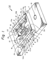
- a first embodiment of the present invention is illustrated in Figs. 1 and 2.
- a metallic container 30 for containing a microwave circuit 3 therein includes a metallic base plate 1 and side walls 2a and 2b forming an essentially rectangular shape on the base plate 1 and accommodating the microwave circuit 3 therein..
- a cap 19 (Fig. 2(B)) is disposed on the side walls 2a, 2b for covering the container 30.
- the container 30 is made of a metal such as copper.
- the cap 19 is made of metal or ceramic having a metallized surface.
- a hole 18 for attaching the container 30 to another location is provided on the base plate 1.
- the microwave circuit 3 is a strip line type circuit and includes, for example, a pair of ceramic plates 4, on which a matching circuit pattern 5 is printed and a DC blocking capacitor 6 is mounted, and a field effect transistor (FET) 7 and capacitors 8 disposed between the ceramic plates 4, to constitute a single end type amplifier.
- the parts are connected to each other by wires (not shown).
- Capacitors 17, which constitute a supplementary bias circuit for DC power supply or ground connection, are mounted beside the microwave circuit 3 and connected thereto by wires (not shown). Therefore, the bottom surface inside of the side walls 2a, 2b of the container 30 requires not only space 31 (Fig. 2) for mounting the microwave circuit 3 but also supplementary space 16 for mounting electric components for a supplementary circuit such as a bias circuit. Such a supplementary space 16 is also required as space for handling elements of the microwave circuit 3 when mounting it on the bottom surface of the container 30.
- Three terminals 12 are disposed on one side of the side wall 2a and three other terminals are disposed on the opposite side of the side wall 2a. Each terminal 12 penetrates through the side wall 2a so as to interconnect the inner circuits and outer lines (not shown). Each terminal 12 is surrounded by ceramic 11 to be isolated from the side wall 2a. The size of the ceramic 11 is determined considering the impedance matching characteristic thereof corresponding to the impedance of the inner circuit. Steps 9, 10 having a thickness corresponding to the thickness of the ceramic plate 4 are formed on the inner and outer sides of the side wall 2a. Each terminal 12 is exposed on the ceramic 11 on the steps 9 and 10.
- Leads 13a and 13b designate a radio frequency wave input lead and output lead, respectively.
- Leads 14a and 14b designate DC input and output leads, respectively.
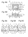
- Metallized film may be formed on the ceramic 11 from the inner step 9 to the outer step 10 penetrating the side wall 2a to constitute a terminal 12. With such a structure, the outer projecting leads 13a, 13b, 14a, 14b may be deleted, as illustrated in Fig. 4(A). If a radio frequency wave circuit using a self-bias FET or a diode is housed in the container, the number of the DC terminals may be one on each side.
- a projection 15 is formed inward of and integral with each side wall 2b on each side perpendicular to the side wall 2a having the terminals 12.
- the projection 15 extends in height between the lower surface of the cap 19 and the bottom surface of the container.
- the projection 15 functions as a filter of the radio wave propagating within the container in a waveguide mode.
- the metal container 30 functions as a rectangular waveguide with the cap 19.
- the cutoff wavelength of the waveguide mode wave propagating within the container from the input terminal lead 13a to the output terminal lead 13b mainly depends on the length of the longer side of the waveguide section, i.e., the length of the cross-section parallel to the side wall 2a having terminals. That length is the length (1) between the projections 15 which is shorter than the length ,(L), which is the length to determine the cutoff wavelength in the case where the projections 15 are not provided. Therefore, the cutoff wavelength is shortened by projections 15 which means the cutoff frequency is increased.
- the waveguide functions as a high-pass filter. Therefore, by arranging the length (l) so that the cutoff frequency is higher than the wave frequency used in the microwave circuit, waveguide mode propagation of - the wave having the frequency of the microwave circuit does not occur. Accordingly, no wave propagation occurs so that all of the input high frequency signal is introduced into the microwave circuit 3 from the input terminal lead 13a and transmitted to the output terminal lead 13b. Therefore, noise due to the wave propagation of the waveguide mode and transmission loss are minimized and the circuit characteristics are stabilized. Also, it is possible to use a very high frequency wave by providing an appropriate size projection 15.
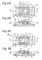
- a second embodiment of the present invention is illustrated in Fig. 3.
- metallic projections 20 which are separated from the side wall 2b are provided as cutoff means for filtering the waveguide mode propagation of the radio wave, instead of.the projection 15 of the first embodiment.
- the other constructions, functions, and effects of the structure are substantially the same as those of the first embodiment.
- the space between the projections 20 and the side wall 2b is also utilized as supplementary space.
- a third embodiment is illustrated in Fig. 4.
- the projection 15 arranged similarly to the structure of the first embodiment has a terminal 21 surrounded by ceramic 11 and penetrating through the projection.
- the outer leads 13a, 13b, 14a, 14b do not project out of the container edge.
- the other constructions, functions, and effects are substantially the same as those of the first embodiment.
- the electric components disposed in the supplementary space 16 on the opposite sides of the projection 15 can be easily connected to each other by using the terminal 21 penetrating through the projection 15. Also, it is convenient to dispose a plurality of the containers side by side closely in parallel, since the leads are not projected out of the side wall of the container.
- cutoff members 22 are formed on both sides of the space 31 for mounting a radio frequency semiconductor circuit such as a microwave circuit 3, leaving the supplementary space 16 as in the above-mentioned embodiments.
- the cutoff members 22 shorten the length of the long side of the container, which length determines the cutoff frequency of the waveguide mode wave propagation from (L) to (t).
- Figure 6 is an upper view of the arrangement of four semiconductor devices of the present invention disposed close together side by side and connected to each other through the terminals 13a, 13b, 14a, 14b of each container 30. With such an arrangement, a plurality of semiconductor devices having stable characteristics and using a desired high frequency can be compactly interconnected.
Landscapes
- Waveguides (AREA)
- Microwave Amplifiers (AREA)
Applications Claiming Priority (2)
| Application Number | Priority Date | Filing Date | Title |
|---|---|---|---|
| JP59042605A JPS60210853A (ja) | 1984-03-06 | 1984-03-06 | 半導体装置 |
| JP42605/84 | 1984-03-06 |
Publications (3)
| Publication Number | Publication Date |
|---|---|
| EP0157505A2 true EP0157505A2 (fr) | 1985-10-09 |
| EP0157505A3 EP0157505A3 (en) | 1987-04-15 |
| EP0157505B1 EP0157505B1 (fr) | 1991-10-09 |
Family
ID=12640670
Family Applications (1)
| Application Number | Title | Priority Date | Filing Date |
|---|---|---|---|
| EP85301547A Expired - Lifetime EP0157505B1 (fr) | 1984-03-06 | 1985-03-06 | Dispositif semi-conducteur à haute fréquence |
Country Status (5)
| Country | Link |
|---|---|
| US (1) | US4713634A (fr) |
| EP (1) | EP0157505B1 (fr) |
| JP (1) | JPS60210853A (fr) |
| KR (1) | KR900008206B1 (fr) |
| DE (1) | DE3584301D1 (fr) |
Cited By (6)
| Publication number | Priority date | Publication date | Assignee | Title |
|---|---|---|---|---|
| EP0387955A1 (fr) * | 1989-03-17 | 1990-09-19 | Laboratoires D'electronique Philips | Boîtier pour circuit intégré hyperfréquences |
| EP0441180A1 (fr) * | 1989-01-09 | 1991-08-14 | Mitsubishi Denki Kabushiki Kaisha | Circuit intégré contenant des circuits à micro-ondes |
| US5136271A (en) * | 1989-01-09 | 1992-08-04 | Mitsubishi Denki Kabushiki Kaisha | Microwave integrated circuit mountings |
| EP0552701A3 (en) * | 1992-01-24 | 1993-09-01 | Sumitomo Electric Industries, Ltd. | Package for microwave device |
| US5889319A (en) * | 1996-07-19 | 1999-03-30 | Ericsson, Inc. | RF power package with a dual ground |
| US6225696B1 (en) * | 1997-09-18 | 2001-05-01 | Trw Inc. | Advanced RF electronics package |
Families Citing this family (20)
| Publication number | Priority date | Publication date | Assignee | Title |
|---|---|---|---|---|
| US4922325A (en) * | 1987-10-02 | 1990-05-01 | American Telephone And Telegraph Company | Multilayer ceramic package with high frequency connections |
| US5075867A (en) * | 1988-12-23 | 1991-12-24 | Bull Hn Information Systems Inc. | Method for limiting spurious resonant cavity effects in electronic equipment |
| US4972043A (en) * | 1989-01-30 | 1990-11-20 | Ixys Corporation | Multi-lead hermetic power package with high packing density |
| US5109594A (en) * | 1990-11-01 | 1992-05-05 | Explosive Fabricators, Inc. | Method of making a sealed transition joint |
| US5376909A (en) * | 1992-05-29 | 1994-12-27 | Texas Instruments Incorporated | Device packaging |
| US5389904A (en) * | 1992-09-11 | 1995-02-14 | Industrial Technology Research Institute, Taiwan, R.O.C. | Surface-mountable, frequency selective microwave IC package |
| DE4331864A1 (de) * | 1993-09-20 | 1995-03-23 | Heidelberger Druckmasch Ag | Gehäuse für ein elektrisches System zum Steuern oder Regeln von Betriebsvorgängen |
| US5650760A (en) * | 1995-11-13 | 1997-07-22 | Hughes Aircraft Company | Microwave enclosure |
| US5774342A (en) * | 1996-09-26 | 1998-06-30 | Delco Electronics Corporation | Electronic circuit with integrated terminal pins |
| FR2776435B1 (fr) * | 1998-03-19 | 2000-04-28 | Alsthom Cge Alcatel | Amplificateur a grand gain |
| JP2000058691A (ja) | 1998-08-07 | 2000-02-25 | Sharp Corp | ミリ波半導体装置 |
| US6441697B1 (en) * | 1999-01-27 | 2002-08-27 | Kyocera America, Inc. | Ultra-low-loss feedthrough for microwave circuit package |
| JP3929197B2 (ja) * | 1999-03-17 | 2007-06-13 | 松下電器産業株式会社 | 高周波回路素子 |
| JP3438132B2 (ja) * | 1999-04-23 | 2003-08-18 | 富士通カンタムデバイス株式会社 | 高周波デバイス用パッケージ |
| JP3328235B2 (ja) | 1999-08-17 | 2002-09-24 | 山形日本電気株式会社 | 半導体装置用セラミックパッケージ |
| JP2003086723A (ja) * | 2001-09-14 | 2003-03-20 | Nec Schott Components Corp | 薄型金属パッケージ |
| US6771147B2 (en) * | 2001-12-17 | 2004-08-03 | Remec, Inc. | 1-100 GHz microstrip filter |
| US7227758B2 (en) * | 2003-07-21 | 2007-06-05 | Delphi Technologies, Inc. | Printed circuit board assembly with integrated connector |
| JP4817924B2 (ja) * | 2006-03-29 | 2011-11-16 | 株式会社東芝 | 半導体パッケージ |
| US10110185B2 (en) * | 2016-09-16 | 2018-10-23 | Kabushiki Kaisha Toshiba | Microwave semiconductor device |
Family Cites Families (11)
| Publication number | Priority date | Publication date | Assignee | Title |
|---|---|---|---|---|
| US2673962A (en) * | 1949-01-18 | 1954-03-30 | Bell Telephone Labor Inc | Mode suppression in curved waveguide bends |
| NL7314268A (nl) * | 1973-10-17 | 1975-04-21 | Philips Nv | Microgolfinrichting in microstripuitvoering. |
| JPS5310948A (en) * | 1976-07-16 | 1978-01-31 | Mitsubishi Electric Corp | Microwave integrated circuit device |
| JPS5366588A (en) * | 1976-11-26 | 1978-06-14 | Fujitsu Ltd | Mounting structure for microstrip printing board |
| JPS5368890A (en) * | 1976-12-01 | 1978-06-19 | Mitsubishi Electric Corp | Suspended line type microwave circuit |
| JPS596513B2 (ja) * | 1978-12-28 | 1984-02-13 | 富士通株式会社 | マイクロ波装置モジユ−ル |
| US4480290A (en) * | 1979-07-17 | 1984-10-30 | Les Condensateurs Sic Safco | Electrolytic capacitor including a composite separator between the anode and the cathode thereof |
| JPS5640263A (en) * | 1979-09-11 | 1981-04-16 | Nec Corp | Package for semiconductor element |
| US4270106A (en) * | 1979-11-07 | 1981-05-26 | The United States Of America As Represented By The Secretary Of The Air Force | Broadband mode suppressor for microwave integrated circuits |
| JPS583922A (ja) * | 1981-06-29 | 1983-01-10 | Kawasaki Steel Corp | 時効性に優れるt−3級ぶりき板の製造方法 |
| JPS58190046A (ja) * | 1982-04-30 | 1983-11-05 | Fujitsu Ltd | 半導体装置 |
-
1984
- 1984-03-06 JP JP59042605A patent/JPS60210853A/ja not_active Expired - Lifetime
-
1985
- 1985-03-05 US US06/708,609 patent/US4713634A/en not_active Expired - Lifetime
- 1985-03-06 KR KR1019850001407A patent/KR900008206B1/ko not_active Expired
- 1985-03-06 DE DE8585301547T patent/DE3584301D1/de not_active Expired - Lifetime
- 1985-03-06 EP EP85301547A patent/EP0157505B1/fr not_active Expired - Lifetime
Cited By (9)
| Publication number | Priority date | Publication date | Assignee | Title |
|---|---|---|---|---|
| EP0441180A1 (fr) * | 1989-01-09 | 1991-08-14 | Mitsubishi Denki Kabushiki Kaisha | Circuit intégré contenant des circuits à micro-ondes |
| US5136271A (en) * | 1989-01-09 | 1992-08-04 | Mitsubishi Denki Kabushiki Kaisha | Microwave integrated circuit mountings |
| EP0387955A1 (fr) * | 1989-03-17 | 1990-09-19 | Laboratoires D'electronique Philips | Boîtier pour circuit intégré hyperfréquences |
| FR2644631A1 (fr) * | 1989-03-17 | 1990-09-21 | Labo Electronique Physique | Boitier pour circuit integre hyperfrequences |
| EP0552701A3 (en) * | 1992-01-24 | 1993-09-01 | Sumitomo Electric Industries, Ltd. | Package for microwave device |
| US5416660A (en) * | 1992-01-24 | 1995-05-16 | Sumitomo Electric Industries, Ltd. | Package for microwave device |
| US5889319A (en) * | 1996-07-19 | 1999-03-30 | Ericsson, Inc. | RF power package with a dual ground |
| US6225696B1 (en) * | 1997-09-18 | 2001-05-01 | Trw Inc. | Advanced RF electronics package |
| US6261872B1 (en) | 1997-09-18 | 2001-07-17 | Trw Inc. | Method of producing an advanced RF electronic package |
Also Published As
| Publication number | Publication date |
|---|---|
| KR850006779A (ko) | 1985-10-16 |
| DE3584301D1 (de) | 1991-11-14 |
| US4713634A (en) | 1987-12-15 |
| EP0157505B1 (fr) | 1991-10-09 |
| KR900008206B1 (ko) | 1990-11-05 |
| EP0157505A3 (en) | 1987-04-15 |
| JPS60210853A (ja) | 1985-10-23 |
Similar Documents
| Publication | Publication Date | Title |
|---|---|---|
| EP0157505A2 (fr) | Dispositif semi-conducteur à haute fréquence | |
| EP0438056B1 (fr) | Boîtier pour circuit haute-fréquence | |
| JPH05114803A (ja) | 高周波フイルタおよびその製法 | |
| US4768004A (en) | Electrical circuit interconnect system | |
| JPH0220158B2 (fr) | ||
| US6087912A (en) | High frequency multi-layer module comprising a dielectric resonator | |
| EP0498893B1 (fr) | Amplificateur hyperfrequence a plusieurs etages | |
| JPH09321501A (ja) | 多層高周波回路基板 | |
| US4906957A (en) | Electrical circuit interconnect system | |
| JPH0340961B2 (fr) | ||
| JP3821630B2 (ja) | 高周波シールド構造 | |
| JPH056922B2 (fr) | ||
| JP2586817B2 (ja) | 混成集積回路装置 | |
| JP3961744B2 (ja) | マイクロ波モジュール | |
| JP4074839B2 (ja) | 誘電体導波管共振器の入出力結合構造とそれを利用した発振器 | |
| US4516271A (en) | Microwave mixer with recovery of the sum frequency | |
| JP2589597B2 (ja) | 誘電体共振器及びそれを用いた帯域阻止フィルタ | |
| US6531934B1 (en) | Dielectric resonator, dielectric filter, dielectric duplexer, oscillator, and communication device | |
| JPS6326921B2 (fr) | ||
| JPS58123201A (ja) | マイクロ波回路の遮蔽構造 | |
| JP2001136008A (ja) | マイクロ波導波管装置 | |
| JP3127645B2 (ja) | パッケージ構造 | |
| JPH01212456A (ja) | 半導体装置用パッケージ | |
| JPH05110310A (ja) | マイクロ波回路 | |
| JP3981506B2 (ja) | 高周波パッケージ |
Legal Events
| Date | Code | Title | Description |
|---|---|---|---|
| PUAI | Public reference made under article 153(3) epc to a published international application that has entered the european phase |
Free format text: ORIGINAL CODE: 0009012 |
|
| AK | Designated contracting states |
Designated state(s): DE FR GB IT SE |
|
| PUAL | Search report despatched |
Free format text: ORIGINAL CODE: 0009013 |
|
| AK | Designated contracting states |
Kind code of ref document: A3 Designated state(s): DE FR GB IT SE |
|
| 17P | Request for examination filed |
Effective date: 19871006 |
|
| 17Q | First examination report despatched |
Effective date: 19890905 |
|
| ITF | It: translation for a ep patent filed | ||
| GRAA | (expected) grant |
Free format text: ORIGINAL CODE: 0009210 |
|
| AK | Designated contracting states |
Kind code of ref document: B1 Designated state(s): DE FR GB IT SE |
|
| REF | Corresponds to: |
Ref document number: 3584301 Country of ref document: DE Date of ref document: 19911114 |
|
| ET | Fr: translation filed | ||
| PLBE | No opposition filed within time limit |
Free format text: ORIGINAL CODE: 0009261 |
|
| STAA | Information on the status of an ep patent application or granted ep patent |
Free format text: STATUS: NO OPPOSITION FILED WITHIN TIME LIMIT |
|
| 26N | No opposition filed | ||
| EAL | Se: european patent in force in sweden |
Ref document number: 85301547.7 |
|
| PGFP | Annual fee paid to national office [announced via postgrant information from national office to epo] |
Ref country code: SE Payment date: 19980317 Year of fee payment: 14 |
|
| PG25 | Lapsed in a contracting state [announced via postgrant information from national office to epo] |
Ref country code: SE Free format text: LAPSE BECAUSE OF NON-PAYMENT OF DUE FEES Effective date: 19990307 |
|
| EUG | Se: european patent has lapsed |
Ref document number: 85301547.7 |
|
| EUG | Se: european patent has lapsed |
Ref document number: 85301547.7 |
|
| REG | Reference to a national code |
Ref country code: GB Ref legal event code: IF02 |
|
| PGFP | Annual fee paid to national office [announced via postgrant information from national office to epo] |
Ref country code: GB Payment date: 20030305 Year of fee payment: 19 |
|
| PGFP | Annual fee paid to national office [announced via postgrant information from national office to epo] |
Ref country code: FR Payment date: 20030310 Year of fee payment: 19 |
|
| PGFP | Annual fee paid to national office [announced via postgrant information from national office to epo] |
Ref country code: DE Payment date: 20030313 Year of fee payment: 19 |
|
| PG25 | Lapsed in a contracting state [announced via postgrant information from national office to epo] |
Ref country code: GB Free format text: LAPSE BECAUSE OF NON-PAYMENT OF DUE FEES Effective date: 20040306 |
|
| PG25 | Lapsed in a contracting state [announced via postgrant information from national office to epo] |
Ref country code: DE Free format text: LAPSE BECAUSE OF NON-PAYMENT OF DUE FEES Effective date: 20041001 |
|
| GBPC | Gb: european patent ceased through non-payment of renewal fee | ||
| PG25 | Lapsed in a contracting state [announced via postgrant information from national office to epo] |
Ref country code: FR Free format text: LAPSE BECAUSE OF NON-PAYMENT OF DUE FEES Effective date: 20041130 |
|
| REG | Reference to a national code |
Ref country code: FR Ref legal event code: ST |