EP0157524A2 - Panneau plat d'affichage - Google Patents
Panneau plat d'affichage Download PDFInfo
- Publication number
- EP0157524A2 EP0157524A2 EP85301823A EP85301823A EP0157524A2 EP 0157524 A2 EP0157524 A2 EP 0157524A2 EP 85301823 A EP85301823 A EP 85301823A EP 85301823 A EP85301823 A EP 85301823A EP 0157524 A2 EP0157524 A2 EP 0157524A2
- Authority
- EP
- European Patent Office
- Prior art keywords
- display
- electrodes
- signals
- panel
- electrode
- Prior art date
- Legal status (The legal status is an assumption and is not a legal conclusion. Google has not performed a legal analysis and makes no representation as to the accuracy of the status listed.)
- Withdrawn
Links
- 239000011159 matrix material Substances 0.000 claims abstract description 8
- 239000004973 liquid crystal related substance Substances 0.000 claims description 10
- 239000000463 material Substances 0.000 claims description 6
- 230000003068 static effect Effects 0.000 abstract description 6
- 230000003287 optical effect Effects 0.000 abstract description 5
- 230000000694 effects Effects 0.000 description 3
- 238000004519 manufacturing process Methods 0.000 description 3
- 238000000034 method Methods 0.000 description 3
- 230000005540 biological transmission Effects 0.000 description 2
- 230000002459 sustained effect Effects 0.000 description 2
- 230000003098 cholesteric effect Effects 0.000 description 1
- 238000010276 construction Methods 0.000 description 1
- 238000005516 engineering process Methods 0.000 description 1
- 238000003384 imaging method Methods 0.000 description 1
- 230000010354 integration Effects 0.000 description 1
- 238000002372 labelling Methods 0.000 description 1
- 238000005259 measurement Methods 0.000 description 1
- 230000004048 modification Effects 0.000 description 1
- 238000012986 modification Methods 0.000 description 1
- 239000000382 optic material Substances 0.000 description 1
- 239000004065 semiconductor Substances 0.000 description 1
- 229910052710 silicon Inorganic materials 0.000 description 1
- 239000010703 silicon Substances 0.000 description 1
- 239000007787 solid Substances 0.000 description 1
- 230000001960 triggered effect Effects 0.000 description 1
Images


Classifications
-
- G—PHYSICS
- G09—EDUCATION; CRYPTOGRAPHY; DISPLAY; ADVERTISING; SEALS
- G09G—ARRANGEMENTS OR CIRCUITS FOR CONTROL OF INDICATING DEVICES USING STATIC MEANS TO PRESENT VARIABLE INFORMATION
- G09G3/00—Control arrangements or circuits, of interest only in connection with visual indicators other than cathode-ray tubes
- G09G3/001—Control arrangements or circuits, of interest only in connection with visual indicators other than cathode-ray tubes using specific devices not provided for in groups G09G3/02 - G09G3/36, e.g. using an intermediate record carrier such as a film slide; Projection systems; Display of non-alphanumerical information, solely or in combination with alphanumerical information, e.g. digital display on projected diapositive as background
-
- G—PHYSICS
- G09—EDUCATION; CRYPTOGRAPHY; DISPLAY; ADVERTISING; SEALS
- G09G—ARRANGEMENTS OR CIRCUITS FOR CONTROL OF INDICATING DEVICES USING STATIC MEANS TO PRESENT VARIABLE INFORMATION
- G09G3/00—Control arrangements or circuits, of interest only in connection with visual indicators other than cathode-ray tubes
- G09G3/20—Control arrangements or circuits, of interest only in connection with visual indicators other than cathode-ray tubes for presentation of an assembly of a number of characters, e.g. a page, by composing the assembly by combination of individual elements arranged in a matrix no fixed position being assigned to or needed to be assigned to the individual characters or partial characters
- G09G3/34—Control arrangements or circuits, of interest only in connection with visual indicators other than cathode-ray tubes for presentation of an assembly of a number of characters, e.g. a page, by composing the assembly by combination of individual elements arranged in a matrix no fixed position being assigned to or needed to be assigned to the individual characters or partial characters by control of light from an independent source
- G09G3/36—Control arrangements or circuits, of interest only in connection with visual indicators other than cathode-ray tubes for presentation of an assembly of a number of characters, e.g. a page, by composing the assembly by combination of individual elements arranged in a matrix no fixed position being assigned to or needed to be assigned to the individual characters or partial characters by control of light from an independent source using liquid crystals
- G09G3/3611—Control of matrices with row and column drivers
- G09G3/3622—Control of matrices with row and column drivers using a passive matrix
- G09G3/3625—Control of matrices with row and column drivers using a passive matrix using active addressing
Definitions
- the present invention concerns a flat-panel display, in particular a display for use as a graticule or as an overlay, one suitable for displaying graticule or grid features, or graphics symbols of simple geometric shape, in outline or in solid form, eg. for co-ordinate reference or for labelling.
- a flat-panel liquid crystal display in particular a graticule, is described in UK Patent Specification No. 1,432,558.
- This graticule comprises a film of liquid crystal material sandwiched between electrode bearing transparent plates.
- the electrodes on each plate are arranged in rows and columns to define, by their intersection, a matrix of co-ordinate addressable picture elements.
- Antiphase or in- phase alternating-voltage address signals are applied to one row electrode and to one column electrode. All remaining electrodes are referred to earth potential.
- the cross-wire feature may be centred on any selected co-ordinate position of the display.
- the voltage drive signals W n (t) have, as expressed by the above formulae, non-zero RMS value.
- the voltage difference between any two different signals is truly alternating in nature, and this voltage difference is of constant RMS value for all pairs of different isogonal signals.
- Particular examples of isogonal signals are pseudorandom binary sequence coded waveforms and Walsh-function waveforms.
- these signals have been used only where it has been possible to represent the desired feature by, at most, a single contrasting point or segment corresponding to each column.
- isogonal signal address has been used for signal-waveform displays (See UK Patent Specification Nos 2001794; 2050667; 2101786); for horological or meter displays (See UK Patent Specification Nos. 2044975; 2106298); for numeral bar- segment displays (See UK Patent Specification No. 2114354); and, for radar target plot displays (See UK Patent Specification No. 2129993).
- different isogonal waveforms are applied, in a predetermined fixed order, one to each row electrode, simultaneously.
- selected waveform signals are applied one to each column electrode.
- the selected waveform in each case, may be the same as one of the different row waveforms, or it may be a different isogonal signal.
- the address signals carried by the intersecting row and column electrodes are different.
- the voltage difference is alternating, and is of sufficient RMS magnitude to maintain the sandwiched liquid crystal material in its ON state.
- the intersecting row and column electrodes are addressed by identical waveform signals.
- the difference voltage is identically zero.
- the sandwiched liquid crystal material at these picture elements is maintained in an OFF state.
- optical effects such as dynamic scattering, twisted nematic, or dyed cholesteric, the OFF picture elements are displayed in contrast against a background of ON picture elements.
- Unipolar isogonal signals offer an advantage in that they can be generated or stored using dc power and using only low-power consuming semiconductor components.
- the same fabrication technology eg. silicon MOS, can be employed for the fabrication of power circuits and address logic circuits. It is thus possible to achieve a high degree of circuit integration and this indicates the possibility of low-cost high yield mass production.
- the isogonal waveform addressed displays disclosed herein have advantage in the fact that the picture element voltage differences produced are either zero or of arbitrarily high fixed amplitude. They are in comparison, therefore, relatively immune to effects of ambient temperature drift and the nature of the electro-optic media characteristics - eg. the liquid crystal threshold voltage characteristic.
- a flat-panel display comprising:-
- the electro-optic material may be, for example, a liquid crystal material.
- the flat-panel may be of dynamic scattering, twisted nematic, dyed nematic or dyed-cholesteric type.
- the ON-state can be optically transmitting, or it can be chosen opaque, depending on the choice of panel type and the construction adopted. For overlay application, a zero-polariser guest-host panel is preferred as this exhibits a high ON-state transmission.
- the row and column electrodes may be straight and intersect orthogonally, forming a Cartersian co-ordinate format. However, the intersection can be non-orthogonal, and the electrodes can be of curved form.
- the display area may be arcuate, the row electrodes-concentric annular segments, and the column electrodes - radial segments, allowing representation in polar co-ordinate format. Alternatively, the display area may be full circular or elliptic, the row electrodes of spiral form, and the column electrodes of either radial segment or counter-spiral form.
- the source means may comprise a single generator or store co-operative with both row and column address means. Alternatively it may comprise a pair of components, one co-operative with the row-address means, the other co-operative with the column-address means. Isogonal signals may be generated, for example, using a shift-register, or by clocking signal bits from a memory.
- the display may be operable in a dynamic mode. In this mode it can display the chosen feature or symbol at a position centred on a data- determined co-ordinate of the display area.
- the row and column address means may be data address responsive, and capable therefore of selecting drive signals and electrodes in accordance with data address. It is thus possible to display a cross-wire feature or other reference symbol, such as a cross or square, in a manner allowing tracking over the display area.
- the display may instead, be operable in an interchangeable static mode. For example, it may be used for the display of grid lines.
- the display may be changed from displaying grid lines of one dimensional scale to displaying grid lines of another scale, or from displaying one form eg. linear-linear scale, to displaying another form, eg. log- linear or log-log scale. This may be achieved using cycled co-ordinate address data.
- Manual switching, or form-specific address data may instead be used to select signals from a pre-loaded memory.
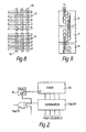
- the flat panel display 1 shown comprises a liquid crystal flat-panel 3 and electrode address drive circuitry 5.
- the panel electrodes are addressed using no more than two isogonal unipolar waveform address signals, W 1 , W 2 , simple antiphase square wave signals of common amplitude V i.e. one square wave signal and its inverse. These signals are generated using a pair of clocked shift-and-store bus registers 7 and 9. These also are arranged with their outputs connected to the row electrodes 11 and to the column electrodes 13. Signal inversion, and thus generation of the isogonal inverted signals, is controlled by means of two exclusive OR-gates 15 and 17, one connected to each register 7 and 9.
- a clock oscillator 19 is provided to clock both registers 7 and 9. This clock 19 is also connected to the strobe input ST, of each register 7 and 9, via a divide-down counter 21 and a monostable 23.
- the display also includes
- a flip-flop bistable 25 This is responsive to the monostable 23, and is connected to one input of each of the exclusive OR gates 15 and 17. The other input of each exclusive OR gate 15 and 17 is connected to a data comparator.
- One comparator 27 compares counter data with input Y-co-ordinate data.
- the other comparator, 29, compares the counter data with input X-co-ordinate data.
- the matrix comprises 16 rows and 16 columns.
- the circuit can be easily expanded to drive larger matrices.
- the shift registers 7 and 9 are fully loaded and the monostable 23, which is triggered from the negative going edge of the counter's final output, produces a strobe pulse which transfers "0"s from the column shift register 9 to all the column electrodes 3 and "I”s from the row shift register 7 to all the row electrodes 11.
- the flip-flop 25 is clocked, reversing the inputs to the shift registers.
- "I"s are fed to the column shift register 9 and "0"s to the row shift register 7.
- On the 32nd clock pulse "1"s are strobed out to the column electrodes 13, and "0"s to the row electrodes 11.
- the flip-flop 25 again changes state and the process repeats, resulting in square waves of opposite phase being applied to the column and row electrodes 13 and 11.
- the effect on the display is that the difference of the two waveforms W 1 and W 2 is applied across all the picture elements causing the whole display 1 to be maintained in the ON state.
- the electrode 13 to which this waveform is applied will have zero volts between it and all but one of the row electrodes, for identical signals are applied. This causes all but one of the picture elements, defined by this column electrode, to be held in the OFF state. Operation of the row register 7, row exclusive-OR gate 15 and row comparator 27 is exactly similar but for the position of the inverted level which is determined by Y-co-ordinate input data. As the X and Y co-ordinate input data is changed, the cross-wire feature 31 tracks across the display 3 to follow these changes. The cross-wire feature 31 is centred at all times on the co-ordinate positions defined by the input data.
- the two signals W 1 , W 2 used can be expressed as a string of binary digits:- For these two signals:- ie. each is of non-zero mean value; and, whereas a truly alternating voltage difference but, a non-zero RMS voltage.
- the signals W 1 , " 2 are thus isogonal, as defined.
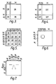
- FIGS. 3 - 7 Various waveform allocations are depicted in figures 3 - 7. These figures serve to illustrate some of the simple geometric symbols and features that can be achieved using isogonal signal drive.
- figures 3 - 5 only two isogonal drive signals W 1 and W 2 are required.
- W 1 and W 2 are required.
- both figures 3 and 5 which depict a cross-wire feature and a grid feature, respectively.
- most picture elements are driven ON.
- FIG 4 most picture elements are driven OFF.
- the ON state may correspond to either a transmissive or an opaque optical state.
- More complex patterned features or symbols may be obtained by the superposition of panels.
- a double panel comprised of three electrode-bearing plates, two electro-optic media and four sets of transparent electrodes, can be utilised.
- the two superimposed patterns may be of different colour, and like or reverse contrasts can be employed.
- one panel may be used as an attenuator or colour filter while the other is used to show the desired feature or symbol pattern.
- FIG 8 a concatenated electrode layout is shown, essentially a combination of sub-matrices.
- FIG 9 an interleaved electrode layout is shown. For simple depiction, only one representative column is shown.
- Concatenation or interleaving - as for example shown by figures 8 and 9 - may be used, either with single panels or with double panels, to increase the range of patterns which may be shown.
- a pair of features may be displayed by using odd rows and columns, for one, and even rows and columns for the other.
- a complex feature can then be formed by combination of two simpler features.
- the addressing technique disclosed above can be used to address an analogue meter having a variable pointer and an independently controlled additional pointer, e.g. a maximum or minimum limit stop.
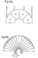
- One suitable electrode pattern is shown in Figures 10a, b.
- a front electrode pattern, Figure 10a has four sectors 41, 42, 43, 44 each with an addressing lead.
- a back electrode pattern, Figure 10b has four meander electrodes 45, 46, 47, 48 each having a section in register with each sector of the rear electrode.
- sixteen separately addressable pointers can be displayed.
- the addressing circuit can be arranged to give an audible warning when the set limit is exceeded.
- the additional pointer can be used to record the maximum or minimum deviation of the main pointer. If both a maximum and a minimum pointer are required they may be displayed alternately.
- a meter display is normally used in a reflective mode but could be used in a transmission mode.
- the electrode arrangement of Figure 10 is electrically equivalent to a four by four matrix as shown in Figures 11, where the front electrodes 41, 42, 43, 44 become row electrodes, and the back electrodes 45, 46, 47, 48 become column electrodes.
- waveforms W n is an integer, are applied to each electrode. n
- the allocation of waveforms are of four types:
- the flat panel aforementioned may be used as a dynamic or static overlay to printed, back-projected, and other static images. It may be used as a graticule in an optical sight, or in an imaging system or other similar optical system, for example a projection system.
- C.R.T. cathode ray tube
- OLED graticule an oscilloscope graticule
- the analogue meter display may be used in handheld and portable measurement instruments where low power consumption and low voltage operation are required.
Landscapes
- Engineering & Computer Science (AREA)
- Physics & Mathematics (AREA)
- Computer Hardware Design (AREA)
- General Physics & Mathematics (AREA)
- Theoretical Computer Science (AREA)
- Chemical & Material Sciences (AREA)
- Crystallography & Structural Chemistry (AREA)
- Control Of Indicators Other Than Cathode Ray Tubes (AREA)
- Liquid Crystal (AREA)
- Liquid Crystal Display Device Control (AREA)
- Indication In Cameras, And Counting Of Exposures (AREA)
Applications Claiming Priority (2)
| Application Number | Priority Date | Filing Date | Title |
|---|---|---|---|
| GB8408216 | 1984-03-30 | ||
| GB848408216A GB8408216D0 (en) | 1984-03-30 | 1984-03-30 | Flat-panel display |
Publications (2)
| Publication Number | Publication Date |
|---|---|
| EP0157524A2 true EP0157524A2 (fr) | 1985-10-09 |
| EP0157524A3 EP0157524A3 (fr) | 1987-04-01 |
Family
ID=10558912
Family Applications (1)
| Application Number | Title | Priority Date | Filing Date |
|---|---|---|---|
| EP85301823A Withdrawn EP0157524A3 (fr) | 1984-03-30 | 1985-03-15 | Panneau plat d'affichage |
Country Status (3)
| Country | Link |
|---|---|
| EP (1) | EP0157524A3 (fr) |
| JP (1) | JPS60222897A (fr) |
| GB (2) | GB8408216D0 (fr) |
Families Citing this family (3)
| Publication number | Priority date | Publication date | Assignee | Title |
|---|---|---|---|---|
| JPS6249399A (ja) * | 1985-08-29 | 1987-03-04 | キヤノン株式会社 | 表示装置 |
| SE466423B (sv) * | 1987-06-01 | 1992-02-10 | Gen Electric | Saett och anordning foer eliminering av oeverhoering vid matrisadresserade tunnfilmstranssistorbildenheter med flytande kristaller |
| US4873516A (en) * | 1987-06-01 | 1989-10-10 | General Electric Company | Method and system for eliminating cross-talk in thin film transistor matrix addressed liquid crystal displays |
Family Cites Families (10)
| Publication number | Priority date | Publication date | Assignee | Title |
|---|---|---|---|---|
| JPS5757718B2 (fr) * | 1973-10-19 | 1982-12-06 | Hitachi Ltd | |
| GB1463824A (en) * | 1974-02-13 | 1977-02-09 | Suncrux Research Office Kk | Liquid crystal display device |
| JPS5416894B2 (fr) * | 1974-03-01 | 1979-06-26 | ||
| GB1523162A (en) * | 1976-01-27 | 1978-08-31 | Secr Defence | Liquid crystal displays |
| GB1581221A (en) * | 1976-06-15 | 1980-12-10 | Citizen Watch Co Ltd | Matrix driving method for electro-optical display device |
| DE2644449C3 (de) * | 1976-10-01 | 1979-03-22 | Siemens Ag, 1000 Berlin Und 8000 Muenchen | Ansteuerverfahren für einen Anzeigeschirm mit einem zwischen den Zeilen und Spalten einer Leitermatrix befindlichen Medium, insbesondere einer Flüssigkristallschicht |
| GB2001794B (en) * | 1977-07-26 | 1982-01-27 | Secr Defence | Method of and apparatus for displaying waveforms |
| GB2044975B (en) * | 1979-01-26 | 1982-12-08 | Secr Defence | Pseudo-analogue display |
| GB2102178B (en) * | 1981-06-12 | 1985-03-27 | Interstate Electronics Corp | Plasma display panel control |
| EP0109160A3 (fr) * | 1982-10-14 | 1986-04-09 | The Secretary of State for Defence in Her Britannic Majesty's Government of the United Kingdom of Great Britain and | Dispositif d'affichage électronique |
-
1984
- 1984-03-30 GB GB848408216A patent/GB8408216D0/en active Pending
-
1985
- 1985-03-15 EP EP85301823A patent/EP0157524A3/fr not_active Withdrawn
- 1985-03-18 GB GB08506964A patent/GB2156567B/en not_active Expired
- 1985-03-28 JP JP6494085A patent/JPS60222897A/ja active Pending
Also Published As
| Publication number | Publication date |
|---|---|
| GB2156567A (en) | 1985-10-09 |
| EP0157524A3 (fr) | 1987-04-01 |
| JPS60222897A (ja) | 1985-11-07 |
| GB8506964D0 (en) | 1985-04-24 |
| GB8408216D0 (en) | 1984-05-10 |
| GB2156567B (en) | 1987-11-25 |
Similar Documents
| Publication | Publication Date | Title |
|---|---|---|
| US3982239A (en) | Saturation drive arrangements for optically bistable displays | |
| US4926168A (en) | Liquid crystal display device having a randomly determined polarity reversal frequency | |
| US4346378A (en) | Double trace electro optic display | |
| US4626840A (en) | Electronic display suitable for polar coordinate representations | |
| US3955187A (en) | Proportioning the address and data signals in a r.m.s. responsive display device matrix to obtain zero cross-talk and maximum contrast | |
| US4060801A (en) | Method and apparatus for non-scan matrix addressing of bar displays | |
| US4465999A (en) | Matrix driving method for electro-optical display device | |
| US4250503A (en) | Apparatus for displaying waveforms on a matrix display | |
| MY116641A (en) | Driving circuits for a passive matrix lcd which uses orthogonal functions to select different groups of scanning electrodes | |
| US3835463A (en) | Liquid crystal x{14 y matrix display device | |
| KR19980064172A (ko) | 광 변조 장치 | |
| CN1363081A (zh) | 多行寻址的显示装置 | |
| US4258364A (en) | Display device having adjoining display elements, and a method of producing the display device | |
| EP0157524A2 (fr) | Panneau plat d'affichage | |
| GB1592795A (en) | Data display screen systems utilising a bistable voltage-controlled medium | |
| US4429304A (en) | Display driving device | |
| US3987337A (en) | Plasma display panel having additional discharge cells of a larger effective area and driving circuit therefor | |
| GB1576498A (en) | Matrix driving method for electro-optical display device | |
| GB2065943A (en) | Controlling a digital display device of either dynamic or static type | |
| US4545649A (en) | Electro-optical display device of point matrix type | |
| JPS6157638B2 (fr) | ||
| GB2128387A (en) | Binary drive circuitry for matrix-addressed display | |
| JPH06167947A (ja) | 液晶素子等の駆動方法とその駆動回路及び表示装置 | |
| CN1386260A (zh) | 一种液晶显示设备和用一组扫描线的主动寻址和通过基于帧持续时间的非二进制划分的时间调制而得到的等级来驱动该液晶显示设备的方法 | |
| Ruckmongathan et al. | Sparse orthogonal matrices for scanning liquid crystal displays |
Legal Events
| Date | Code | Title | Description |
|---|---|---|---|
| PUAI | Public reference made under article 153(3) epc to a published international application that has entered the european phase |
Free format text: ORIGINAL CODE: 0009012 |
|
| AK | Designated contracting states |
Kind code of ref document: A2 Designated state(s): CH DE FR LI NL |
|
| PUAL | Search report despatched |
Free format text: ORIGINAL CODE: 0009013 |
|
| AK | Designated contracting states |
Kind code of ref document: A3 Designated state(s): CH DE FR LI NL |
|
| 17P | Request for examination filed |
Effective date: 19870512 |
|
| STAA | Information on the status of an ep patent application or granted ep patent |
Free format text: STATUS: THE APPLICATION HAS BEEN WITHDRAWN |
|
| 18W | Application withdrawn |
Withdrawal date: 19870914 |
|
| RIN1 | Information on inventor provided before grant (corrected) |
Inventor name: HUGHES, ANTHONY JAMES Inventor name: GLASPER, JOHN LEWIS Inventor name: CLARK, MICHAEL GEORGE Inventor name: SMITH, CHARLES JAMES THOMAS |