EP0157602A2 - Doppelheterostruktur-Halbleiterlaser für sichtbare Strahlung - Google Patents
Doppelheterostruktur-Halbleiterlaser für sichtbare Strahlung Download PDFInfo
- Publication number
- EP0157602A2 EP0157602A2 EP85302179A EP85302179A EP0157602A2 EP 0157602 A2 EP0157602 A2 EP 0157602A2 EP 85302179 A EP85302179 A EP 85302179A EP 85302179 A EP85302179 A EP 85302179A EP 0157602 A2 EP0157602 A2 EP 0157602A2
- Authority
- EP
- European Patent Office
- Prior art keywords
- layer
- ingaas
- semiconductor laser
- inalp
- ingasb
- Prior art date
- Legal status (The legal status is an assumption and is not a legal conclusion. Google has not performed a legal analysis and makes no representation as to the accuracy of the status listed.)
- Granted
Links
Images

Classifications
-
- H—ELECTRICITY
- H01—ELECTRIC ELEMENTS
- H01S—DEVICES USING THE PROCESS OF LIGHT AMPLIFICATION BY STIMULATED EMISSION OF RADIATION [LASER] TO AMPLIFY OR GENERATE LIGHT; DEVICES USING STIMULATED EMISSION OF ELECTROMAGNETIC RADIATION IN WAVE RANGES OTHER THAN OPTICAL
- H01S5/00—Semiconductor lasers
- H01S5/30—Structure or shape of the active region; Materials used for the active region
- H01S5/32—Structure or shape of the active region; Materials used for the active region comprising PN junctions, e.g. hetero- or double- heterostructures
- H01S5/323—Structure or shape of the active region; Materials used for the active region comprising PN junctions, e.g. hetero- or double- heterostructures in AIIIBV compounds, e.g. AlGaAs-laser, InP-based laser
- H01S5/32308—Structure or shape of the active region; Materials used for the active region comprising PN junctions, e.g. hetero- or double- heterostructures in AIIIBV compounds, e.g. AlGaAs-laser, InP-based laser emitting light at a wavelength less than 900 nm
- H01S5/32325—Structure or shape of the active region; Materials used for the active region comprising PN junctions, e.g. hetero- or double- heterostructures in AIIIBV compounds, e.g. AlGaAs-laser, InP-based laser emitting light at a wavelength less than 900 nm red laser based on InGaP
-
- H—ELECTRICITY
- H01—ELECTRIC ELEMENTS
- H01S—DEVICES USING THE PROCESS OF LIGHT AMPLIFICATION BY STIMULATED EMISSION OF RADIATION [LASER] TO AMPLIFY OR GENERATE LIGHT; DEVICES USING STIMULATED EMISSION OF ELECTROMAGNETIC RADIATION IN WAVE RANGES OTHER THAN OPTICAL
- H01S5/00—Semiconductor lasers
- H01S5/20—Structure or shape of the semiconductor body to guide the optical wave ; Confining structures perpendicular to the optical axis, e.g. index or gain guiding, stripe geometry, broad area lasers, gain tailoring, transverse or lateral reflectors, special cladding structures, MQW barrier reflection layers
- H01S5/24—Structure or shape of the semiconductor body to guide the optical wave ; Confining structures perpendicular to the optical axis, e.g. index or gain guiding, stripe geometry, broad area lasers, gain tailoring, transverse or lateral reflectors, special cladding structures, MQW barrier reflection layers having a grooved structure, e.g. V-grooved, crescent active layer in groove, VSIS laser
-
- H—ELECTRICITY
- H01—ELECTRIC ELEMENTS
- H01S—DEVICES USING THE PROCESS OF LIGHT AMPLIFICATION BY STIMULATED EMISSION OF RADIATION [LASER] TO AMPLIFY OR GENERATE LIGHT; DEVICES USING STIMULATED EMISSION OF ELECTROMAGNETIC RADIATION IN WAVE RANGES OTHER THAN OPTICAL
- H01S5/00—Semiconductor lasers
- H01S5/02—Structural details or components not essential to laser action
- H01S5/0206—Substrates, e.g. growth, shape, material, removal or bonding
Definitions
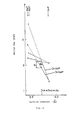
- the energy difference therebetween can be maintained at a high level, while crystal defects result from the non-coincidence between the lattice constants so that the threshold current increases and/or the lifetime is reduced.
Landscapes
- Physics & Mathematics (AREA)
- Condensed Matter Physics & Semiconductors (AREA)
- General Physics & Mathematics (AREA)
- Electromagnetism (AREA)
- Optics & Photonics (AREA)
- Geometry (AREA)
- Semiconductor Lasers (AREA)
Applications Claiming Priority (2)
| Application Number | Priority Date | Filing Date | Title |
|---|---|---|---|
| JP59062287A JPS60206081A (ja) | 1984-03-29 | 1984-03-29 | 半導体レ−ザ装置 |
| JP62287/84 | 1984-03-29 |
Publications (3)
| Publication Number | Publication Date |
|---|---|
| EP0157602A2 true EP0157602A2 (de) | 1985-10-09 |
| EP0157602A3 EP0157602A3 (en) | 1987-06-03 |
| EP0157602B1 EP0157602B1 (de) | 1991-01-16 |
Family
ID=13195750
Family Applications (1)
| Application Number | Title | Priority Date | Filing Date |
|---|---|---|---|
| EP85302179A Expired EP0157602B1 (de) | 1984-03-29 | 1985-03-28 | Doppelheterostruktur-Halbleiterlaser für sichtbare Strahlung |
Country Status (4)
| Country | Link |
|---|---|
| US (1) | US4712219A (de) |
| EP (1) | EP0157602B1 (de) |
| JP (1) | JPS60206081A (de) |
| DE (1) | DE3581304D1 (de) |
Cited By (2)
| Publication number | Priority date | Publication date | Assignee | Title |
|---|---|---|---|---|
| FR2703188A1 (fr) * | 1993-03-23 | 1994-09-30 | Fujitsu Ltd | Dispositif à semiconducteur optique doté d'un puits quantique contraint. |
| EP2628183A4 (de) * | 2010-10-12 | 2014-04-02 | Alliance Sustainable Energy | Gruppe-iii-v-legierungen mit hoher bandlücke für hocheffiziente optoelektronik |
Families Citing this family (12)
| Publication number | Priority date | Publication date | Assignee | Title |
|---|---|---|---|---|
| JPS63299186A (ja) * | 1987-05-29 | 1988-12-06 | Hitachi Ltd | 発光素子 |
| US4829343A (en) * | 1987-07-17 | 1989-05-09 | American Telephone & Telegraph Company, At&T Bell Laboratories | Hot electron transistor |
| US5146295A (en) * | 1988-03-29 | 1992-09-08 | Omron Tateisi Electronic Co. | Semiconductor light emitting device having a superlattice buffer layer |
| US5048036A (en) * | 1989-09-18 | 1991-09-10 | Spectra Diode Laboratories, Inc. | Heterostructure laser with lattice mismatch |
| US4984242A (en) * | 1989-09-18 | 1991-01-08 | Spectra Diode Laboratories, Inc. | GaAs/AlGaAs heterostructure laser containing indium |
| US5200972A (en) * | 1991-06-17 | 1993-04-06 | The United States Of America As Represented By The Secretary Of The Navy | ND laser with co-doped ion(s) pumped by visible laser diodes |
| JPH07183618A (ja) * | 1993-12-22 | 1995-07-21 | Ricoh Co Ltd | 半導体レーザ装置、半導体レーザ装置製造方法並びに集積型半導体レーザ装置 |
| US5550065A (en) * | 1994-11-25 | 1996-08-27 | Motorola | Method of fabricating self-aligned FET structure having a high temperature stable T-shaped Schottky gate contact |
| US5751753A (en) * | 1995-07-24 | 1998-05-12 | Fujitsu Limited | Semiconductor laser with lattice mismatch |
| US6181721B1 (en) * | 1996-05-20 | 2001-01-30 | Sdl, Inc. | Visible wavelength, semiconductor optoelectronic device with a high power broad, significantly laterally uniform, diffraction limited output beam |
| US5838705A (en) * | 1996-11-04 | 1998-11-17 | Motorola, Inc. | Light emitting device having a defect inhibition layer |
| CN102037575B (zh) * | 2008-03-27 | 2013-04-10 | 宋俊午 | 发光元件及其制造方法 |
Family Cites Families (5)
| Publication number | Priority date | Publication date | Assignee | Title |
|---|---|---|---|---|
| JPS542829B2 (de) * | 1973-02-26 | 1979-02-14 | ||
| JPS5320881A (en) * | 1976-08-11 | 1978-02-25 | Nippon Telegr & Teleph Corp <Ntt> | Photo semiconductor device |
| JPS5640292A (en) * | 1979-09-11 | 1981-04-16 | Fujitsu Ltd | Semiconductor laser |
| JPS5727095A (en) * | 1980-07-25 | 1982-02-13 | Toshiba Corp | Semiconductor light emitting device |
| FR2508244A1 (fr) * | 1981-06-19 | 1982-12-24 | Thomson Csf | Laser a semi-conducteur a courte longueur d'onde |
-
1984
- 1984-03-29 JP JP59062287A patent/JPS60206081A/ja active Pending
-
1985
- 1985-03-26 US US06/716,222 patent/US4712219A/en not_active Expired - Fee Related
- 1985-03-28 EP EP85302179A patent/EP0157602B1/de not_active Expired
- 1985-03-28 DE DE8585302179T patent/DE3581304D1/de not_active Expired - Lifetime
Cited By (3)
| Publication number | Priority date | Publication date | Assignee | Title |
|---|---|---|---|---|
| FR2703188A1 (fr) * | 1993-03-23 | 1994-09-30 | Fujitsu Ltd | Dispositif à semiconducteur optique doté d'un puits quantique contraint. |
| US5841152A (en) * | 1993-03-23 | 1998-11-24 | Fujitsu Limited | Optical semiconductor device provided with strained quantum well layer formed on a ternary compound semiconductor substrate |
| EP2628183A4 (de) * | 2010-10-12 | 2014-04-02 | Alliance Sustainable Energy | Gruppe-iii-v-legierungen mit hoher bandlücke für hocheffiziente optoelektronik |
Also Published As
| Publication number | Publication date |
|---|---|
| JPS60206081A (ja) | 1985-10-17 |
| EP0157602A3 (en) | 1987-06-03 |
| US4712219A (en) | 1987-12-08 |
| DE3581304D1 (de) | 1991-02-21 |
| EP0157602B1 (de) | 1991-01-16 |
Similar Documents
| Publication | Publication Date | Title |
|---|---|---|
| EP0157602B1 (de) | Doppelheterostruktur-Halbleiterlaser für sichtbare Strahlung | |
| US4941146A (en) | Semiconductor laser device | |
| US5038185A (en) | Structurally consistent surface skimming hetero-transverse junction lasers and lateral heterojunction bipolar transistors | |
| US4734385A (en) | Semiconductor laser element suitable for production by a MO-CVD method | |
| US6072817A (en) | Semiconductor laser device and optical disk apparatus using the same | |
| US4982409A (en) | Semiconductor laser device | |
| US6118800A (en) | Semiconductor laser and cleaving method | |
| US5375136A (en) | Semiconductor laser of patterned-substrate type and structure thereof | |
| US4121179A (en) | Semiconductor injection laser | |
| US4674094A (en) | Semiconductor laser with an active layer having varying thicknesses | |
| US5360762A (en) | Semiconductor laser device, and a method for producing a compound semiconductor device including the semiconductor laser device | |
| US5337326A (en) | Semiconductor laser device with compressively stressed barrier layer | |
| US5291506A (en) | Semiconductor laser made of group II-VI compounds | |
| US6055255A (en) | Semiconductor laser device and method for producing the same | |
| KR100590565B1 (ko) | 반도체 레이저 다이오드 및 그 제조 방법 | |
| EP0289308B1 (de) | Halbleiterlaservorrichtung | |
| US5289487A (en) | Semiconductor laser device having uniform and reproducible laser characteristics | |
| EP0915542A2 (de) | Halbleiterlaser mit verbesserten stromsperrenden Schichten und Herstellungsverfahren | |
| EP0306314B1 (de) | Halbleiterlaser-Vorrichtung | |
| US5151912A (en) | Semiconductor laser | |
| JPH07109924B2 (ja) | 半導体レーザ装置及びその製造方法 | |
| KR100261243B1 (ko) | 레이저 다이오드 및 그의 제조방법 | |
| JP2891756B2 (ja) | 波長可変半導体レーザ | |
| KR0179017B1 (ko) | 레이저 다이오드의 제조방법 | |
| KR100408526B1 (ko) | GaN계레이저다이오드 |
Legal Events
| Date | Code | Title | Description |
|---|---|---|---|
| PUAI | Public reference made under article 153(3) epc to a published international application that has entered the european phase |
Free format text: ORIGINAL CODE: 0009012 |
|
| AK | Designated contracting states |
Designated state(s): DE GB NL |
|
| 17P | Request for examination filed |
Effective date: 19861223 |
|
| PUAL | Search report despatched |
Free format text: ORIGINAL CODE: 0009013 |
|
| AK | Designated contracting states |
Kind code of ref document: A3 Designated state(s): DE GB NL |
|
| 17Q | First examination report despatched |
Effective date: 19891113 |
|
| GRAA | (expected) grant |
Free format text: ORIGINAL CODE: 0009210 |
|
| AK | Designated contracting states |
Kind code of ref document: B1 Designated state(s): DE GB NL |
|
| REF | Corresponds to: |
Ref document number: 3581304 Country of ref document: DE Date of ref document: 19910221 |
|
| PLBE | No opposition filed within time limit |
Free format text: ORIGINAL CODE: 0009261 |
|
| STAA | Information on the status of an ep patent application or granted ep patent |
Free format text: STATUS: NO OPPOSITION FILED WITHIN TIME LIMIT |
|
| 26N | No opposition filed | ||
| PGFP | Annual fee paid to national office [announced via postgrant information from national office to epo] |
Ref country code: GB Payment date: 19980319 Year of fee payment: 14 |
|
| PGFP | Annual fee paid to national office [announced via postgrant information from national office to epo] |
Ref country code: NL Payment date: 19980326 Year of fee payment: 14 |
|
| PGFP | Annual fee paid to national office [announced via postgrant information from national office to epo] |
Ref country code: DE Payment date: 19980403 Year of fee payment: 14 |
|
| PG25 | Lapsed in a contracting state [announced via postgrant information from national office to epo] |
Ref country code: GB Free format text: LAPSE BECAUSE OF NON-PAYMENT OF DUE FEES Effective date: 19990328 |
|
| PG25 | Lapsed in a contracting state [announced via postgrant information from national office to epo] |
Ref country code: NL Free format text: LAPSE BECAUSE OF NON-PAYMENT OF DUE FEES Effective date: 19991001 |
|
| GBPC | Gb: european patent ceased through non-payment of renewal fee |
Effective date: 19990328 |
|
| NLV4 | Nl: lapsed or anulled due to non-payment of the annual fee |
Effective date: 19991001 |
|
| PG25 | Lapsed in a contracting state [announced via postgrant information from national office to epo] |
Ref country code: DE Free format text: LAPSE BECAUSE OF NON-PAYMENT OF DUE FEES Effective date: 20000101 |