EP0157607A2 - Système d'emmagasinage de données analogiques - Google Patents
Système d'emmagasinage de données analogiques Download PDFInfo
- Publication number
- EP0157607A2 EP0157607A2 EP85302197A EP85302197A EP0157607A2 EP 0157607 A2 EP0157607 A2 EP 0157607A2 EP 85302197 A EP85302197 A EP 85302197A EP 85302197 A EP85302197 A EP 85302197A EP 0157607 A2 EP0157607 A2 EP 0157607A2
- Authority
- EP
- European Patent Office
- Prior art keywords
- column
- array
- row
- cell
- rows
- Prior art date
- Legal status (The legal status is an assumption and is not a legal conclusion. Google has not performed a legal analysis and makes no representation as to the accuracy of the status listed.)
- Granted
Links
Images


Classifications
-
- G—PHYSICS
- G11—INFORMATION STORAGE
- G11C—STATIC STORES
- G11C27/00—Electric analogue stores, e.g. for storing instantaneous values
- G11C27/04—Shift registers
-
- G—PHYSICS
- G11—INFORMATION STORAGE
- G11C—STATIC STORES
- G11C27/00—Electric analogue stores, e.g. for storing instantaneous values
- G11C27/02—Sample-and-hold arrangements
- G11C27/024—Sample-and-hold arrangements using a capacitive memory element
- G11C27/026—Sample-and-hold arrangements using a capacitive memory element associated with an amplifier
Definitions
- the invention is directed generally to an analog data storage system and -more particularly to such a system for very high speed sampling of analog pulse information, the pulse widths being in the range of 10s of nanoseconds.
- An increasingly important problem in large scale physics detectors is the sampling of and recording of analog pulse information for-pulse widths in the range of a few tens of nanoseconds with accuracy of the order of one percent and with a dynamic range of the order of eleven bits (one part in two-thousand).
- the generation of high precision time and amplitude information related to the outputs from various kinds of detectors is of considerable significance in applications including high energy physics, transient digitizing of signals associated with nuclear impulses, laser fusion, optic communication, and general lab measurement methods. In most known systems, the accuracy degrades significantly as the signal to be sampled approaches the low end of the dynamic range. It is therefore an object of the present invention to provide an analog pulse sampling system and method which can maintain a high level of accuracy over a wide dynamic range.
- An objective of the present invention is to provide an improved analog pulse storage integrated circuit.
- An objective of the present invention is to provide an integrated detector which is of small size, low power, and low cost to be used to detect the signal values carried on each channel.
- an effective sampling rate of 2 x 10 8 samples per second is desirable, while maintaining accuracy on the order of 11 bits.
- An objective of the present invention is to provide analog pulse sampling information comprising a plurality of sample points for a pulse on any given channel, each sample -having an aperture of about 1 nanosecond with a sample time position error less than or equal to 0.1 nanosecond.
- the sample clock interval should be both very regular and at extremely high frequency to provide a maximum number of samples across the pulse, which may have a pulse width of no more than a few 10's of nanoseconds.
- Another objective of the present invention is to provide an integrated circuit solution, in order to reduce the cost and maximize the speed of the sampling chip. It is therefore highly desirable to provide a chip having a sampling cell design which is highly regular and thus extremely reproducible on a large scale.
- a second known prior art device is the RETICON 5501 which is a bucket brigade device of-a well known design.
- this device as with the device described above must be cascaded, so that it suffers from drive problems and size limitation. Also, because of the way the circuit is designed, the sampling rate cannot b'e controlled except by cable delay of the sampling gate which is very cumbersome. The sampling aperture time is relatively limited.
- the analog storage system described in IEEE Transactions on Nuclear Science, Vol NS30, February 1983 at page 339-341 suffers from the same limitations, due to the use of a delay line.
- Another method in some general use is to place a high speed or flash ADC analog to digital converter on each channel.
- Such devices work at rates of 100 x 10 samples per second (100 mhz) but yield accuracies no better than 5 to 6 bits, unless extended by elaborate additional circuitry.
- the cost of a single converter and the power consumption for each converter are both undesirably high for large systems, and probably impractical for systems for greater than 100,000 channels.
- each storage cell is defined to include two input gates between the pulse input at which the analog pulse information is received, and a storage capacitor for storing the analog signal level for the defined aperture.
- the cells are arrayed in rows and columns, and the input gates are controlled by separate row and column clocks.
- One of the clocks operates at a relatively low rate; the other clock operates at the rate of sampling. Data is read and stored by each cell only on coincidence of the two clocks. Therefore, if the low speed clock is the column clock, and the high speed clock is the row clock, then the column clock need shift from column to column only after every row cell in that column has been activated by the row clock.
- one clock may be continuously running, the other clock being initiated by detection of the pulse to be sampled, or by receipt of a known time marker or trigger synchronously with the arrival of the data pulse to be sampled.
- the storage time can be extended to any length compatible with the ultimate data storage device.
- a separate reference cell is provided of identical design to all of the storage cells on the chip, but not receiving any of the analog pulse information.
- the columns are divided vertically into two halves. Therefore, the column pulse which activates the controls for the cells in the bottom half of the column can overlap in real time with the pulse being used to activate the control gates for the other half of the column.
- the speed of the actual pulse writing (storage) is.optimized, while minimizing the complexity of the input clock timing circuitry.
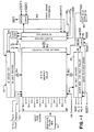
- the basic elements of the analog storage integrated circuit are shown in figure 1. All These elements illustrated are on chip except the row gate pulse generator 12 which comprises the row clock trigger.
- a differential buffer (not shown) is also provided for reading out the stored data to a remote memory.
- the input signal which is an analog pulse typically of a few 10's of nanoseconds is applied simultaneously to all of the inputs of all'of the cells via inputs SIG1 and SIG2.
- Each cell is designed in accordance with the schematic shown in figure 3.
- each of the cells includes a storage capacitor 20 which is capable of storing charge only during the time period that both of the input gate transistors Ql, Q2 are turned on. The other details of the cell of Figure 3 are explained below.
- the row gate clock pulse generator 1 . 2 runs continuously at the analog pulse sampling rate.
- the arrival of the analog data pulse on input lines SIG1, SIG2 is signaled by either a threshold detector which detects the actual pulse, or a pulse detector which receives a trigger pulse which is transmitted in timed relation to receipt of the analog pulse.
- Turning on the column counter 28 will now transmit column clock input signals to each of the memory cells in turn. This signal to each cell is shown as 0c at gate Q2 in Figure 3.
- Coincidence of the row and column clock signals at any gate allows storage of a brief analog sample (aperture about 1 nanosecond) of the data pulse on the storage capacitor. Signal storage occurs when 0 ⁇ f makes a high to low transition, turning OFF Ql.
- the stored value cannot be altered by 0 ⁇ f being at a high state if 0 is low so that Q2 is off.
- the gate transi s- tors are separately activated by a row clock generator 12 and a column gate pulse generator 28 which includes a unit driver 29 and shift register 30.
- a row clock generator 12 and a column gate pulse generator 28 which includes a unit driver 29 and shift register 30.
- the 16 fast clock pulses are provided to rows which are interleaved; that is, the numbers on the 16 inputs represent the order in which the rows are triggered. This is to allow for the propagation time of the column clock signals up the columns, since the row clock signals are transferred horizontally on metal lines which carry signals at very fast speeds, but the clock signals run vertically up polysilicon lines which have longer propagation delays.
- each column is actually divided in two sections. That is, in each vertical column of 16 cells, 8 of the cells are triggered by one output of the shift register and driver 28. The other 8 cells, are triggered off a second output. Thus for example alternate groups of cells in the trigger sequence (1-8,9-16) are triggered by alternate column clock outputs (0 ⁇ c1,0 ⁇ c2).
- the input shift register 28 which provides column clock signals to the columns has 32 outputs (0 ⁇ c1,...0 ⁇ c32).
- the input shift register 28 (shown in figure 2) comprises a set of half-shift registers 30 and accompanying drivers, both of standard design. The major control signals which are used to implement this timed storage operation are shown both in figure 2 and figure 1;
- INHS runs to column access drivers; if low, turns off the column clocks so no cells can be turned on, preventing an attempt to store data into a cell which has not yet been read of previously stored data.
- RESET initializes all registers to starting state.
- START puts bit in first register to be advanced through registers by 0 ⁇ 1s, 02s.
- INHRI if low, clears all column clocks to 0; if high, then recirculation occurs, so that the first two half shift registers are high, (see Figure 2) and the rest are zero.
- the Recirculation logic, 35 shown in detail in Figure 2, responds to and generates these last three signals. Generation of the other identified signals is accomplished by techniques well known in this art.
- the x and y coordinate output shift registers 32, 34 are of similar design to those shown in Figure 2.
- the clock logic is used to simplify chip layout, as these shift registers run at the same rate-typically significantly slower than the input rate.
- each cell includes in addition to the input section a highly linear output stage.
- each memory cell includes a nonloading readout amplifier section 40, and multiplex readout portion 42 for conveying a linear representation of the charge stored on the capacitor 20 through the multiplex readout portions 42 and 44 to the chip outputs OUT and OUT.
- Each of the output sections including the non-loading amplifier 40 and the buffer amplifier 42 comprise matched pairs of identical transistors.
- the input to the transistor Q5 of amplifier 40 is connected to the capacitor C s .
- a linear representation of the magnitude of the voltage stored on the capacitor 20 can be applied to the output bus through the multiplexor 44.
- a reference cell 60 shown in detail in figure 4 is provided on each chip.
- the design of the reference cell 60 is identical to the design of each of the memory cells in the array.
- the cell is pulsed by INHS after all data cells have received the data which they are to store; thus the voltage V ref which is applied to the transistor Q6 provides a differential reference level which is coupled through transistors Q8, Q10, Q12, and Q14 to the output bus so that a reference level is always available which accounts for the temperature changes and capacitor leakage.
- the output being read as a differential output will accurately represent the analog pulse sample.
- the use of differential signal readout for Vsig, together with careful use of matched transistor pairs 40 and 42 from C and V ref through the multiplexer 44 to the output prevents signal level errors due to process and temperature variations.
- a signal 0reset is provided to gate a transistor Q4 connected across the storage capacitor 20 incorporated in each memory cell. This is provided to allow for draining the storage capacitor 20 to ground after the data has been read out to remote storage.
- a second signal (6INH is provided to gate a transistor Q3 connected to a node in between the two gate transistors Ql, Q2. This is used to ground the intermediate node, so that any leakage current, gate or signal feed-through from the first gate, which is the gate receiving the continuously running fast row clock pulses, does not affect the readout of the storage capacitor 20.
- the integrated circuit design of the present invention provides a number of significant advantages in the field of physics data recording.
- the use of NMOS IC technology, for the analog storage cell allows an order of magnitude improvement in density and makes practical systems of a very large scale because of the ease of reproduction of the integrated circuit and the low power consumption.
- the accuracy of the analog samples recorded will be significantly improved because of the identity of every cell. in the memory cell array.
- the power consumption will be significantly reduced over known prior art methods such as Flash A/D converters. Any high power circuitry required for drive purposes can be shared by many channels.
- the dynamic range, the sampling aperture, and the accuracy are much improved over known methods.
Landscapes
- Analogue/Digital Conversion (AREA)
- Measurement Of Current Or Voltage (AREA)
- Networks Using Active Elements (AREA)
Applications Claiming Priority (2)
| Application Number | Priority Date | Filing Date | Title |
|---|---|---|---|
| US59579084A | 1984-04-02 | 1984-04-02 | |
| US595790 | 1984-04-02 |
Publications (3)
| Publication Number | Publication Date |
|---|---|
| EP0157607A2 true EP0157607A2 (fr) | 1985-10-09 |
| EP0157607A3 EP0157607A3 (en) | 1988-01-20 |
| EP0157607B1 EP0157607B1 (fr) | 1993-02-10 |
Family
ID=24384687
Family Applications (1)
| Application Number | Title | Priority Date | Filing Date |
|---|---|---|---|
| EP85302197A Expired - Lifetime EP0157607B1 (fr) | 1984-04-02 | 1985-03-29 | Système d'emmagasinage de données analogiques |
Country Status (6)
| Country | Link |
|---|---|
| US (1) | US4811285A (fr) |
| EP (1) | EP0157607B1 (fr) |
| JP (1) | JPS615499A (fr) |
| AU (1) | AU579856B2 (fr) |
| CA (1) | CA1230421A (fr) |
| DE (1) | DE3587082T2 (fr) |
Cited By (4)
| Publication number | Priority date | Publication date | Assignee | Title |
|---|---|---|---|---|
| EP0322074A3 (en) * | 1987-12-23 | 1989-10-18 | Philips Electronic And Associated Industries Limited | Circuit arrangement for processing sampled analogue electrical signals |
| EP0440653A4 (en) * | 1988-07-13 | 1991-10-16 | Information Storage Devices, Inc. | High density integrated circuit analog signal recording and playback system |
| EP0317236B1 (fr) * | 1987-11-16 | 1994-02-16 | Tektronix, Inc. | Système d'acquisition de données |
| EP0741391B1 (fr) * | 1990-01-26 | 2000-02-23 | Kabushiki Kaisha Toshiba | Circuit échantillonneur et de maintien |
Families Citing this family (81)
| Publication number | Priority date | Publication date | Assignee | Title |
|---|---|---|---|---|
| US5241494A (en) * | 1990-09-26 | 1993-08-31 | Information Storage Devices | Integrated circuit system for analog signal recording and playback |
| US5243469A (en) * | 1990-11-14 | 1993-09-07 | Union Oil Company Of California | System for the acquisition of seismic data |
| US6222762B1 (en) * | 1992-01-14 | 2001-04-24 | Sandisk Corporation | Multi-state memory |
| US5712180A (en) * | 1992-01-14 | 1998-01-27 | Sundisk Corporation | EEPROM with split gate source side injection |
| US5313421A (en) * | 1992-01-14 | 1994-05-17 | Sundisk Corporation | EEPROM with split gate source side injection |
| US7071060B1 (en) | 1996-02-28 | 2006-07-04 | Sandisk Corporation | EEPROM with split gate source side infection with sidewall spacers |
| US5400343A (en) * | 1992-02-28 | 1995-03-21 | Intel Corporation | Apparatus and method for defective column detection for semiconductor memories |
| US5359896A (en) * | 1992-09-03 | 1994-11-01 | The United States Of America As Represented By The Administrator Of The National Aeronautics And Space Administration | Acceleration recorder and playback module |
| US5504699A (en) * | 1994-04-08 | 1996-04-02 | Goller; Stuart E. | Nonvolatile magnetic analog memory |
| KR100272472B1 (ko) * | 1995-09-19 | 2000-11-15 | 씨. 필립 채프맨 | 디지탈 프로그램가능 임계 레벨을 가진 마이크로컨트롤러 재작동 기능 |
| KR100299564B1 (ko) * | 1997-12-31 | 2001-10-27 | 박종섭 | 펄스드라이버 |
| FR2824177B1 (fr) * | 2001-04-26 | 2004-12-03 | Centre Nat Rech Scient | Echantillonneur analogique rapide a grande profondeur memoire |
| JP2005530460A (ja) * | 2002-06-20 | 2005-10-06 | ダコタ・テクノロジーズ・インコーポレーテッド | 過渡信号をデジタル化するシステム |
| US6975251B2 (en) * | 2002-06-20 | 2005-12-13 | Dakota Technologies, Inc. | System for digitizing transient signals with waveform accumulator |
| US8156403B2 (en) * | 2006-05-12 | 2012-04-10 | Anobit Technologies Ltd. | Combined distortion estimation and error correction coding for memory devices |
| CN103280239B (zh) * | 2006-05-12 | 2016-04-06 | 苹果公司 | 存储设备中的失真估计和消除 |
| US7697326B2 (en) | 2006-05-12 | 2010-04-13 | Anobit Technologies Ltd. | Reducing programming error in memory devices |
| US8239735B2 (en) * | 2006-05-12 | 2012-08-07 | Apple Inc. | Memory Device with adaptive capacity |
| US8060806B2 (en) | 2006-08-27 | 2011-11-15 | Anobit Technologies Ltd. | Estimation of non-linear distortion in memory devices |
| US7821826B2 (en) | 2006-10-30 | 2010-10-26 | Anobit Technologies, Ltd. | Memory cell readout using successive approximation |
| US7975192B2 (en) * | 2006-10-30 | 2011-07-05 | Anobit Technologies Ltd. | Reading memory cells using multiple thresholds |
| US7924648B2 (en) | 2006-11-28 | 2011-04-12 | Anobit Technologies Ltd. | Memory power and performance management |
| WO2008068747A2 (fr) | 2006-12-03 | 2008-06-12 | Anobit Technologies Ltd. | Gestion automatique de défauts dans des dispositifs à mémoire |
| US7593263B2 (en) * | 2006-12-17 | 2009-09-22 | Anobit Technologies Ltd. | Memory device with reduced reading latency |
| US7900102B2 (en) * | 2006-12-17 | 2011-03-01 | Anobit Technologies Ltd. | High-speed programming of memory devices |
| US7751240B2 (en) * | 2007-01-24 | 2010-07-06 | Anobit Technologies Ltd. | Memory device with negative thresholds |
| US8151166B2 (en) * | 2007-01-24 | 2012-04-03 | Anobit Technologies Ltd. | Reduction of back pattern dependency effects in memory devices |
| WO2008111058A2 (fr) * | 2007-03-12 | 2008-09-18 | Anobit Technologies Ltd. | Estimation adaptative de seuils de lecture de cellules mémoires |
| US8001320B2 (en) * | 2007-04-22 | 2011-08-16 | Anobit Technologies Ltd. | Command interface for memory devices |
| US8429493B2 (en) | 2007-05-12 | 2013-04-23 | Apple Inc. | Memory device with internal signap processing unit |
| US8234545B2 (en) * | 2007-05-12 | 2012-07-31 | Apple Inc. | Data storage with incremental redundancy |
| US7925936B1 (en) | 2007-07-13 | 2011-04-12 | Anobit Technologies Ltd. | Memory device with non-uniform programming levels |
| US8259497B2 (en) | 2007-08-06 | 2012-09-04 | Apple Inc. | Programming schemes for multi-level analog memory cells |
| US8174905B2 (en) * | 2007-09-19 | 2012-05-08 | Anobit Technologies Ltd. | Programming orders for reducing distortion in arrays of multi-level analog memory cells |
| US7773413B2 (en) | 2007-10-08 | 2010-08-10 | Anobit Technologies Ltd. | Reliable data storage in analog memory cells in the presence of temperature variations |
| US8068360B2 (en) * | 2007-10-19 | 2011-11-29 | Anobit Technologies Ltd. | Reading analog memory cells using built-in multi-threshold commands |
| US8000141B1 (en) | 2007-10-19 | 2011-08-16 | Anobit Technologies Ltd. | Compensation for voltage drifts in analog memory cells |
| US8527819B2 (en) * | 2007-10-19 | 2013-09-03 | Apple Inc. | Data storage in analog memory cell arrays having erase failures |
| KR101509836B1 (ko) * | 2007-11-13 | 2015-04-06 | 애플 인크. | 멀티 유닛 메모리 디바이스에서의 메모리 유닛의 최적화된 선택 |
| US8225181B2 (en) | 2007-11-30 | 2012-07-17 | Apple Inc. | Efficient re-read operations from memory devices |
| US8209588B2 (en) * | 2007-12-12 | 2012-06-26 | Anobit Technologies Ltd. | Efficient interference cancellation in analog memory cell arrays |
| US8456905B2 (en) | 2007-12-16 | 2013-06-04 | Apple Inc. | Efficient data storage in multi-plane memory devices |
| US8085586B2 (en) * | 2007-12-27 | 2011-12-27 | Anobit Technologies Ltd. | Wear level estimation in analog memory cells |
| US8156398B2 (en) * | 2008-02-05 | 2012-04-10 | Anobit Technologies Ltd. | Parameter estimation based on error correction code parity check equations |
| US7924587B2 (en) * | 2008-02-21 | 2011-04-12 | Anobit Technologies Ltd. | Programming of analog memory cells using a single programming pulse per state transition |
| US7864573B2 (en) | 2008-02-24 | 2011-01-04 | Anobit Technologies Ltd. | Programming analog memory cells for reduced variance after retention |
| US8230300B2 (en) * | 2008-03-07 | 2012-07-24 | Apple Inc. | Efficient readout from analog memory cells using data compression |
| US8059457B2 (en) * | 2008-03-18 | 2011-11-15 | Anobit Technologies Ltd. | Memory device with multiple-accuracy read commands |
| US8400858B2 (en) | 2008-03-18 | 2013-03-19 | Apple Inc. | Memory device with reduced sense time readout |
| US7995388B1 (en) | 2008-08-05 | 2011-08-09 | Anobit Technologies Ltd. | Data storage using modified voltages |
| US7924613B1 (en) * | 2008-08-05 | 2011-04-12 | Anobit Technologies Ltd. | Data storage in analog memory cells with protection against programming interruption |
| US8169825B1 (en) | 2008-09-02 | 2012-05-01 | Anobit Technologies Ltd. | Reliable data storage in analog memory cells subjected to long retention periods |
| US8949684B1 (en) | 2008-09-02 | 2015-02-03 | Apple Inc. | Segmented data storage |
| US8482978B1 (en) | 2008-09-14 | 2013-07-09 | Apple Inc. | Estimation of memory cell read thresholds by sampling inside programming level distribution intervals |
| US8000135B1 (en) | 2008-09-14 | 2011-08-16 | Anobit Technologies Ltd. | Estimation of memory cell read thresholds by sampling inside programming level distribution intervals |
| US8239734B1 (en) | 2008-10-15 | 2012-08-07 | Apple Inc. | Efficient data storage in storage device arrays |
| US8261159B1 (en) | 2008-10-30 | 2012-09-04 | Apple, Inc. | Data scrambling schemes for memory devices |
| US8208304B2 (en) * | 2008-11-16 | 2012-06-26 | Anobit Technologies Ltd. | Storage at M bits/cell density in N bits/cell analog memory cell devices, M>N |
| US8174857B1 (en) | 2008-12-31 | 2012-05-08 | Anobit Technologies Ltd. | Efficient readout schemes for analog memory cell devices using multiple read threshold sets |
| US8248831B2 (en) * | 2008-12-31 | 2012-08-21 | Apple Inc. | Rejuvenation of analog memory cells |
| US8924661B1 (en) | 2009-01-18 | 2014-12-30 | Apple Inc. | Memory system including a controller and processors associated with memory devices |
| US8228701B2 (en) | 2009-03-01 | 2012-07-24 | Apple Inc. | Selective activation of programming schemes in analog memory cell arrays |
| US8832354B2 (en) * | 2009-03-25 | 2014-09-09 | Apple Inc. | Use of host system resources by memory controller |
| US8259506B1 (en) | 2009-03-25 | 2012-09-04 | Apple Inc. | Database of memory read thresholds |
| US8238157B1 (en) | 2009-04-12 | 2012-08-07 | Apple Inc. | Selective re-programming of analog memory cells |
| US8479080B1 (en) | 2009-07-12 | 2013-07-02 | Apple Inc. | Adaptive over-provisioning in memory systems |
| US8495465B1 (en) | 2009-10-15 | 2013-07-23 | Apple Inc. | Error correction coding over multiple memory pages |
| US8677054B1 (en) | 2009-12-16 | 2014-03-18 | Apple Inc. | Memory management schemes for non-volatile memory devices |
| US8694814B1 (en) | 2010-01-10 | 2014-04-08 | Apple Inc. | Reuse of host hibernation storage space by memory controller |
| US8572311B1 (en) | 2010-01-11 | 2013-10-29 | Apple Inc. | Redundant data storage in multi-die memory systems |
| US8694853B1 (en) | 2010-05-04 | 2014-04-08 | Apple Inc. | Read commands for reading interfering memory cells |
| US8572423B1 (en) | 2010-06-22 | 2013-10-29 | Apple Inc. | Reducing peak current in memory systems |
| US8595591B1 (en) | 2010-07-11 | 2013-11-26 | Apple Inc. | Interference-aware assignment of programming levels in analog memory cells |
| US9104580B1 (en) | 2010-07-27 | 2015-08-11 | Apple Inc. | Cache memory for hybrid disk drives |
| US8645794B1 (en) | 2010-07-31 | 2014-02-04 | Apple Inc. | Data storage in analog memory cells using a non-integer number of bits per cell |
| US8856475B1 (en) | 2010-08-01 | 2014-10-07 | Apple Inc. | Efficient selection of memory blocks for compaction |
| US8493781B1 (en) | 2010-08-12 | 2013-07-23 | Apple Inc. | Interference mitigation using individual word line erasure operations |
| US8694854B1 (en) | 2010-08-17 | 2014-04-08 | Apple Inc. | Read threshold setting based on soft readout statistics |
| US9021181B1 (en) | 2010-09-27 | 2015-04-28 | Apple Inc. | Memory management for unifying memory cell conditions by using maximum time intervals |
| US11556416B2 (en) | 2021-05-05 | 2023-01-17 | Apple Inc. | Controlling memory readout reliability and throughput by adjusting distance between read thresholds |
| US11847342B2 (en) | 2021-07-28 | 2023-12-19 | Apple Inc. | Efficient transfer of hard data and confidence levels in reading a nonvolatile memory |
Family Cites Families (5)
| Publication number | Priority date | Publication date | Assignee | Title |
|---|---|---|---|---|
| US3898656A (en) * | 1967-06-27 | 1975-08-05 | Us Navy | Radar data converter and display system |
| US4271488A (en) * | 1979-04-13 | 1981-06-02 | Tektronix, Inc. | High-speed acquisition system employing an analog memory matrix |
| JPS55160396A (en) * | 1979-05-28 | 1980-12-13 | Toshiba Corp | Capacitor memory |
| FR2483667A1 (fr) * | 1980-06-03 | 1981-12-04 | Thomson Csf | Dispositif d'echantillonnage et maintien a capacite mos |
| EP0089397B1 (fr) * | 1982-03-24 | 1985-12-04 | Deutsche ITT Industries GmbH | Matrice de mémoire intégrée composée de cellules programmables non-volatiles |
-
1985
- 1985-03-29 DE DE8585302197T patent/DE3587082T2/de not_active Expired - Fee Related
- 1985-03-29 EP EP85302197A patent/EP0157607B1/fr not_active Expired - Lifetime
- 1985-04-01 CA CA000478018A patent/CA1230421A/fr not_active Expired
- 1985-04-01 AU AU40580/85A patent/AU579856B2/en not_active Ceased
- 1985-04-02 JP JP60069877A patent/JPS615499A/ja active Pending
-
1988
- 1988-01-11 US US07/144,611 patent/US4811285A/en not_active Expired - Lifetime
Cited By (4)
| Publication number | Priority date | Publication date | Assignee | Title |
|---|---|---|---|---|
| EP0317236B1 (fr) * | 1987-11-16 | 1994-02-16 | Tektronix, Inc. | Système d'acquisition de données |
| EP0322074A3 (en) * | 1987-12-23 | 1989-10-18 | Philips Electronic And Associated Industries Limited | Circuit arrangement for processing sampled analogue electrical signals |
| EP0440653A4 (en) * | 1988-07-13 | 1991-10-16 | Information Storage Devices, Inc. | High density integrated circuit analog signal recording and playback system |
| EP0741391B1 (fr) * | 1990-01-26 | 2000-02-23 | Kabushiki Kaisha Toshiba | Circuit échantillonneur et de maintien |
Also Published As
| Publication number | Publication date |
|---|---|
| AU4058085A (en) | 1985-10-10 |
| EP0157607A3 (en) | 1988-01-20 |
| CA1230421A (fr) | 1987-12-15 |
| DE3587082D1 (de) | 1993-03-25 |
| EP0157607B1 (fr) | 1993-02-10 |
| AU579856B2 (en) | 1988-12-15 |
| DE3587082T2 (de) | 1993-06-03 |
| US4811285A (en) | 1989-03-07 |
| JPS615499A (ja) | 1986-01-11 |
Similar Documents
| Publication | Publication Date | Title |
|---|---|---|
| EP0157607B1 (fr) | Système d'emmagasinage de données analogiques | |
| Atiya et al. | Waveform digitizing at 500 MHz | |
| US3984815A (en) | Time of event recorder | |
| US4648072A (en) | High speed data acquisition utilizing multiplex charge transfer devices | |
| GB1519985A (en) | Computer momories | |
| Walker et al. | Microstore-The Stanford analog memory unit | |
| GB1422819A (en) | Matrix data manipulator | |
| US4725748A (en) | High speed data acquisition utilizing multiple charge transfer delay lines | |
| GB1452685A (en) | Interleaved main storage and data processing system | |
| US3438004A (en) | Time selectors,analysers or recorders,for electrical pulses which may follow one another at very short intervals | |
| Arai et al. | Development of a CMOS time memory cell VLSI and a CAMAC module with 0.5 ns resolution | |
| SU1513440A1 (ru) | Настраиваемое логическое устройство | |
| GB1309381A (en) | Method and apparatus for data correlation | |
| Bernstein et al. | dE/dx Electronics for Mark II Experiment at SLAC | |
| RU2058603C1 (ru) | Запоминающее устройство | |
| SU1378059A1 (ru) | Цифровой регистратор однократных импульсов | |
| SU1310899A1 (ru) | Запоминающее устройство с одновременным считыванием нескольких слов | |
| Ikeno et al. | a Fastbus Tdc System | |
| SU1554030A1 (ru) | Оперативное запоминающее устройство с самоконтролем | |
| RU1771533C (ru) | Устройство дл цифровой записи воспроизведени речевой информации | |
| SU1410100A1 (ru) | Запоминающее устройство с последовательным вводом информации | |
| SU1307440A1 (ru) | Диапазонный измеритель временных интервалов последовательного счета | |
| SU1226473A1 (ru) | Устройство дл сопр жени источника и приемника информации | |
| SU881727A1 (ru) | Устройство дл сбора дискретной информации | |
| SU726537A1 (ru) | Цифровой анализатор |
Legal Events
| Date | Code | Title | Description |
|---|---|---|---|
| PUAI | Public reference made under article 153(3) epc to a published international application that has entered the european phase |
Free format text: ORIGINAL CODE: 0009012 |
|
| AK | Designated contracting states |
Designated state(s): CH DE FR GB LI |
|
| PUAL | Search report despatched |
Free format text: ORIGINAL CODE: 0009013 |
|
| AK | Designated contracting states |
Kind code of ref document: A3 Designated state(s): CH DE FR GB LI |
|
| 17P | Request for examination filed |
Effective date: 19880310 |
|
| 17Q | First examination report despatched |
Effective date: 19891227 |
|
| GRAA | (expected) grant |
Free format text: ORIGINAL CODE: 0009210 |
|
| AK | Designated contracting states |
Kind code of ref document: B1 Designated state(s): CH DE FR GB LI |
|
| PGFP | Annual fee paid to national office [announced via postgrant information from national office to epo] |
Ref country code: CH Payment date: 19930317 Year of fee payment: 9 |
|
| REF | Corresponds to: |
Ref document number: 3587082 Country of ref document: DE Date of ref document: 19930325 |
|
| ET | Fr: translation filed | ||
| PGFP | Annual fee paid to national office [announced via postgrant information from national office to epo] |
Ref country code: GB Payment date: 19930326 Year of fee payment: 9 |
|
| PGFP | Annual fee paid to national office [announced via postgrant information from national office to epo] |
Ref country code: FR Payment date: 19930330 Year of fee payment: 9 |
|
| PGFP | Annual fee paid to national office [announced via postgrant information from national office to epo] |
Ref country code: DE Payment date: 19930528 Year of fee payment: 9 |
|
| PLBE | No opposition filed within time limit |
Free format text: ORIGINAL CODE: 0009261 |
|
| STAA | Information on the status of an ep patent application or granted ep patent |
Free format text: STATUS: NO OPPOSITION FILED WITHIN TIME LIMIT |
|
| 26N | No opposition filed | ||
| PG25 | Lapsed in a contracting state [announced via postgrant information from national office to epo] |
Ref country code: GB Effective date: 19940329 |
|
| PG25 | Lapsed in a contracting state [announced via postgrant information from national office to epo] |
Ref country code: LI Effective date: 19940331 Ref country code: CH Effective date: 19940331 |
|
| GBPC | Gb: european patent ceased through non-payment of renewal fee |
Effective date: 19940329 |
|
| PG25 | Lapsed in a contracting state [announced via postgrant information from national office to epo] |
Ref country code: FR Effective date: 19941130 |
|
| REG | Reference to a national code |
Ref country code: CH Ref legal event code: PL |
|
| PG25 | Lapsed in a contracting state [announced via postgrant information from national office to epo] |
Ref country code: DE Effective date: 19941201 |
|
| REG | Reference to a national code |
Ref country code: FR Ref legal event code: ST |