EP0157660A2 - MOS-Bildaufnahmeanordnung mit Schwarzweiss- und Farbvereinbarkeit und verschiedene Ausleseverfahren zur Anpassungsfähigkeit - Google Patents
MOS-Bildaufnahmeanordnung mit Schwarzweiss- und Farbvereinbarkeit und verschiedene Ausleseverfahren zur Anpassungsfähigkeit Download PDFInfo
- Publication number
- EP0157660A2 EP0157660A2 EP85400246A EP85400246A EP0157660A2 EP 0157660 A2 EP0157660 A2 EP 0157660A2 EP 85400246 A EP85400246 A EP 85400246A EP 85400246 A EP85400246 A EP 85400246A EP 0157660 A2 EP0157660 A2 EP 0157660A2
- Authority
- EP
- European Patent Office
- Prior art keywords
- lines
- row address
- shift register
- odd
- color
- Prior art date
- Legal status (The legal status is an assumption and is not a legal conclusion. Google has not performed a legal analysis and makes no representation as to the accuracy of the status listed.)
- Withdrawn
Links
- 238000003384 imaging method Methods 0.000 title claims description 15
- 238000000034 method Methods 0.000 claims description 17
- 230000003213 activating effect Effects 0.000 claims description 10
- 230000008878 coupling Effects 0.000 claims description 9
- 238000010168 coupling process Methods 0.000 claims description 9
- 238000005859 coupling reaction Methods 0.000 claims description 9
- 239000002131 composite material Substances 0.000 description 9
- 238000010586 diagram Methods 0.000 description 7
- 230000008520 organization Effects 0.000 description 6
- 239000000758 substrate Substances 0.000 description 5
- 238000013461 design Methods 0.000 description 4
- 230000009471 action Effects 0.000 description 3
- 238000004519 manufacturing process Methods 0.000 description 3
- 230000008569 process Effects 0.000 description 3
- 108010010803 Gelatin Proteins 0.000 description 2
- 230000004913 activation Effects 0.000 description 2
- 238000001994 activation Methods 0.000 description 2
- 239000003086 colorant Substances 0.000 description 2
- 238000005516 engineering process Methods 0.000 description 2
- 229920000159 gelatin Polymers 0.000 description 2
- 239000008273 gelatin Substances 0.000 description 2
- 235000019322 gelatine Nutrition 0.000 description 2
- 235000011852 gelatine desserts Nutrition 0.000 description 2
- 238000012986 modification Methods 0.000 description 2
- 230000004048 modification Effects 0.000 description 2
- 239000007787 solid Substances 0.000 description 2
- 238000012546 transfer Methods 0.000 description 2
- 206010011416 Croup infectious Diseases 0.000 description 1
- XUIMIQQOPSSXEZ-UHFFFAOYSA-N Silicon Chemical compound [Si] XUIMIQQOPSSXEZ-UHFFFAOYSA-N 0.000 description 1
- 208000027697 autoimmune lymphoproliferative syndrome due to CTLA4 haploinsuffiency Diseases 0.000 description 1
- 238000007664 blowing Methods 0.000 description 1
- 238000007796 conventional method Methods 0.000 description 1
- 201000010549 croup Diseases 0.000 description 1
- 230000002950 deficient Effects 0.000 description 1
- 238000010141 design making Methods 0.000 description 1
- 238000006073 displacement reaction Methods 0.000 description 1
- 230000000694 effects Effects 0.000 description 1
- 230000005669 field effect Effects 0.000 description 1
- 230000007274 generation of a signal involved in cell-cell signaling Effects 0.000 description 1
- PCHJSUWPFVWCPO-UHFFFAOYSA-N gold Chemical compound [Au] PCHJSUWPFVWCPO-UHFFFAOYSA-N 0.000 description 1
- 239000010931 gold Substances 0.000 description 1
- 229910052737 gold Inorganic materials 0.000 description 1
- 238000005286 illumination Methods 0.000 description 1
- 239000011159 matrix material Substances 0.000 description 1
- 230000015654 memory Effects 0.000 description 1
- 238000000206 photolithography Methods 0.000 description 1
- 239000004065 semiconductor Substances 0.000 description 1
- 230000035945 sensitivity Effects 0.000 description 1
- 229910052710 silicon Inorganic materials 0.000 description 1
- 239000010703 silicon Substances 0.000 description 1
Images
Classifications
-
- H—ELECTRICITY
- H10—SEMICONDUCTOR DEVICES; ELECTRIC SOLID-STATE DEVICES NOT OTHERWISE PROVIDED FOR
- H10F—INORGANIC SEMICONDUCTOR DEVICES SENSITIVE TO INFRARED RADIATION, LIGHT, ELECTROMAGNETIC RADIATION OF SHORTER WAVELENGTH OR CORPUSCULAR RADIATION
- H10F39/00—Integrated devices, or assemblies of multiple devices, comprising at least one element covered by group H10F30/00, e.g. radiation detectors comprising photodiode arrays
- H10F39/10—Integrated devices
- H10F39/12—Image sensors
- H10F39/18—Complementary metal-oxide-semiconductor [CMOS] image sensors; Photodiode array image sensors
- H10F39/182—Colour image sensors
-
- H—ELECTRICITY
- H04—ELECTRIC COMMUNICATION TECHNIQUE
- H04N—PICTORIAL COMMUNICATION, e.g. TELEVISION
- H04N23/00—Cameras or camera modules comprising electronic image sensors; Control thereof
- H04N23/80—Camera processing pipelines; Components thereof
- H04N23/84—Camera processing pipelines; Components thereof for processing colour signals
-
- H—ELECTRICITY
- H04—ELECTRIC COMMUNICATION TECHNIQUE
- H04N—PICTORIAL COMMUNICATION, e.g. TELEVISION
- H04N25/00—Circuitry of solid-state image sensors [SSIS]; Control thereof
- H04N25/70—SSIS architectures; Circuits associated therewith
- H04N25/76—Addressed sensors, e.g. MOS or CMOS sensors
-
- H—ELECTRICITY
- H10—SEMICONDUCTOR DEVICES; ELECTRIC SOLID-STATE DEVICES NOT OTHERWISE PROVIDED FOR
- H10F—INORGANIC SEMICONDUCTOR DEVICES SENSITIVE TO INFRARED RADIATION, LIGHT, ELECTROMAGNETIC RADIATION OF SHORTER WAVELENGTH OR CORPUSCULAR RADIATION
- H10F39/00—Integrated devices, or assemblies of multiple devices, comprising at least one element covered by group H10F30/00, e.g. radiation detectors comprising photodiode arrays
- H10F39/80—Constructional details of image sensors
- H10F39/811—Interconnections
Definitions
- the invention relates to the field of video imaging and, more particularly, to the field of MOS imaging devices.
- MOS imaging devices were developed.
- the structure and architecture of these devices is, by now, well-known.
- a solid state image pickup device having photoelectric elements each of which includes an MOS field effect transistor is taught in U.S. Patent 4,143,389.
- An improved version of this cell is taught in U.S. Patent 4,155,094 wherein a PN diode is used to create the photoelectric effect hole-electron pairs and an MOS diode is used to store the charge so generated.
- Hitachi also manufactures another MOS imager under the part designation HE 98222 which has an organization partially similar to that of the invention. However, this part is only capable of black and white video signal generation because of its organization which provides only two output lines.
- the invention provides an imaging device having monochrome and color outputs associated with an array of rows and columns of pixels.
- the invention includes a first addressing circuit for activating selected ones of the rows at selected times and a second addressing circuit for activating selected ones of the rows at selected times.
- a facility is provided for sequentially connnecting the columns to either the monochrome or the color output as selected.
- the invention represents in one aspect an improved architecture for an integrated imaging device that uses pixels arranged in triangular groups of three which groups are interlaced with their apexes interleaved.
- Each triangular group of pixels has two pixels coupled to one row address line and the "apex" pixel coupled to an adjacent row address line.
- the triangular groups are interleaved such that the row address line coupled to two pixels in one croup is coupled to only the apex pixels of the two triangular groups of pixels on either side in the same row of three pixel groups.
- independent row addressing circuits are placed on either side of the array. These circuits are shift registers with outputs which are sequentially activated as a charge packet shifts through the register.
- Each shift register has its outputs coupled to every other row address line in the array, and each shift register is driven by a different pair of clock'signal lines. Variation of the relationship between these clock signals can provide different modes of reading data out of the array.
- a pair of horizontal shift registers are located adjacent to the array on either end thereof.
- a plurality of column lines carrying video signals run through the array with each column line coupled to all the charge storage elements of all the pixels in one column of the array.
- Each horizontal shift register has sequentially activated outputs as in the case of the vertical shift registers and each is driven by a diffrent pair of clock signals.
- Each output of one of the horizontal shift registers controls two switching transistors which switch two column lines to the monochrome outputs.
- Each output of the other horizontal shift register controls three switching transistors which couple three of the column lines to three color outputs.
- color filters in three primary colors must be integrated in the array or externally fixed over the pixels.
- the clock signals to one or the other of the horizontal shift registers may be disabled to select monochrome or color operation.
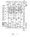
- FIG. l shows the organization of the MOS imager of the invention.
- a typical pixel element is represented by the block 10.
- Each pixel is comprised of a PN diode 12 which is exposed to light from a scene and which generates photoelectric pairs of holes and electrons. This charge is stored in the junction capacitance of the diode or some other storage capacitance until it is time to read the signal from the pixel. The amount of charge generated in each pixel depends upon the intensity of the light from the scene falling on that pixel.
- the charge from each pixel is read out by turning on an MOS transistor 14 associated with each diode.
- the MOS transistor 14 has its source coupled to the cathode of the diode 12 and has its drain coupled to a column video signal line 16.
- the gate of the MOS transistor 14 is coupled to a row address line 18. When the row address line 18 has a predetermined voltage applied thereto exceeding the threshold voltage of the transistor 14, the MOS transistor 14 turns on and the charge stored in the junction capacitance of the diode 12 is coupled through the channel region of the MOS transistor to the column video signal line 16.
- each pixel is conventional and any design and method of making a conventional MOS imager pixel element will suffice for practicing the invention.
- the pixel design taught in the Hitachi paper mentioned above will be satisfactory.
- the cells in either of U.S. Patents 4,143,389 or 4, 155 ,094 will be adequate.
- the layout of the individual pixels on the substrate is comprised of rows of interleaved triangular groups. That is, the pixels 10 , 20 and 22 form a triangular group because pixels 10, 22 and 32 coucled to the first address line 18 are offset front the pixels 20, 30 and 34 in the second row coupled to an address line 36.
- the offset of the rows is such that the pixels coupled to the address line 36 line up with the gaps between the pixels coupled to the address line 18.
- triangular groups of three pixels per group are formed where each pixel in each group is coupled to a different one of three video signal lines which run through the group. For example, the pixel 10 is coupled to the video signal line 16 while the pixels 20 and 22 are coupled to the video signal lines 38 and 40 respectively.
- This pixel arrangement creates the possibility for generating full color video outputs if 3 different color filters are physically placed over the individual pixel elements in each group.
- the video signals on the signal lines 16, 38 and 40 then represent the color content signals of a single, composite color pixel comprised of the individual pixels 10, 20 and 22.
- the color filters can be implemented using any conventional method.
- One known way of providing for a color filter is taught in the paper by Aoki et al cited above.
- There a gelatin layer is deposited over the surface of the substrate after the PN junction diodes and MOS transistors are formed.
- the gelatin layer is then sectionalized using photolithography techniques and each section over a pixel is cyed with an appropriate one of the colors selected.
- the color filters may elso be discrete filters or "may eve" filters placed over the pixels.
- Eastman kodak has published several papers in this area.
- the Boyer patent, U.S. 3,971,065 teaches use of a filter mosaic overlying a CCD area image sensor to produce an array of rows and columns of color responsive photoelements with every other array position occupied by a green-sensitive element serving to detect luminance.
- Red sensitive "chrominance" elements alternate with the luminance detecting elements in every other row while blue sensitive chrominance elements alternate with the luminance elements in the remaining, alternate rows.
- the luminance and chrominance signals from pairs of the rows provide red, blue and green information with green predominating.
- the Dillon patent 4,047,203 teaches an array wherein every other position of the array of horizontal rows and vertical columns of color responsive pixels is also occupied by a green-sensitive, luminance element.
- the chreminance elements of each row alternate between red and blue along the row so that a pattern of four successive elements, two of which are luminance elements and two of which are different chrominance elements, repeats along the length of each row with one element of horizontal displacements from row to row.
- the monochrome or color versatility is lent by virtue of the use of five video cutput lines and two horizontal shift registers, one coupled to the top of the video Signal lines and one coupled to the bottoms of the signal lines.
- Two video output lines 41 and 42 carry the monochrome video signals.
- the output line 41 is coupled to every other one of the video signal lines, i.e., lines 16, 40, and 46.
- the other video output line 42 is coupled to the remaining ones of the video signal lines 38, 44 and 48.
- a horizontal shift register 44 causes selected ones of the video signal lines 16, 38, 40, 44, 46 and 48 to be coupled to the video output lines 41 and 42 by the switching action of MOS transistors 46-51.
- the horizontal shift register 44 has a plurality of cutputs each of which is coupled to the gates of two of the MOS transistors 46-51.
- the MOS transistors 46-51 each have their sources and drains coupled between one of the video signal lines 16, 38, 40, 44, 46 and 48 and one of the video output lines 41 or 42.
- two of the video signal lines 16, 38, 40, 44, 46 and 48 can be coupled to the two video output lines 41 or 42.
- another two of the transistors 46-51 are turned on as a different output from the horizontal shift register 44 is activated. This couples a different two of the video signal lines to the output lines 41 and 42.
- the horizontal shift register 44 can be any conventional shift register of either the CCD type with driver circuits, flip-flop variety, inverter chains, dynamic source follower chains, or any other known design where successive outputs can be sequentially activated however the CCD type is preferred.
- the structure and Operation of shift registers is well-known in the art.
- the horizontal shift register 44 is a two-phase shift register which shifts a single pulse through under the influence of two-phased clock signals ⁇ 11 and ⁇ 12 .
- the MOS transistors 46 and 47 are turned on thereby coupling the vertical signal lines 16 and 38 to the video output lines 41 and 42 respectively.
- the transistors 48 and 49 are turned on and the video signal lines 40 and 44 are thereby coupled to the video output lines 41 and 42.
- a second horizontal shift register 56 causes coupling between the video signal lines 16, 38, 40, 44, 46 and 48 and three color video output lines 57, 58 and 59.
- the second a horizontal shift register 56 can be the same structure and operate the same as the horizontal shift register 44 except that its output lines are each coupled to the gates of three switching transistors instead of only two as in the case of the shift register 44. That is, an output line 60 is coupled to each of the gates of three MOS switching transistors 61-63. When a pulse or charge packet shifts past the output line 60, the three transistors 61-63 all turn on thereby coupling the video signal lines 16, 38 and 40 to the color video outout lines 57-59 respectively.
- the output line 64 operates in the same manner in conjunction with switching transistors 65-67 and video signal lines 44, 46 and 48.
- the reading of the image array can be accomplished in several ways by virtue of the use of two vertical shift registers which are coupled to alternate address lines in the array.
- a vertical shift register 68 having the same structure as the horizontal shift registers 44 and 56, has its outputs coupled to every other address line in the array. That is, the outputs from the vertical shift register 68 are the address lines 18 and 69-71. These address lines are coupled to the gates of the MOS switching transistors for the pixels in every other row.
- the even rows address lines are the output lines of a vertical shift register 72.
- the vertical shift register 72 has the same structure as the horizontal shift registers and 44 and operates in the same manner.
- a variety of scanning modes are available by virtue of the above defined organization for the imager. For example, in monochrome operation, non-interlaced, interlaced or pseudo-interlaced readout is available. Monochrome operation is achieved where there are no color filters over the image array and where the horizontal shift register 56 is deactivated such as by closing switches 74 and 76. As practical matter the switches 74 and 76 are symbolic only and they represent any of a number of different possibilities for deactivating the shift register. Typically the switches 74 and 76 would be MOS switching transistors that are connected either to disconnect the clock signals ⁇ 21 and ⁇ 22 from the clock inputs of the horizontal shift register 56 or to ground the clock signals.
- the horizontal shift register 44 has a similar set of switches 106 and 108 to deactivate it for color operation. With the horizontal shift register 56 deactivated, the switching transistors 61-63 and 65-67 are open circuits and the video output lines 57-59 are therefore deactivated. This leaves only the output lines 41 and 42 activated for monochrome operation.
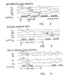
- Monochrome readout occurs in the non-interlaced mode as shown in Figure 2 and described below.
- the non-interlace mode means that first an even row is read out and then the next odd row is read out. This even-odd-even-odd read-cut continues until the entire array has been read out.
- this sequence of events is shown inferentially by the relationships depicted between the signals shown.
- the ⁇ 41 and ⁇ 42 signals drive the vertical shift register 68 in the known manner for two-phase registers.
- the pulses 78 and 80 represent the two pulses necessary to move the pulse or charge packet from one register stage to the next.
- the pulses 78 and 80 can be thought of as transferring the single pulse or charge packet in the vertical shift register 68 into the first register stage so as to charge the first odd address line 18.
- the first odd address line 18 When the first odd address line 18 is charged with the appropriate polarity of charge for the types of switching transistors such as the transistor 14, switching transistors 14, 82 and 84 turn on. For N-channel technology, a positive charge on the address lines will turn on the transistors in each pixel connected to the positively charged line.
- the switching transistors of the first address line 18 turn on, the charge stored in each diode junction capacitance in the associated pixels is dumped into the associated one of the video signal lines 16, 40 and 46. That is, the charge stored in the junction capacitance of the diode 12 is dumped into the video signal line 16 and so on for the other pixels associated with the address line 18.
- the signals on the video signal lines 16, 40 and 46 must be connected to the black and white video output line 41. This happens sequentially under the influence of the horizontal shift register 44 which is driven by the clock signals ⁇ 11 and ⁇ 12 .
- These clock signals are represented by the numerous vertical lines within the rectangular region 86 in Figure 2. These lines represent two clock pulses ⁇ 11 and ⁇ 12 for each output line 52, 54, etc. from the shift register 44.
- the transistor 46 turns on and the video signal line 16 is coupled to the video output line 41.
- a video output signal can then be read from the video output line 41 representing the light intensity falling on the pixel consisting of the transistor 14 and the diode 12.
- the horizontal shift register 44 turns on the transistor 48 and the transistor 46 will turn off. At that time, the video signal from the pixel comprised of the transistor 82 and the diode 88 is coupled through the video signal line 40 and the transistor 48 to the video output line 41.
- the horizontal shift register 44 turns on the transistor 50 and turns off the transistor 48 thereby coupling the pixel comprised of the transistor 84 and the diode 90 to the video output line 41.
- clock pulses 92 and 94 occur in the signals ⁇ 31 and ⁇ 32 . These pulses represent the first transfer of the single pulse or charge packet in the vertical shift register 72. These two pulses cause the charge packet to be transferred into the register stage inside the shift register 72 which is associated with the first even address line 36. Thus all the switching transistors connected to the address line 36 are turned on.
- the horizontal shift register 44 then sweeps out all the signals from the pixels connected to the address line 36 by turning on in sequence, the transistors 47, 49 and 51 respectively connected to the video signal lines 38, 44 and 48. This process of clocking cut the signals is represented by the vertical lines inside the rectangular region 96 in Figure 2 representing the individual clock pulses ⁇ 11 and ⁇ 12 . This pattern is repeated for all the rows in the array.
- Figure 3 represents the interlaced readout mode for monochrome operation. Again the horizontal shift register 56 is deactivated by the switches 74 and 76. In the interlace mode, first all the odd rows are read out for one field and then all the even rows are read out for the next field. This is indicated in Figure 3 by the absence of any pulses in the ⁇ 31 and ⁇ 32 signals until the ⁇ 41 and ⁇ 42 clock pulses have activated each of the odd address lines connected to the vertical shift register 68. The first field is read out between the times t 1 and t 2 . The next field readout begins after the time t 2 upon the occurrence of the pulses 98 and 99 in the signals ⁇ 31 and ⁇ 32 .
- Figure 4 represents the pseudo-interlace, monochrome mode of operation.
- the odd and even rows are read out simultaneously as pairs. This is represented in Figure 4 by the simultaneous occurrence of the pulses in the ⁇ 41 and ⁇ 31 signals and the simultaneous occurrence of the pulses in the and ⁇ 32 signals.
- the simultaneous occurrence of pulses 101 and 103 causes the first odd address line 13 and the first even address line 36 to be simultaneously charged so as to turn on all the switching transistors connected to these two rows.
- the ⁇ 11 and ⁇ 12 pulses represented by the vertical lines in the rectangular area 104 then sweep the individual pixel signals out on the video output lines 41 and 42.
- the odd pixels connected to the address line 18 are swept out on the video output line 41 while the even pixels connected to the address line 36 are simultaneously swept out on the video output line 42.
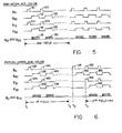
- Figure 5 is a timing diagram for the non-interlace, color mode of operation.
- the horizontal shift register 44 is deactivated by the action of circuitry represented by switches 106 and 108 similar to the circuitry represented by the switches 74 and 76.
- the video output lines 57-59 are activated.
- the color mode three pixels are lumped together as one composite pixel and each pixel in the trio generates one of the three primary color signals in the composite video.
- the non-interlace mode means each row is read out in the sequence odd-even-odd. until all rows have been read out.
- the non-interlace, color readout occurs by simultaneously activating both the odd and the even row address lines for each row of composite color pixels.
- the vertical lines within the region 118 of the representation of the signals ⁇ 21 and ⁇ 22 in Figure 5 represent the individual pulses from the horizontal shift register 56 which activate the output lines 60 and 64 and the associated switching transistors.
- the pulse which activates the line 60 turns on the transistors 61-63 which couples the video signal lines 16, 38 and 40 to the video output lines 57-59 respectively. This process of coupling all the video signal lines in the array to the video output lines 57-59 continues during the duration of the pulses 112 and 116 until all the video signal lines in the array have been coupled in turn to their respective color video output lines 57-59.
- the next row of composite color pixels is read out when pulses 120 and 122 in the ⁇ 41 and ⁇ 42 signals and the pulses 124 and 126 are simultaneously active thereby activating the next pair of row address lines 69 and 128.
- the pulses represented by the region 130 of the ⁇ 21 and ⁇ 22 signals cause each of the trios of video signal lines in the array to be coupled to the color video output lines 57-59 in turn beginning with the trio of line 16, 38 and 40. This process continues until all the pixels are read.
- Figure 6 is a timing diagram of the pseudo-interlace mode of color operation for the invention.
- the horizontal shift register 44 is deactivated by the action of the circuitry represented by the switches 106 and 108.
- the color output lines 57-59 are thus activated and are coupled to trios of the video signal lines in the same manner as described in connection with Figure 5.
- the difference in operation between Figure 5 and Figure 6 is that in Figure 5 during each field both of the row address line for each row of composite color pixels are simultaneously activated.
- one of the row address activation signals lags the other by one period such that the pairing of pulses is different in every other field. That is, the first field in figure 6 extends from t 1 to t 2 and the second field begins at t 4 .
- the simultaneous occurrence of the pulses 132 and 134 in the signals ⁇ 41 and ⁇ 31 and the simultaneous occurrence of the pulses 136 and 138 in the signals ⁇ 42 and ⁇ 32 respectively indicate that in this first field the row address lines 18 and 36 are energized as a pair.
- the simultaneous occurrence of the pulses 140 and 142 in the ⁇ 41 and ⁇ 31 and the pulses 144 and 146 in ⁇ 42 and ⁇ 32 indicate that for readout of the next row of composite color pixels, the row address lines 69 and 128 are activated simultaneously as a pair.
- the pulses in the signals ⁇ 31 and ⁇ 32 are staggered by one cycle from the pulses in the signals ⁇ 41 and ⁇ 42 . That is, it can be seen that the pulse 148 at the time t 3 has no simultaneous counterpart in the signal ⁇ 31 at time t 3 . Likewise the pulse 150 in ⁇ 42 has no counterpart in the signal ⁇ 32 . However at time t 4 the readout of field two commences. During this readout the simultaneous occurrence of the pulses 152 and 154 and the simultaneous occurrence of the pulses 156 and 158 indicates that different pairings of simultaneous row address line activations are occurring. For example the pulses 152, 154, 156 and 158 simultaneously activate the row address lines 69 and 36.
- the signals ⁇ 41 , ⁇ 42 , ⁇ 31 and ⁇ 32 driving the vertical shift registers 68 and 72 and the signals ⁇ 11 , ⁇ 12 , ⁇ 21 and ⁇ 22 driving the horizontal shift registers 44 and 56 are generated by conventional clock logic 160.
- the design of this clock logic 160 is not critical to the invention and any design which supplies the signals shown in Figures 2-6 in the relationships there shown will suffice for purposes of the invention.
- the pattern of signals generated by the clock logic 160 and their relationships can be set by any conventional means such as by supplying external signals to the clock logic to set internal latches to define the desired mode. Alternatively this could be done by blowing fuses in the clock logic 160 during fabrication as with a laser by techniques similar to the techniques used redundant to replace defective circuits in integrated memories by patching in redundant circuits on the die.
Landscapes
- Engineering & Computer Science (AREA)
- Multimedia (AREA)
- Signal Processing (AREA)
- Transforming Light Signals Into Electric Signals (AREA)
- Solid State Image Pick-Up Elements (AREA)
- Color Television Image Signal Generators (AREA)
Applications Claiming Priority (2)
| Application Number | Priority Date | Filing Date | Title |
|---|---|---|---|
| US06/584,855 US4658287A (en) | 1984-02-29 | 1984-02-29 | MOS imaging device with monochrome-color compatibility and signal readout versatility |
| US584855 | 1996-01-11 |
Publications (2)
| Publication Number | Publication Date |
|---|---|
| EP0157660A2 true EP0157660A2 (de) | 1985-10-09 |
| EP0157660A3 EP0157660A3 (de) | 1987-12-02 |
Family
ID=24339061
Family Applications (1)
| Application Number | Title | Priority Date | Filing Date |
|---|---|---|---|
| EP85400246A Withdrawn EP0157660A3 (de) | 1984-02-29 | 1985-02-14 | MOS-Bildaufnahmeanordnung mit Schwarzweiss- und Farbvereinbarkeit und verschiedene Ausleseverfahren zur Anpassungsfähigkeit |
Country Status (4)
| Country | Link |
|---|---|
| US (1) | US4658287A (de) |
| EP (1) | EP0157660A3 (de) |
| JP (1) | JPS60206169A (de) |
| CA (1) | CA1228667A (de) |
Cited By (4)
| Publication number | Priority date | Publication date | Assignee | Title |
|---|---|---|---|---|
| US4692794A (en) * | 1985-02-18 | 1987-09-08 | Fuji Photo Film Co., Ltd. | Color image sensor with picture elements each comprising an M×N matrix of red, green, and blue photoelectric conversion elements featuring controllable charge storage time and selective readout for each color |
| US4709259A (en) * | 1985-05-08 | 1987-11-24 | Fuji Photo Film Co., Ltd. | Color image sensor |
| US4768085A (en) * | 1984-12-28 | 1988-08-30 | Canon Kabushiki Kaisha | Image sensing apparatus |
| EP1592229A2 (de) * | 2004-04-23 | 2005-11-02 | Sony Corporation | Festkörperbildaufnahmevorrichtung |
Families Citing this family (28)
| Publication number | Priority date | Publication date | Assignee | Title |
|---|---|---|---|---|
| JPS61290408A (ja) * | 1985-06-18 | 1986-12-20 | Fuji Xerox Co Ltd | カラ−密着型イメ−ジセンサおよびその製造方法 |
| US4764813A (en) * | 1985-09-20 | 1988-08-16 | Fuji Photo Film Co., Ltd. | Variable order and period solid state image pickup device |
| US4802001A (en) * | 1985-09-20 | 1989-01-31 | Fuji Photo Film Co., Ltd. | Micro filter arrangement in an interlaced solid-state image pickup element |
| JPS63245073A (ja) * | 1987-03-31 | 1988-10-12 | Canon Inc | 撮像装置 |
| US4959723A (en) * | 1987-11-06 | 1990-09-25 | Canon Kabushiki Kaisha | Solid state image pickup apparatus having multi-phase scanning pulse to read out accumulated signal |
| JPH03190171A (ja) * | 1989-12-12 | 1991-08-20 | Samsung Electron Devices Co Ltd | Ccd型固体撮像素子 |
| DE3824639C2 (de) * | 1988-07-20 | 1993-11-18 | Geutebrueck Videotechnik Gmbh | Optische Überwachungseinrichtung |
| JPH0271684A (ja) * | 1988-09-06 | 1990-03-12 | Mitsubishi Electric Corp | 固体撮像デバイス駆動装置 |
| US5262850A (en) * | 1988-09-20 | 1993-11-16 | Canon Kabushiki Kaisha | Photoelectric converting device having reduced line sensor space |
| JP2891550B2 (ja) * | 1991-01-11 | 1999-05-17 | 三菱電機株式会社 | イメージセンサ |
| US5111263A (en) * | 1991-02-08 | 1992-05-05 | Eastman Kodak Company | Charge-coupled device (CCD) image sensor operable in either interlace or non-interlace mode |
| JPH0654259A (ja) * | 1992-07-31 | 1994-02-25 | Sony Corp | Fit型固体撮像装置 |
| US5521640A (en) | 1994-10-31 | 1996-05-28 | At&T Global Information Solutions Company | Color image array scanner with high resolution monochrome mode |
| JP3511772B2 (ja) * | 1995-12-21 | 2004-03-29 | ソニー株式会社 | 固体撮像素子、固体撮像素子の駆動方法、カメラ装置及びカメラシステム |
| EP0809395A3 (de) * | 1996-05-22 | 1998-03-18 | Eastman Kodak Company | CMOS APS mit Matrix-Adressierung und einer kompakten Pixelperiode |
| KR100215307B1 (ko) * | 1996-12-30 | 1999-08-16 | 유무성 | 프로그레시브 씨씨디를 메모리로 활용한 디지탈 스틸 카메라 |
| US6452632B1 (en) | 1997-01-31 | 2002-09-17 | Kabushiki Kaisha Toshiba | Solid state image sensor and video system using the same |
| JP3548410B2 (ja) * | 1997-12-25 | 2004-07-28 | キヤノン株式会社 | 固体撮像装置および固体撮像装置の信号読み出し方法 |
| JPH11196427A (ja) * | 1997-12-26 | 1999-07-21 | Canon Inc | 単板カラー撮像装置 |
| US6466265B1 (en) * | 1998-06-22 | 2002-10-15 | Eastman Kodak Company | Parallel output architectures for CMOS active pixel sensors |
| US6707496B1 (en) * | 1999-09-15 | 2004-03-16 | Omnivision Technologies, Inc. | CMOS sensor having analog delay line for image processing |
| US20020071041A1 (en) * | 2000-12-07 | 2002-06-13 | Pine Joshua I. | Enhanced resolution mode using color image capture device |
| US7859581B2 (en) * | 2003-07-15 | 2010-12-28 | Eastman Kodak Company | Image sensor with charge binning and dual channel readout |
| JP4468052B2 (ja) * | 2004-04-08 | 2010-05-26 | キヤノン株式会社 | 撮像装置及び撮像装置の制御方法 |
| JP2005333265A (ja) * | 2004-05-18 | 2005-12-02 | Olympus Corp | 固体撮像素子および装置 |
| JP4732709B2 (ja) * | 2004-05-20 | 2011-07-27 | 株式会社半導体エネルギー研究所 | シフトレジスタ及びそれを用いた電子機器 |
| JP4959207B2 (ja) * | 2006-03-06 | 2012-06-20 | ソニー株式会社 | 固体撮像装置 |
| JP5101972B2 (ja) * | 2007-10-02 | 2012-12-19 | オリンパス株式会社 | 固体撮像装置 |
Family Cites Families (5)
| Publication number | Priority date | Publication date | Assignee | Title |
|---|---|---|---|---|
| JPS5379430A (en) * | 1976-12-24 | 1978-07-13 | Hitachi Ltd | Color solid state pickup device |
| JPS5597781A (en) * | 1979-01-19 | 1980-07-25 | Matsushita Electric Ind Co Ltd | Color television camera |
| JPS5850881A (ja) * | 1981-09-21 | 1983-03-25 | Hitachi Ltd | 撮像装置 |
| FR2522235B1 (fr) * | 1982-02-19 | 1986-02-21 | Thomson Brandt | Camera de television en couleurs comportant un filtre matriciel trichrome |
| FR2533056B1 (fr) * | 1982-09-14 | 1987-05-15 | Thomson Csf | Imageur a transfert de lignes et camera de television comportant un tel imageur |
-
1984
- 1984-02-29 US US06/584,855 patent/US4658287A/en not_active Expired - Lifetime
-
1985
- 1985-02-14 EP EP85400246A patent/EP0157660A3/de not_active Withdrawn
- 1985-02-27 JP JP60036710A patent/JPS60206169A/ja active Pending
- 1985-02-28 CA CA000475359A patent/CA1228667A/en not_active Expired
Cited By (4)
| Publication number | Priority date | Publication date | Assignee | Title |
|---|---|---|---|---|
| US4768085A (en) * | 1984-12-28 | 1988-08-30 | Canon Kabushiki Kaisha | Image sensing apparatus |
| US4692794A (en) * | 1985-02-18 | 1987-09-08 | Fuji Photo Film Co., Ltd. | Color image sensor with picture elements each comprising an M×N matrix of red, green, and blue photoelectric conversion elements featuring controllable charge storage time and selective readout for each color |
| US4709259A (en) * | 1985-05-08 | 1987-11-24 | Fuji Photo Film Co., Ltd. | Color image sensor |
| EP1592229A2 (de) * | 2004-04-23 | 2005-11-02 | Sony Corporation | Festkörperbildaufnahmevorrichtung |
Also Published As
| Publication number | Publication date |
|---|---|
| EP0157660A3 (de) | 1987-12-02 |
| CA1228667A (en) | 1987-10-27 |
| US4658287A (en) | 1987-04-14 |
| JPS60206169A (ja) | 1985-10-17 |
Similar Documents
| Publication | Publication Date | Title |
|---|---|---|
| US4658287A (en) | MOS imaging device with monochrome-color compatibility and signal readout versatility | |
| US5410349A (en) | Solid-state image pick-up device of the charge-coupled device type synchronizing drive signals for a full-frame read-out | |
| US6452634B1 (en) | Charge transfer device and method of driving the same, and solid state imaging device and method of driving the same | |
| KR100331995B1 (ko) | 촬상장치에서 복수의 화소에 의해 공유되는 각 회로의 화소내의배치 | |
| US4117514A (en) | Solid state imaging device | |
| US6388278B1 (en) | Solid state image pickup device and its driving method | |
| US6496224B2 (en) | Imaging device including thinned read out mode and all pixel read out mode | |
| US7218348B2 (en) | Solid-state electronic imaging device and method of controlling opertion thereof | |
| US4641183A (en) | Image pick-up apparatus | |
| JP2002270809A (ja) | 固体撮像装置及びその制御方法 | |
| US4322740A (en) | Solid-state color imaging camera | |
| KR0186201B1 (ko) | 컬러 선형 씨씨디 영상소자 및 이의 구동방법 | |
| US7379107B2 (en) | Image sensor for still or video photography | |
| US5796433A (en) | Multiple-frame CCD image sensor with overlying photosensitive layer | |
| US4675887A (en) | Solid state imaging device and method with row-by-row charge transfer | |
| GB2261113A (en) | Solid-state image sensor | |
| US4862487A (en) | Solid-state imaging device | |
| US8045025B2 (en) | Image pickup device adaptable to display fewer vertical pixels | |
| JPS60134675A (ja) | 固体撮像デバイスおよびその製造方法 | |
| JP3367852B2 (ja) | 固体撮像装置 | |
| JP3089507B2 (ja) | 固体撮像素子および信号電荷転送方法 | |
| US5283633A (en) | Solid state image pickup device in which picture elements of green are generated in vertical charge transfer paths | |
| US5978026A (en) | Solid-state image pickup device | |
| JP2994427B2 (ja) | 画像読取装置 | |
| JPH0574992B2 (de) |
Legal Events
| Date | Code | Title | Description |
|---|---|---|---|
| PUAI | Public reference made under article 153(3) epc to a published international application that has entered the european phase |
Free format text: ORIGINAL CODE: 0009012 |
|
| AK | Designated contracting states |
Designated state(s): DE FR GB IT NL |
|
| PUAL | Search report despatched |
Free format text: ORIGINAL CODE: 0009013 |
|
| RHK1 | Main classification (correction) |
Ipc: H04N 9/04 |
|
| AK | Designated contracting states |
Kind code of ref document: A3 Designated state(s): DE FR GB IT NL |
|
| 17P | Request for examination filed |
Effective date: 19880520 |
|
| 17Q | First examination report despatched |
Effective date: 19900314 |
|
| STAA | Information on the status of an ep patent application or granted ep patent |
Free format text: STATUS: THE APPLICATION IS DEEMED TO BE WITHDRAWN |
|
| 18D | Application deemed to be withdrawn |
Effective date: 19900725 |
|
| RIN1 | Information on inventor provided before grant (corrected) |
Inventor name: CHEN, CHENG-WEI |