EP0158515A2 - Auswahldiversitysystem mit Kodekorrektur/Auswahlschaltung zum Empfang eines trägerfrequenten PSK oder QAM differentiell kodierten Signals - Google Patents
Auswahldiversitysystem mit Kodekorrektur/Auswahlschaltung zum Empfang eines trägerfrequenten PSK oder QAM differentiell kodierten Signals Download PDFInfo
- Publication number
- EP0158515A2 EP0158515A2 EP85302381A EP85302381A EP0158515A2 EP 0158515 A2 EP0158515 A2 EP 0158515A2 EP 85302381 A EP85302381 A EP 85302381A EP 85302381 A EP85302381 A EP 85302381A EP 0158515 A2 EP0158515 A2 EP 0158515A2
- Authority
- EP
- European Patent Office
- Prior art keywords
- digital signals
- sequences
- psk
- demodulated digital
- code
- Prior art date
- Legal status (The legal status is an assumption and is not a legal conclusion. Google has not performed a legal analysis and makes no representation as to the accuracy of the status listed.)
- Granted
Links
- 108010076504 Protein Sorting Signals Proteins 0.000 claims abstract description 3
- 238000010586 diagram Methods 0.000 description 4
- 238000000034 method Methods 0.000 description 4
- 230000027311 M phase Effects 0.000 description 2
- 238000011084 recovery Methods 0.000 description 2
- 230000005540 biological transmission Effects 0.000 description 1
- 230000001427 coherent effect Effects 0.000 description 1
- 238000004891 communication Methods 0.000 description 1
- 239000000470 constituent Substances 0.000 description 1
- 238000001514 detection method Methods 0.000 description 1
- 230000010363 phase shift Effects 0.000 description 1
- 230000008054 signal transmission Effects 0.000 description 1
Images


Classifications
-
- H—ELECTRICITY
- H04—ELECTRIC COMMUNICATION TECHNIQUE
- H04L—TRANSMISSION OF DIGITAL INFORMATION, e.g. TELEGRAPHIC COMMUNICATION
- H04L1/00—Arrangements for detecting or preventing errors in the information received
- H04L1/02—Arrangements for detecting or preventing errors in the information received by diversity reception
-
- H—ELECTRICITY
- H04—ELECTRIC COMMUNICATION TECHNIQUE
- H04L—TRANSMISSION OF DIGITAL INFORMATION, e.g. TELEGRAPHIC COMMUNICATION
- H04L27/00—Modulated-carrier systems
- H04L27/18—Phase-modulated carrier systems, i.e. using phase-shift keying
- H04L27/22—Demodulator circuits; Receiver circuits
- H04L27/227—Demodulator circuits; Receiver circuits using coherent demodulation
Definitions
- the present invention relates to a diversity system of selection type for receiving and demodulating with a plurality of receiver sections a multi-phase PSK (phase shift keying) or multi-level QAM (quadrature amplitude modulation) wave carrying differentially encoded signals, and for selecting the signals with the lowest bit error rate (BER) out of the demodulated signals.
- a multi-phase PSK phase shift keying
- multi-level QAM quadrature amplitude modulation
- a diversity system of selection type comprising N (> 2) receiver means for receiving multi-phase PSK or multi-level QA M waves carrying differentially modulo-M (equal to or more than 2) encoded digital signals and providing N sequences of demodulated digital signals by phase-detecting the waves with a recovered carrier wave, and selector means for selecting out of the N sequences of demodulated digital signals one with a low bit error rate, which further includes first means for aligning said selected one of the sequence of demodulated digital signals with other sequences of demodulated digital signals, thereby providing a demodulated digital signal sequence retaining said differential encoding, as the output of the selector means.
- FIG. 1 is a block diagram illustrating an example cf an intermediate relay station structure arranged between terminal stations and, moreover, using a conventional space diversity system of selection type.
- the relay station consists of a receiver section 100 and a transmitter section 101.
- the receiver section 100 comprises a control circuit 6, antennas lla and llb, receivers 12a and 12b, demodulators 13a and 13b, differential decoders 14a and 14b, and a switch 15.
- the control circuit 6 further consists of counters 7a and 7b, an OR gate 8 and an SR (set/reset) flipflop 9.
- the transmitter sections 101 consists a differential encoder 16, a modulator 17, a transmitter 18 and an antenna 19.
- the multi-phase PSK or multi-level QAM waves carrying digital signals having undergone modulo-M (> 2) differential encoding which are transmitted from a terminal station (not shown) , are respectively picked up by the antennas lla and llb, frequency converted by the receivers 12a' and 12b, and supplied to the demodulators 13a and 13b.
- Each of the demodulators 13a and 13b is composed of a carrier recovery circuit, a clock recovery-circuit, a coherent detector for detecting the PSK or QAM wave according to the recovered carrier wave, and a discriminator circuit for level-discriminating the output of the ccherent detector with the recovered clock and providing demodulated digital signals.
- the outputs of these demodulators 13a and 13b i.e., those of the discriminator circuits, are respectively supplied to the differential decoders 14a and 14b to be decoded into the original digital signals.
- the demodulators 13a and 13b include a bit error detector (not shown) each. For details on these bit error detectors, reference may be made to the United States Patent No. 4,188,615, assigned to NEC corporation and issued on February 12, 1980.
- the outputs of these bit error detectors are supplied to the control circuit 6, which generates a control signal for selecting, out of the signals demodulated by the demodulators 13a and 13b, those with a lower BER.
- the counters 7a and 7b count bit error signals; upon having counted them up, set or reset the SR flipflop 9 and at the same time reset both counters 7a and 7b through the OR gate 8.
- the output of the flipflop 9 actuates the switch 15 to select the output of the differential encoder, whose BER is lower.
- the digital signals selected by the switch 15 are differentially encoded by the differential encoder 16, and supplied to the modulator 17 which provides PSK waves.
- the PSK waves are frequency converted by the transmitter 18 and transmitted to another relay station or terminal station (not shown) from the antenna 19.
- Yamazaki et al. "2GHz Digital Radio-Relay System", IEEE International Conference on Communication, Vol. 1, pp. 5.5.1-5.5.5, 1979.
- characters P and Q represent the codes of two sequences of demodulated data from one of two demodulators at the same point of time to be differentially encoded and P and Q, those of data sequences from the other, P and Q are expressed by P and Q, as shown in Fig. 2.
- the codes P and Q can be always made identical to the codes P and Q irrespective of whichever of the conditions 1 to 4, switching (selection) at the intermediate relay station will be made possible without losing the differential encoding function, and the complex differential decoders and encoders will be dispensed with.
- the code coincidence is readily carried out by repeating the process comprising the following steps: (1) comparing P and P (or Q and Q), (2) actuating a modulo-4 (modulo M) counter in response to the comparing output, and (3) converting P and Q in the input conditions of 1 to 4 into P and Q in response to the counter output. Accordingly, at most four repetitions of the process can cause P and Q to coincide with P and Q. Where the modulus is M, exactly the same result can be achieved if there are provided a code-converter for M input conditions and an modulo-M counter.
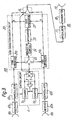
- FIG. 3 illustrates an intermediate relay station in which is used a diversity system including a code correction/switch circuit according to the present invention.
- the same constituent elements as in FIG. 1 are represented by respectively the same reference numerals.
- the receiver section 110 includes a code correction/switch circuit 20, which is a characteristic feature of the present invention.
- the circuit 20 comprises code converters 21a and 21b, a code comparator 22, an integrator 23, a modulo-4 counter 24 and a switch 25.
- phase ambiguity is detected by the code comparator 22 on the basis of differences between code sequences X and Y, and the detection output is determined by the integrator 23 to be either a simple code error or a disparity due to a phase ambiguity, the determination output further actuating the modulo-4 counter 24.
- the output of the modulo-4 counter 24 is switch-connected to the code converters 21a and 21b via the switch 25, which, as is evident from the figure, is turned in a reverse position to the switch 15.
- the phase ambiguity is so corrected as to bring into coincidence with the currently selected code sequence the-other code sequence, so that continuous data can be provided from the output of the switch 15, irrespective of the position of the switch 15.
- the positions of the switches 15 and 25 in FIG. 3 represent a case in which the output of the demodulator 13a is higher in BER than that of the demodulator 13b.
- FIG. 4 illustrates an example of the code converter 21a (or 21b) of FIG. 3 where M is 4.
- the converter 21a or 21b comprises gates 31 and 33 for outputting normal and reverse phases, respectively, a selection switch circuit 32 and flipflops 34 and 35.
- the outputs P and Q of the demodulator 13a are supplied to the gates 31 and 33, and converted into the four pairs of codes 1 to 4, i.e., (P, Q), (Q, -P), (-P, -Q) and (-Q, P), as shown in FIG. 2.
- the selection switch circuit 32 which may be Motorola's MC 10174 for instance, selects one of the four code pairs in accordance with the outputs of the flipflops 34 and 35. The selecting process is continued until the outputs of the two code converters 21a and 21b coincide with each other.
- flipflops 34 and 35 read the outputs A' and B' of the modulo-4 counter 24 in response to a clock pulse CLK from a clock recovery circuit in the demodulator 13a or 13b.
- the switch 25 switches both the clock pulse CLK and the output of the counter 24. Accordingly, if switch 25 is connected as represented by the solid line in FIG. 3, the flipflops 34 and 35 in the code converter 21a which is subject to code correction read and retain the output of the counter 24 bit by bit in response to the clock pulse CLK. Meanwhile, the flipflops of the code converter 21b, not subject to code correction, are supplied with neither the clock pulse PSK nor the output of the counter 24, and accordingly retain the output of the counter 24 before switching by the switch 25. Therefore, only the selection switch circuit 32 of the code converter subject to code correction is actuated by the output of the counter 24.
- FIG. 5 illustrates an example of specific circuitry of the code comparator 22, integrator 23 and counter 24.
- the outputs X and Y of the code converters 21a and 21b in FIG. 3 or 4 are supplied to the code comparator 22.
- the outputs X and Y as is evident from FIG. 4, consists of two sequences each when M is 4, only one of the two sequences is used in the embodiment of FIG. 5 to simplify the code comparator 22.
- the outputs X and Y are read by flipflops 221 and 222 of the code comparator 22 in accordance with the aforementioned clock pulse CLK, and their coincidence or non-coincidence is determined by an Exclusive-OR/NOR gate 223.
- a coincidence signal is supplied to a counter 231 of the integrator 23, while a non-coincidence signal is fed to a counter 232 of same.
- the counter 231 will be reset. If they continue to be non-coincident for a certain length of time, the output of the counter 232 will rise to a high level to open the gate 233, and the non-coincidence signal fed to the other input terminal will pass the gate 233 to alter the outputs A' and B' of the flipflops 241 and 241 cyclically. These outputs A' and B' are read into the flipflops 34 and 35 via the switch 25 to sequentially select one or another of the aforementioned four code pairs 1 to 4, and this process is repeated until the output X of the code converter 21a coincides with the output Y of the code converter 21b.
- the switch 15 of the relay station can be turned back and forth while keeping the differential encoding function at the terminal stations preceding the relay station.
- the transmitter section 111 requires nothing like the encoder 16 in FIG. 1.
- the present invention makes it possible to consecutively switch on (select), as desired, one of plural reception systems among N reception systems having M phase ambiguities. Moreover, since only phase ambiguities are corrected without losing the differential encoding function, differential decoders and differential encoders, which would complicate the structure, can be dispensed with. Therefore, even where no differential decoder or differential encoder at the relay station can be used, differential encoding at the terminal station is made possible, and the hardware structure can be relatively simplified.
Landscapes
- Engineering & Computer Science (AREA)
- Computer Networks & Wireless Communication (AREA)
- Signal Processing (AREA)
- Radio Transmission System (AREA)
- Digital Transmission Methods That Use Modulated Carrier Waves (AREA)
Applications Claiming Priority (2)
| Application Number | Priority Date | Filing Date | Title |
|---|---|---|---|
| JP67349/84 | 1984-04-06 | ||
| JP59067349A JPS60212048A (ja) | 1984-04-06 | 1984-04-06 | 符号修正型切替方式 |
Publications (3)
| Publication Number | Publication Date |
|---|---|
| EP0158515A2 true EP0158515A2 (de) | 1985-10-16 |
| EP0158515A3 EP0158515A3 (en) | 1986-06-25 |
| EP0158515B1 EP0158515B1 (de) | 1989-08-16 |
Family
ID=13342448
Family Applications (1)
| Application Number | Title | Priority Date | Filing Date |
|---|---|---|---|
| EP85302381A Expired EP0158515B1 (de) | 1984-04-06 | 1985-04-04 | Auswahldiversitysystem mit Kodekorrektur/Auswahlschaltung zum Empfang eines trägerfrequenten PSK oder QAM differentiell kodierten Signals |
Country Status (6)
| Country | Link |
|---|---|
| US (1) | US4663768A (de) |
| EP (1) | EP0158515B1 (de) |
| JP (1) | JPS60212048A (de) |
| AU (1) | AU572054B2 (de) |
| CA (1) | CA1238369A (de) |
| DE (1) | DE3572431D1 (de) |
Cited By (1)
| Publication number | Priority date | Publication date | Assignee | Title |
|---|---|---|---|---|
| CH682363A5 (de) * | 1991-04-29 | 1993-08-31 | Ascom Radiocom Ag |
Families Citing this family (17)
| Publication number | Priority date | Publication date | Assignee | Title |
|---|---|---|---|---|
| JPS60214641A (ja) * | 1984-04-10 | 1985-10-26 | Nec Corp | 時分割多方向通信のスペース・ダイバシティ通信方式 |
| US4823398A (en) * | 1985-12-23 | 1989-04-18 | Kazuya Hashimoto | Diversity receiver |
| JPS62298255A (ja) * | 1986-06-18 | 1987-12-25 | Fujitsu Ltd | 識別装置 |
| GB2194850B (en) * | 1986-09-05 | 1990-10-31 | Philips Nv | Data processing device |
| US4780869A (en) * | 1987-05-20 | 1988-10-25 | Allen-Bradley Company, Inc. | Local area network redundancy system |
| US4942591A (en) * | 1989-03-07 | 1990-07-17 | Agilis Corporation | Multiple phase PSK demodulator |
| US5088113A (en) * | 1990-01-02 | 1992-02-11 | At&T Bell Laboratories | Diversity coded modulation |
| JPH0787445B2 (ja) * | 1990-08-01 | 1995-09-20 | 三菱電機株式会社 | アンテナ選択ダイバーシティ受信装置 |
| US5504779A (en) * | 1992-12-04 | 1996-04-02 | Reliance Electric Industrial Company | Redundancy modem |
| JP2699850B2 (ja) * | 1993-12-28 | 1998-01-19 | 日本電気株式会社 | 復調装置 |
| GB2307152B (en) * | 1995-11-10 | 1999-04-07 | Motorola Ltd | Method and apparatus for enhanced communication capability while maintaining standard channel modulation compatibility |
| JP3288574B2 (ja) * | 1996-02-26 | 2002-06-04 | 松下電器産業株式会社 | データ受信装置 |
| US6041086A (en) * | 1996-04-04 | 2000-03-21 | Lucent Technologies Inc. | Signal decoding for either Manhattan or Hamming metric based Viterbi decoders |
| US6459725B1 (en) * | 1998-07-31 | 2002-10-01 | Qualcomm Incorporated | Wireless repeater with improved diversity |
| JP2001177879A (ja) * | 1999-12-17 | 2001-06-29 | Nec Viewtechnology Ltd | リモコン信号受信装置 |
| WO2008044902A1 (en) * | 2006-10-13 | 2008-04-17 | Electronics And Telecommunications Research Institute | Relaying method of relay station(rs) using a direct relaying zone in multi-hop relay system |
| JP4079197B1 (ja) * | 2007-02-06 | 2008-04-23 | 松下電器産業株式会社 | 受信装置とこれを用いた受信システム |
Family Cites Families (9)
| Publication number | Priority date | Publication date | Assignee | Title |
|---|---|---|---|---|
| US3628149A (en) * | 1968-12-19 | 1971-12-14 | Bell Telephone Labor Inc | Diversity switch for digital transmission |
| JPS5431212A (en) * | 1977-08-15 | 1979-03-08 | Nec Corp | Monitor circuit for digital signal transmission line |
| US4246656A (en) * | 1978-10-24 | 1981-01-20 | Raytheon Company | Diversity switch correlation system |
| FR2462065A1 (fr) * | 1979-07-24 | 1981-02-06 | Thomson Csf | Dispositif de commutation automatique d'equipements de transmission de signaux numeriques et faisceaux hertziens comportant un tel dispositif |
| JPS5654141A (en) * | 1979-10-09 | 1981-05-14 | Nec Corp | Band switching circuit without momentary interruption |
| US4349914A (en) * | 1980-04-01 | 1982-09-14 | Ford Aerospace & Communications Corp. | Bit synchronous switching system for space diversity operation |
| JPS58202642A (ja) * | 1982-05-21 | 1983-11-25 | Nec Corp | スペ−スダイバ−シテイ受信装置 |
| US4506385A (en) * | 1982-12-27 | 1985-03-19 | Rockwell International Corporation | Radio reception path monitor for a diversity system |
| US4615040A (en) * | 1984-06-14 | 1986-09-30 | Coenco Ltd. | High speed data communications system |
-
1984
- 1984-04-06 JP JP59067349A patent/JPS60212048A/ja active Granted
-
1985
- 1985-04-04 CA CA000478387A patent/CA1238369A/en not_active Expired
- 1985-04-04 EP EP85302381A patent/EP0158515B1/de not_active Expired
- 1985-04-04 DE DE8585302381T patent/DE3572431D1/de not_active Expired
- 1985-04-05 US US06/720,221 patent/US4663768A/en not_active Expired - Lifetime
- 1985-04-09 AU AU40927/85A patent/AU572054B2/en not_active Ceased
Cited By (1)
| Publication number | Priority date | Publication date | Assignee | Title |
|---|---|---|---|---|
| CH682363A5 (de) * | 1991-04-29 | 1993-08-31 | Ascom Radiocom Ag |
Also Published As
| Publication number | Publication date |
|---|---|
| CA1238369A (en) | 1988-06-21 |
| EP0158515B1 (de) | 1989-08-16 |
| JPH0230216B2 (de) | 1990-07-05 |
| AU572054B2 (en) | 1988-04-28 |
| DE3572431D1 (en) | 1989-09-21 |
| US4663768A (en) | 1987-05-05 |
| EP0158515A3 (en) | 1986-06-25 |
| AU4092785A (en) | 1985-10-10 |
| JPS60212048A (ja) | 1985-10-24 |
Similar Documents
| Publication | Publication Date | Title |
|---|---|---|
| US4663768A (en) | Diversity system of selection type equipped with a code correction/switch circuit for receiving a PSK or QAM wave carrying differentially encoded signal | |
| US5023889A (en) | Trellis coded multilevel DPSK system with doppler correction for mobile satellite channels | |
| US4099121A (en) | Spatial diversity satellite communications system with error control | |
| US5025455A (en) | Phase ambiguity resolution for offset QPSK modulation systems | |
| CA1110706A (en) | Synchronizing means for a two-way communication system | |
| CA1065020A (en) | High reliability diversity communications system | |
| KR100240869B1 (ko) | 이중 다이버서티 시스템을 위한 데이터 전송 방법 | |
| US5065107A (en) | Phase-locked loop bandwidth switching demodulator for suppressed carrier signals | |
| EP0390351A2 (de) | Verfahren und Einrichtung zur Demodulation von binären PSK-Signalen | |
| JPH0828704B2 (ja) | ユニークワード検出方式 | |
| US4290140A (en) | Combined coherent frequency and phase shift keying modulation system | |
| US4425666A (en) | Data encoding and decoding communication system for three frequency FSK modulation and method therefor | |
| EP0197541B1 (de) | System zur Steuerung der Arbeitsweise eines Modulators/Demodulators | |
| EP1115237B1 (de) | Empfänger für digitale funksignale | |
| US5173926A (en) | Convolutionally-encoded quadrature frequency-modulation system | |
| US7180962B2 (en) | Apparatus and method for demodulation using detection of channel adaptive modulation scheme | |
| CN110098881B (zh) | 宽窄波束信号传输方法、装置及电子设备 | |
| EP1154596B1 (de) | Digitaler Signaldetektor, digitaler Demodulator , Verfahren zur Detektierung eines digitales Signals und Verfahren zur synchronen Detektierung durch einen digitalen Demodulator | |
| WO1997016900A1 (en) | Method and apparatus for symbol timing tracking | |
| CA2286522C (en) | Diversity communication system and method of operation thereof | |
| KR100546801B1 (ko) | 채널 적응형 변조방식 검출을 이용한 복조 장치 및 그 방법 | |
| WO1993012598A1 (en) | Combination of two signals, the second appearing as a noise for the first one | |
| JP2754414B2 (ja) | ダイバーシティ受信回路 | |
| JP3313394B2 (ja) | デジタル多重無線方式におけるビットインタリーブ機能付変復調器 | |
| JPS6342456B2 (de) |
Legal Events
| Date | Code | Title | Description |
|---|---|---|---|
| PUAI | Public reference made under article 153(3) epc to a published international application that has entered the european phase |
Free format text: ORIGINAL CODE: 0009012 |
|
| 17P | Request for examination filed |
Effective date: 19850424 |
|
| AK | Designated contracting states |
Designated state(s): DE FR GB IT |
|
| PUAL | Search report despatched |
Free format text: ORIGINAL CODE: 0009013 |
|
| AK | Designated contracting states |
Kind code of ref document: A3 Designated state(s): DE FR GB IT |
|
| 17Q | First examination report despatched |
Effective date: 19880201 |
|
| GRAA | (expected) grant |
Free format text: ORIGINAL CODE: 0009210 |
|
| AK | Designated contracting states |
Kind code of ref document: B1 Designated state(s): DE FR GB IT |
|
| REF | Corresponds to: |
Ref document number: 3572431 Country of ref document: DE Date of ref document: 19890921 |
|
| ET | Fr: translation filed | ||
| ITF | It: translation for a ep patent filed | ||
| PLBE | No opposition filed within time limit |
Free format text: ORIGINAL CODE: 0009261 |
|
| STAA | Information on the status of an ep patent application or granted ep patent |
Free format text: STATUS: NO OPPOSITION FILED WITHIN TIME LIMIT |
|
| 26N | No opposition filed | ||
| ITTA | It: last paid annual fee | ||
| REG | Reference to a national code |
Ref country code: GB Ref legal event code: IF02 |
|
| PGFP | Annual fee paid to national office [announced via postgrant information from national office to epo] |
Ref country code: GB Payment date: 20020404 Year of fee payment: 18 |
|
| PGFP | Annual fee paid to national office [announced via postgrant information from national office to epo] |
Ref country code: FR Payment date: 20020410 Year of fee payment: 18 Ref country code: DE Payment date: 20020410 Year of fee payment: 18 |
|
| PG25 | Lapsed in a contracting state [announced via postgrant information from national office to epo] |
Ref country code: GB Free format text: LAPSE BECAUSE OF NON-PAYMENT OF DUE FEES Effective date: 20030404 |
|
| PG25 | Lapsed in a contracting state [announced via postgrant information from national office to epo] |
Ref country code: DE Free format text: LAPSE BECAUSE OF NON-PAYMENT OF DUE FEES Effective date: 20031101 |
|
| GBPC | Gb: european patent ceased through non-payment of renewal fee |
Effective date: 20030404 |
|
| PG25 | Lapsed in a contracting state [announced via postgrant information from national office to epo] |
Ref country code: FR Free format text: LAPSE BECAUSE OF NON-PAYMENT OF DUE FEES Effective date: 20031231 |
|
| REG | Reference to a national code |
Ref country code: FR Ref legal event code: ST |