EP0197541B1 - System zur Steuerung der Arbeitsweise eines Modulators/Demodulators - Google Patents
System zur Steuerung der Arbeitsweise eines Modulators/Demodulators Download PDFInfo
- Publication number
- EP0197541B1 EP0197541B1 EP86104775A EP86104775A EP0197541B1 EP 0197541 B1 EP0197541 B1 EP 0197541B1 EP 86104775 A EP86104775 A EP 86104775A EP 86104775 A EP86104775 A EP 86104775A EP 0197541 B1 EP0197541 B1 EP 0197541B1
- Authority
- EP
- European Patent Office
- Prior art keywords
- demodulator
- operation mode
- modulator
- switchover
- mode
- Prior art date
- Legal status (The legal status is an assumption and is not a legal conclusion. Google has not performed a legal analysis and makes no representation as to the accuracy of the status listed.)
- Expired
Links
- 230000005540 biological transmission Effects 0.000 claims description 6
- 238000000034 method Methods 0.000 claims description 5
- 238000001514 detection method Methods 0.000 description 17
- 238000004891 communication Methods 0.000 description 14
- 238000010586 diagram Methods 0.000 description 3
- 238000010295 mobile communication Methods 0.000 description 3
- 230000001360 synchronised effect Effects 0.000 description 3
- 241001227713 Chiron Species 0.000 description 1
- 210000004899 c-terminal region Anatomy 0.000 description 1
- 238000010276 construction Methods 0.000 description 1
- 230000001419 dependent effect Effects 0.000 description 1
- 230000007257 malfunction Effects 0.000 description 1
- 230000010363 phase shift Effects 0.000 description 1
- 238000011084 recovery Methods 0.000 description 1
- 238000005070 sampling Methods 0.000 description 1
- 230000008054 signal transmission Effects 0.000 description 1
Images

Classifications
-
- H—ELECTRICITY
- H04—ELECTRIC COMMUNICATION TECHNIQUE
- H04L—TRANSMISSION OF DIGITAL INFORMATION, e.g. TELEGRAPHIC COMMUNICATION
- H04L5/00—Arrangements affording multiple use of the transmission path
- H04L5/14—Two-way operation using the same type of signal, i.e. duplex
- H04L5/1438—Negotiation of transmission parameters prior to communication
-
- H—ELECTRICITY
- H04—ELECTRIC COMMUNICATION TECHNIQUE
- H04L—TRANSMISSION OF DIGITAL INFORMATION, e.g. TELEGRAPHIC COMMUNICATION
- H04L27/00—Modulated-carrier systems
- H04L27/18—Phase-modulated carrier systems, i.e. using phase-shift keying
- H04L27/22—Demodulator circuits; Receiver circuits
Definitions
- the present invention relates to a system for controlling operation mode of a modulator/demodulator which is applicable to satellite communication. More particularly, the present invention is concerned with an operation mode control system for a modulator/demodulator useful for business communication and mobile communication of the kind using high frequency bands such as a Ku band, which is a promising high frequency band.
- Satellite communication compared to ground communication, requires a modulator/demodulator which is operable under lower signal-to-noise (SN) ratio conditions because it cannot avoid attenuation due to far longer transmission links.
- a demodulator for phase modulation adapted for synchronous detection has to positively tune a carrier recovery circuit at a sufficiently high SN ratio.
- One approach known in the art to meet this requirement is using a modulator switchover system which causes a modulator to perform two-phase PSK (phase shift keying) demodulation for a preamble signal and four-phase PSK demodulation for a transmit signal.
- Such a switchable demodulator scheme is disclosed in. for example, Japanese Patent Publication Nos. 53-23649 (U.S. Patent No. 3,815,034) and 58-55709 which respectively are entitled "Phase-Modulated Wave Demodulator” and "Phase Demodulator”.
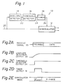
- a prior art system is shown and generally designated by the reference numeral 10.
- the system 10 comprises a demodulator 12, an envelope detector 14, a threshold detector 16, and a timer 18.
- a receive signal 20 which is applied to the system 10 has a format as shown in Fig. 2A.
- Output signals 22, 24 and 26 of the envelope detector 14, threshold detector 16 and timer 18, respectively, have waveforms as shown in Figs. 2B, 2C and 2D.
- the demodulator 12 is selectively operable in different modes as shown in Fig. 2E. As shown in Figs.
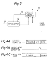
- FIG. 3 Another prior art system is shown in Fig. 3.
- the system generally 30, comprises a demodulator 32 and a unique word detector 34.
- a receive signal 36 which enters the system 30 has a format as shown in Fig. 4A.
- the output signal 38 of the unique word detector 34 is shown in Fig. 4B, and the operation modes of the demodulator 32 are shown in Fig. 4C. It will be seen that in this particular prior art system 30 on detection of a unique word the operation mode of the demodulator 32 is switched from a two-phase to a four-phase PSK mode.
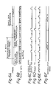
- a modulator/demodulator operation mode control system of the present invention is shown in Fig. 5 and signals appearing therein, in Figs. 6A-6F.
- the system generally 40, comprises a demodulator 42, a unique word detector 44, a receive frame synchronizing circuit 46, a switchover detector 48, a mode decision circuit 50, an AND gate 52, D-type flop-flops 54, 56 and 58, and Exclusive-OR gates 60 and 62.
- One output 64 of the demodulator 42 is applied to one input terminal of the unique word detector 44 and the Exclusive-OR gate 62, while the other output 66 is applied to the receive frame synchronizing circuit 46 and the other input terminal of the unique word detector 44.
- the demodulator output 66 is routed to a digital section as a clock.
- One output 68 of the unique word detector 44 is fed to the D flip-flop 56 and the AND gate 52, while the other output 70 is fed to the Exclusive-OR gate 60 and a D-terminal of the flip-flop 54.
- the output 72 of the AND gate 52 is coupled to the receive frame synchronizing circuit 46.
- One output 74 of the circuit 46 in turn is routed to the AND gate 52, a C-terminal of the D flip-flop 54, the mode decision circuit 50 and the switchover detector 48, while being delivered to the digital section as a frame output.
- the output of the D flip-flop 54 is applied to the Exclusive-OR gate 60 and the Exclusive-OR gate 62 which is adapted to apply data to the digital section.
- the other output 78 of the receive frame synchronizing circuit 46 is fed to the mode decision circuit 50, the D flip-flops 56 and 58, and the switchover detector 48,
- the output 80 of the Exclusive OR gate 60 is coupled to a D-terminal of the D flip-flop 58.
- the output 82 of the D flip-flop 56 is inputted to the mode decision circuit 50 as an output 84 of the switchover detector 48. Further, the output 86 of the D flip-flop 58 is fed back to the demodulator 42 by way of the mode decision circuit 50.
- a switchover signal is implemented with an F -bit signal which is a sequence of K unique words, each of which has L bits. It will be noted that if K ⁇ L ( F the switchover signal will be fully transmitted within one frame but, if otherwise, the switchover signal will occupy a plurality of frames.
- the system 40 shown in Fig. 5 is assumed to use a synchronous detection type demodulator.
- unique word UW o is detected responsive to a "frame pulse" 74 which is outputted by the receive frame synchronizing circuit 46, thereby providing an "ambiguity remove signal” 76.
- the Exclusive-OR gate 60 to which the signal 76 is applied produces a unique pattern polarity signal 80 which is free from “ambiguity”.
- the signal 80 is discriminated responsive to an "aperture pulse” 78 and then applied to the mode decision circuit 50.
- a "unique word detection signal” (not dependent upon polarity) 68 is also discriminated responsive to an aperture pulse 78 and then fed to the switchover detector 48.
- the switchover detector 48 determines that a switchover signal frame has been received when, of the K unique words expected to arrive in the case of a switchover signal, more than a predetermined number (e. g. T ) of unique words have occurred.
- the mode decision circuit 50 decodes a mode instruction signal and then generates a "demodulator mode control signal" 88 to start controlling the demodulator 42 in a new mode at a predetermined timing.
- the system 40 having the above construction will be operated as follows.
- a transmit station When changing the operation mode is decided, a transmit station subjects a plurality ( K ) of unique words UW, UW1, UW2, . . . , UW k , which are to be transmitted after a synchronizing unique word (UW o in this particular embodiment) that appears for each frame, to "polarity modulation" in order to send K -bit binary data which designates a modulation mode to hold next. Simultaneously, the transmit station switches over the transmission mode at the beginning of the next frame or at any other predetermined timing.
- a receive station samples and stores presence of unique words as well as polarity detection signals responsive to a timing signal, which is supplied thereto from the receive frame synchronizing circuit 46.
- the receive station determines that a switchover signal has been received. then decodes the binary code as represented by the stored polarity detection signals to thereby select an operation mode of the demodulator 42 which is to hold next, and then switches the demodulator mode at the beginning of the next frame or at any other predetermined timing.
- the system 40 is capable of surely changing the operation mode even when the SN ratio is poor. Specifically, concerning the detection of a unique word itself (assumed to have a length of L bits) , there are provided L bits which is long enough to be detected even under poor SN ratio conditions, a word having high self-correlation, and an allowable number of error bits (with a threshold value ⁇ ), so that the unique word detection error rate is sufficiently lower than the bit error rate. Even though the number of bit errors in the unique word may exceed the threshold value to such an extent that a unique word is overlooked, the probability of falling to correctly decide polarity (decision by majority of L /2) is negligible.
- the sampling which uses aperture pulses as previously stated is effective to substantially exclude erroneous detection pulses which may appear even during steady operation due to accidental coincidence between an L -bit signal included in random transmit signals and the unique word.
- the code length K which is an important constant in switchover detection and an allowable number of overlooks, it is possible to suppress the probability of malfunction of the system due to detection error to a practically negligible degree.
- a modulator/demodulator furnished with numerous operation modes is surely operable even under poor SN ratio conditions without the need for order wires and whenever desired and in any desired mode.
- This offers users who use various different signal modes high-speed and highly reliable signal transmission services by setting up an optimum operation mode, i. e. , a combination of data rate, modulation system, error-correcting coding rate and others which is most effective for given transmission conditions.
- the present invention allows a versatile, flexible and high-performance satellite communication link to be set up which is extensively applicable to bussiness communication and mobile communication.
Landscapes
- Engineering & Computer Science (AREA)
- Signal Processing (AREA)
- Computer Networks & Wireless Communication (AREA)
- Quality & Reliability (AREA)
- Digital Transmission Methods That Use Modulated Carrier Waves (AREA)
- Synchronisation In Digital Transmission Systems (AREA)
- Communication Control (AREA)
- Radio Relay Systems (AREA)
Claims (2)
- System zur Steuerung der Betriebsweise eines Modulators/Demodulators, das die Betriebsweise des Modulators/Demodulators umschaltet, dadurch gekennzeichnet, daß eine Sendestation, wenn ihre Betriebsweise von einer zur anderen umgeschaltet wird, geeignet ist, mehrere (K) einzigartige Wörter zu erzeugen nach einem einzigartigen Wort für eine Synchronisation, das für jeden Rahmen übertragen wird, und dann Polaritäten der K-einzigartigen Wörter moduliert zum Senden von K-Bits binären Daten und dadurch Bezeichnen einer Betriebsweise, die als nächstes gehalten werden soll, und eine Empfangsstation geeignet ist zum Unterscheiden eines Umschaltens, wenn mehr als eine bestimmte Anzahl von einzigartigen Wörtern innerhalb einer bestimmten Zeitdauer empfangen worden sind und die auf den K-Bits binären Daten basierende Betriebsweise identifiziert, wobei das Umschalten abhängig ist von einer bestimmten Kombination aus Modulationssystem, Fehlerkorrekturcodiersystem und Datenübertragungsrate.
- Verfahren zur Steuerung der Betriebsweise eines Modulators/Demodulators, der die Betriebsweise des Modulators/Demodulators umschaltet, gekennzeichnet durch Erzeugen an einer Sendestation, wenn die Betriebsweise von einer zur anderen umgeschaltet wird, von mehreren (K) einzigartigen Wörtern nach einem einzigartigen Wort für eine Synchronisation, das für jeden Rahmen übertragen wird, anschließend Modulieren von Polaritäten der K-einzigartigen Wörter, und Senden von K-Bits binären Daten, wodurch eine Betriebsweise bestimmt wird, die als nächstes gehalten wird, und Unterscheiden an einer Empfangsstation eines Umschaltens, wenn mehr als eine bestimmte Anzahl von einzigartigen Wörtern innerhalb einer bestimmten Zeitdauer empfangen worden sind, und Identifizieren der Modulationsweise auf der Basis der K-Bits binären Daten, wobei das Umschalten abhängig ist von einer bestimmten Kombination aus Modulationssystem, Fehlerkorrekturcodiersystem und Datenübertragungsrate.
Applications Claiming Priority (2)
| Application Number | Priority Date | Filing Date | Title |
|---|---|---|---|
| JP60075131A JPH0654923B2 (ja) | 1985-04-09 | 1985-04-09 | 変復調装置の動作制御方式 |
| JP75131/85 | 1985-04-09 |
Publications (3)
| Publication Number | Publication Date |
|---|---|
| EP0197541A2 EP0197541A2 (de) | 1986-10-15 |
| EP0197541A3 EP0197541A3 (en) | 1988-09-21 |
| EP0197541B1 true EP0197541B1 (de) | 1992-01-22 |
Family
ID=13567330
Family Applications (1)
| Application Number | Title | Priority Date | Filing Date |
|---|---|---|---|
| EP86104775A Expired EP0197541B1 (de) | 1985-04-09 | 1986-04-08 | System zur Steuerung der Arbeitsweise eines Modulators/Demodulators |
Country Status (6)
| Country | Link |
|---|---|
| US (1) | US4833696A (de) |
| EP (1) | EP0197541B1 (de) |
| JP (1) | JPH0654923B2 (de) |
| AU (1) | AU586858B2 (de) |
| CA (1) | CA1267703A (de) |
| DE (1) | DE3683522D1 (de) |
Families Citing this family (19)
| Publication number | Priority date | Publication date | Assignee | Title |
|---|---|---|---|---|
| US5054034A (en) * | 1985-05-20 | 1991-10-01 | Telebit Corporation | Ensemble modem structure for imperfect transmission media |
| US4852122A (en) * | 1987-08-31 | 1989-07-25 | Universal Data Systems, Inc. | Modem suited for wireless communication channel use |
| US4891806A (en) * | 1987-09-18 | 1990-01-02 | Racal Data Communications Inc. | Constellation multiplexed inband secondary channel for voiceband modem |
| JPH0817428B2 (ja) * | 1988-11-22 | 1996-02-21 | 株式会社日立製作所 | 変復調装置 |
| EP0385042A1 (de) * | 1989-02-28 | 1990-09-05 | International Business Machines Corporation | Verfahren zur Abstimmung des Übertragungsendes in einem Modem |
| EP0389165B1 (de) * | 1989-03-21 | 1996-06-12 | Minnesota Mining And Manufacturing Company | Lichtwellenleiter-Datenverbindungssystem |
| JP3077881B2 (ja) * | 1995-03-07 | 2000-08-21 | 日本電気株式会社 | 復調方法及び復調装置 |
| US5974106A (en) * | 1995-09-01 | 1999-10-26 | Motorola, Inc. | Method and apparatus for multirate data communications |
| US6068933A (en) | 1996-02-15 | 2000-05-30 | American National Can Company | Thermoformable multilayer polymeric film |
| JPH10322407A (ja) * | 1997-05-16 | 1998-12-04 | Matsushita Electric Ind Co Ltd | デュアルバンドデータ通信装置 |
| US6426959B1 (en) | 1998-01-20 | 2002-07-30 | Innovative Communications Technologies, Inc. | System and method for facilitating component management in a multiple vendor satellite communications network |
| US6381250B1 (en) | 1998-01-23 | 2002-04-30 | Innovative Communications Technologies, Inc. | Capacity allocation system using semi-autonomous network elements to implement and control a transmission schedule |
| US6567475B1 (en) * | 1998-12-29 | 2003-05-20 | Ericsson Inc. | Method and system for the transmission, reception and processing of 4-level and 8-level signaling symbols |
| IL130540A (en) * | 1999-06-17 | 2003-07-31 | Tadiran Telecom Business Syste | System having a port with two operating modes |
| JP4517430B2 (ja) * | 2000-01-24 | 2010-08-04 | ソニー株式会社 | 無線伝送方法 |
| US8106813B2 (en) * | 2010-01-27 | 2012-01-31 | Unnikrishna Sreedharan Pillai | Multichannel constant envelope orthogonal waveforms using receiver design |
| JP5877388B2 (ja) | 2010-12-20 | 2016-03-08 | パナソニックIpマネジメント株式会社 | 通信装置、通信方法、端末装置、及び、通信システム |
| BE1021568B1 (fr) | 2013-03-11 | 2015-12-14 | N.G.M. Sprl | Tricycle |
| JP7512153B2 (ja) * | 2020-09-28 | 2024-07-08 | ニデックインスツルメンツ株式会社 | エンコーダ、およびエンコーダの通信制御方法 |
Family Cites Families (12)
| Publication number | Priority date | Publication date | Assignee | Title |
|---|---|---|---|---|
| US3688197A (en) * | 1965-10-21 | 1972-08-29 | Kahn Res Lab | Communication system with selection means for determining the modulation mode of a received signal |
| JPS49131610A (de) * | 1973-04-22 | 1974-12-17 | ||
| US4055808A (en) * | 1976-05-20 | 1977-10-25 | Intertel, Inc. | Data communications network testing system |
| US4128809A (en) * | 1976-08-31 | 1978-12-05 | Nippon Electric Co., Ltd. | Time diversity receiver for processing repeatedly received signal bits in consideration of a maximum-level and/or a favorably received signal bit |
| DE2641782A1 (de) * | 1976-09-17 | 1978-03-23 | Licentia Gmbh | Schaltungsanordnung fuer die digitale frequenzanzeige des am- und fm-bereiches in einem rundfunkgeraet |
| US4156867A (en) * | 1977-09-06 | 1979-05-29 | Motorola, Inc. | Data communication system with random and burst error protection and correction |
| US4387440A (en) * | 1980-03-03 | 1983-06-07 | Eaton Michael D | Modem control device code multiplexing |
| FR2503965B1 (fr) * | 1981-04-08 | 1987-07-24 | Thomson Csf | Procede de protection contre les erreurs de transmission des messages radio-telegraphiques et dispositif de mise en oeuvre |
| US4549302A (en) * | 1981-06-15 | 1985-10-22 | Hayes Microcomputer Products, Inc. | Modem with improved escape sequence mechanism to prevent escape in response to random occurrence of escape character in transmitted data |
| US4481489A (en) * | 1981-07-02 | 1984-11-06 | Motorola Inc. | Binary signal modulating circuitry for frequency modulated transmitters |
| US4620294A (en) * | 1983-09-09 | 1986-10-28 | Cts Corporation | Digital signal processor modem |
| US4756007A (en) * | 1984-03-08 | 1988-07-05 | Codex Corporation | Adaptive communication rate modem |
-
1985
- 1985-04-09 JP JP60075131A patent/JPH0654923B2/ja not_active Expired - Lifetime
-
1986
- 1986-04-02 US US06/847,366 patent/US4833696A/en not_active Expired - Fee Related
- 1986-04-07 AU AU55697/86A patent/AU586858B2/en not_active Ceased
- 1986-04-08 EP EP86104775A patent/EP0197541B1/de not_active Expired
- 1986-04-08 DE DE8686104775T patent/DE3683522D1/de not_active Expired - Lifetime
- 1986-04-08 CA CA000506054A patent/CA1267703A/en not_active Expired
Also Published As
| Publication number | Publication date |
|---|---|
| US4833696A (en) | 1989-05-23 |
| AU586858B2 (en) | 1989-07-27 |
| EP0197541A2 (de) | 1986-10-15 |
| EP0197541A3 (en) | 1988-09-21 |
| CA1267703A (en) | 1990-04-10 |
| AU5569786A (en) | 1986-10-16 |
| JPH0654923B2 (ja) | 1994-07-20 |
| JPS61234154A (ja) | 1986-10-18 |
| DE3683522D1 (de) | 1992-03-05 |
Similar Documents
| Publication | Publication Date | Title |
|---|---|---|
| EP0197541B1 (de) | System zur Steuerung der Arbeitsweise eines Modulators/Demodulators | |
| US4688210A (en) | Method of and arrangement for synchronizing the receiver arrangements in a digital multiplex transmission system | |
| AU672700B2 (en) | Method and apparatus for establishing and maintaining frame synchronization in a satellite communication system | |
| US4639937A (en) | HF avalanche relay communication technique | |
| US4099121A (en) | Spatial diversity satellite communications system with error control | |
| EP0125805B1 (de) | Bit-Fehler Detektionsschaltung für eine PSK-modulierte Trägerwelle | |
| US4232197A (en) | Processor for a TDMA burst modem | |
| US4107608A (en) | Method and apparatus for burst synchronization in a time division multiple access communication system | |
| US4723310A (en) | Digital data transmission system by coherent light wave modulation | |
| KR20000005381A (ko) | Tdm/tdma 시스템에서 비트 동기화 및 에러 검출을 함께 수행하기 위한 방법 | |
| US6452914B2 (en) | Mobile TDMA/GSM system which uses a plurality of bits for the steal symbols/flags | |
| US4663768A (en) | Diversity system of selection type equipped with a code correction/switch circuit for receiving a PSK or QAM wave carrying differentially encoded signal | |
| US3777062A (en) | Transmission system for a time-divisional multiplex psk signal | |
| CZ285354B6 (cs) | Způsob synchronizace vzorkového signálu hodin s přijímaným datovým signálem a zařízení ke provádění tohoto způsobu | |
| KR100442926B1 (ko) | 데이터 인코딩 방법 및 장치와 인코딩 데이터 신호의 디코딩 방법 및 장치 | |
| EP0315377A2 (de) | LORAN-C-Navigationssystem | |
| US4414662A (en) | System for the transmission of digital data in packets | |
| US5285458A (en) | System for suppressing spread of error generated in differential coding | |
| US4213007A (en) | Method and apparatus for monitoring a pulse-code modulated data transmission | |
| US5654989A (en) | Method and apparatus for symbol timing tracking | |
| US7095818B2 (en) | Data transmission process with auto-synchronized correcting code, auto-synchronized coder and decoder, corresponding transmitter and receiver | |
| JPH0225306B2 (de) | ||
| US4426711A (en) | Process for the transmission of service signals for a digital radio beam, as well as transmitter and receiver for using such a process | |
| Ryan | Optimal signaling for meteor burst channels | |
| JPH06101718B2 (ja) | Tdmaフレ−ム同期方法 |
Legal Events
| Date | Code | Title | Description |
|---|---|---|---|
| PUAI | Public reference made under article 153(3) epc to a published international application that has entered the european phase |
Free format text: ORIGINAL CODE: 0009012 |
|
| 17P | Request for examination filed |
Effective date: 19860408 |
|
| AK | Designated contracting states |
Kind code of ref document: A2 Designated state(s): DE FR GB NL |
|
| PUAL | Search report despatched |
Free format text: ORIGINAL CODE: 0009013 |
|
| AK | Designated contracting states |
Kind code of ref document: A3 Designated state(s): DE FR GB NL |
|
| 17Q | First examination report despatched |
Effective date: 19900808 |
|
| GRAA | (expected) grant |
Free format text: ORIGINAL CODE: 0009210 |
|
| AK | Designated contracting states |
Kind code of ref document: B1 Designated state(s): DE FR GB NL |
|
| REF | Corresponds to: |
Ref document number: 3683522 Country of ref document: DE Date of ref document: 19920305 |
|
| ET | Fr: translation filed | ||
| PLBE | No opposition filed within time limit |
Free format text: ORIGINAL CODE: 0009261 |
|
| STAA | Information on the status of an ep patent application or granted ep patent |
Free format text: STATUS: NO OPPOSITION FILED WITHIN TIME LIMIT |
|
| 26N | No opposition filed | ||
| PGFP | Annual fee paid to national office [announced via postgrant information from national office to epo] |
Ref country code: GB Payment date: 19960403 Year of fee payment: 11 |
|
| PGFP | Annual fee paid to national office [announced via postgrant information from national office to epo] |
Ref country code: FR Payment date: 19960423 Year of fee payment: 11 |
|
| PGFP | Annual fee paid to national office [announced via postgrant information from national office to epo] |
Ref country code: NL Payment date: 19960430 Year of fee payment: 11 |
|
| PGFP | Annual fee paid to national office [announced via postgrant information from national office to epo] |
Ref country code: DE Payment date: 19960627 Year of fee payment: 11 |
|
| PG25 | Lapsed in a contracting state [announced via postgrant information from national office to epo] |
Ref country code: GB Effective date: 19970408 |
|
| PG25 | Lapsed in a contracting state [announced via postgrant information from national office to epo] |
Ref country code: NL Effective date: 19971101 |
|
| GBPC | Gb: european patent ceased through non-payment of renewal fee |
Effective date: 19970408 |
|
| PG25 | Lapsed in a contracting state [announced via postgrant information from national office to epo] |
Ref country code: FR Free format text: LAPSE BECAUSE OF NON-PAYMENT OF DUE FEES Effective date: 19971231 |
|
| PG25 | Lapsed in a contracting state [announced via postgrant information from national office to epo] |
Ref country code: DE Free format text: LAPSE BECAUSE OF NON-PAYMENT OF DUE FEES Effective date: 19980101 |
|
| NLV4 | Nl: lapsed or anulled due to non-payment of the annual fee |
Effective date: 19971101 |
|
| REG | Reference to a national code |
Ref country code: FR Ref legal event code: ST |