EP0158618A2 - Elektrischer Klinkenstecker - Google Patents
Elektrischer Klinkenstecker Download PDFInfo
- Publication number
- EP0158618A2 EP0158618A2 EP85850121A EP85850121A EP0158618A2 EP 0158618 A2 EP0158618 A2 EP 0158618A2 EP 85850121 A EP85850121 A EP 85850121A EP 85850121 A EP85850121 A EP 85850121A EP 0158618 A2 EP0158618 A2 EP 0158618A2
- Authority
- EP
- European Patent Office
- Prior art keywords
- spring
- jack
- switching
- circuit board
- housing
- Prior art date
- Legal status (The legal status is an assumption and is not a legal conclusion. Google has not performed a legal analysis and makes no representation as to the accuracy of the status listed.)
- Withdrawn
Links
- 230000014759 maintenance of location Effects 0.000 claims abstract description 5
- 239000004020 conductor Substances 0.000 claims description 8
- 238000003780 insertion Methods 0.000 claims description 6
- 230000037431 insertion Effects 0.000 claims description 6
- 238000005452 bending Methods 0.000 claims description 5
- 230000013011 mating Effects 0.000 claims description 3
- 230000000630 rising effect Effects 0.000 claims description 2
- 230000007246 mechanism Effects 0.000 abstract description 29
- 239000000428 dust Substances 0.000 abstract description 5
- 230000007613 environmental effect Effects 0.000 abstract description 3
- 239000000356 contaminant Substances 0.000 abstract description 2
- 230000008901 benefit Effects 0.000 description 8
- 230000009471 action Effects 0.000 description 5
- 239000000463 material Substances 0.000 description 3
- 238000004140 cleaning Methods 0.000 description 2
- BASFCYQUMIYNBI-UHFFFAOYSA-N platinum Chemical compound [Pt] BASFCYQUMIYNBI-UHFFFAOYSA-N 0.000 description 2
- 229910001316 Ag alloy Inorganic materials 0.000 description 1
- 229910001020 Au alloy Inorganic materials 0.000 description 1
- 229910001260 Pt alloy Inorganic materials 0.000 description 1
- 230000001627 detrimental effect Effects 0.000 description 1
- 239000012530 fluid Substances 0.000 description 1
- PCHJSUWPFVWCPO-UHFFFAOYSA-N gold Chemical compound [Au] PCHJSUWPFVWCPO-UHFFFAOYSA-N 0.000 description 1
- 239000010931 gold Substances 0.000 description 1
- 238000004519 manufacturing process Methods 0.000 description 1
- 230000004044 response Effects 0.000 description 1
- 230000000717 retained effect Effects 0.000 description 1
- 230000001953 sensory effect Effects 0.000 description 1
- 238000000926 separation method Methods 0.000 description 1
- 229910000679 solder Inorganic materials 0.000 description 1
- 239000007787 solid Substances 0.000 description 1
Images


Classifications
-
- H—ELECTRICITY
- H01—ELECTRIC ELEMENTS
- H01R—ELECTRICALLY-CONDUCTIVE CONNECTIONS; STRUCTURAL ASSOCIATIONS OF A PLURALITY OF MUTUALLY-INSULATED ELECTRICAL CONNECTING ELEMENTS; COUPLING DEVICES; CURRENT COLLECTORS
- H01R24/00—Two-part coupling devices, or either of their cooperating parts, characterised by their overall structure
- H01R24/58—Contacts spaced along longitudinal axis of engagement
-
- H—ELECTRICITY
- H01—ELECTRIC ELEMENTS
- H01R—ELECTRICALLY-CONDUCTIVE CONNECTIONS; STRUCTURAL ASSOCIATIONS OF A PLURALITY OF MUTUALLY-INSULATED ELECTRICAL CONNECTING ELEMENTS; COUPLING DEVICES; CURRENT COLLECTORS
- H01R12/00—Structural associations of a plurality of mutually-insulated electrical connecting elements, specially adapted for printed circuits, e.g. printed circuit boards [PCB], flat or ribbon cables, or like generally planar structures, e.g. terminal strips, terminal blocks; Coupling devices specially adapted for printed circuits, flat or ribbon cables, or like generally planar structures; Terminals specially adapted for contact with, or insertion into, printed circuits, flat or ribbon cables, or like generally planar structures
- H01R12/70—Coupling devices
- H01R12/71—Coupling devices for rigid printing circuits or like structures
- H01R12/712—Coupling devices for rigid printing circuits or like structures co-operating with the surface of the printed circuit or with a coupling device exclusively provided on the surface of the printed circuit
- H01R12/716—Coupling device provided on the PCB
-
- H—ELECTRICITY
- H01—ELECTRIC ELEMENTS
- H01R—ELECTRICALLY-CONDUCTIVE CONNECTIONS; STRUCTURAL ASSOCIATIONS OF A PLURALITY OF MUTUALLY-INSULATED ELECTRICAL CONNECTING ELEMENTS; COUPLING DEVICES; CURRENT COLLECTORS
- H01R13/00—Details of coupling devices of the kinds covered by groups H01R12/70 or H01R24/00 - H01R33/00
- H01R13/46—Bases; Cases
- H01R13/52—Dustproof, splashproof, drip-proof, waterproof, or flameproof cases
-
- H—ELECTRICITY
- H01—ELECTRIC ELEMENTS
- H01R—ELECTRICALLY-CONDUCTIVE CONNECTIONS; STRUCTURAL ASSOCIATIONS OF A PLURALITY OF MUTUALLY-INSULATED ELECTRICAL CONNECTING ELEMENTS; COUPLING DEVICES; CURRENT COLLECTORS
- H01R13/00—Details of coupling devices of the kinds covered by groups H01R12/70 or H01R24/00 - H01R33/00
- H01R13/66—Structural association with built-in electrical component
- H01R13/70—Structural association with built-in electrical component with built-in switch
- H01R13/703—Structural association with built-in electrical component with built-in switch operated by engagement or disengagement of coupling parts, e.g. dual-continuity coupling part
-
- H—ELECTRICITY
- H01—ELECTRIC ELEMENTS
- H01R—ELECTRICALLY-CONDUCTIVE CONNECTIONS; STRUCTURAL ASSOCIATIONS OF A PLURALITY OF MUTUALLY-INSULATED ELECTRICAL CONNECTING ELEMENTS; COUPLING DEVICES; CURRENT COLLECTORS
- H01R2107/00—Four or more poles
Definitions
- the present invention is directed to an electrical jack and, more particularly, to a jack for use on circuit boards to provide electrical continuity between conductive paths on the circuit board and plugs inserted into the jack.
- Electrical jacks for mounting on a printed circuit board are known in the prior art. There are jacks which have contact elements parallel with the axis of a mounted plug. There are also jacks having at least the lug portions of contact elements perpendicular to the axis of a mounted plug. Furthermore, there are jacks of both types designed for receiving multiple plugs. Known multiple plug jacks, however, require side-by-side plug insertion, generally due to the structure of the contact springs. Consequently, known multiple plug jacks tend to occupy a relatively large space on a circuit board.
- the present invention is directed to a jack which occupies a relatively small space on a circuit board by having vertically stacked receiving passages for multiple plugs.
- the jack includes a non-conductive housing having a center plane which is substantially perpendicular to the bottom wall of the jack. As indicated, the jack includes a plurality of receiving mechanisms for plugs. The receiving mechanisms are stacked along the center plane.
- the jack has spring mechanisms for providing continuity between conductive paths on the circuit board and the plugs, as well as mechanisms for fastening the springs to the housing.
- one embodiment of the present invention includes a housing having a base and front and rear structures rising from the base.
- the front structure includes upper and lower passages for receiving upper and lower plugs.
- At one side of the front structure there are facing grooves forming a pocket for a common sleeve spring having upper and lower spring elements for contacting the sleeves of the upper and lower plugs.
- the sleeve spring usually provides a common ground element for both plugs.
- the jack also includes first and second switch mechanisms for both the upper and lower plugs. The first and second switch mechanisms are functioned by the lower plug and are located on a first side of the center plane, while the third and fourth switch mechanisms are functioned by the upper plug and are located on a second side of the center plane.
- a cover having fastening mechanisms at both the front and rear of the housing shields the switch mechanisms from dust and other detrimental environmental factors.
- the present jack is particularly important because of its compact profile which includes vertically-stacked plugs.
- the compact profile is possible because of the advantageous relationship of the common sleeve spring and a pair of switching mechanisms on each side of the center plane of the housing with one pair being operable by contact portions located below a contact plane on which all switching contactors are substantially centered, while the other pair has contact portions located above the common contactor plane.
- the dust cover may be positively locked to the housing by using a block and loop lock mechanism at the rear of the housing.
- the springs used for the switching mechanisms for the upper plug have length so that cantilever spring action provides sufficient contact force between the contactors of the springs of a switching mechanism or between a spring and a plug.
- the present invention solves the problem of providing an adequate amount of force between the contactors of the springs of the switching mechanisms for the lower plug.
- the contact ring and tip springs for the lower plug not only utilize spring force due to a cantilever design, but also combine a torsional force about an axis orthogonal to the axis about which the cantilever bending occurs.
- the present invention is of still further advantage in that lugs from the springs of the switching mechanisms from one side of the center plane may be paired with lugs of the switching mechanisms from the other side of the center plane to provide lug pairs for retaining the jack to the circuit board.
- the retention pairs are advantageously shaped to provide a sensory response to the person inserting the jack into the hole pattern so that he knows when the jack has been received by the circuit board.
- the lug shape provides for a lesser force during insertion than for removal so the jack is relatively easy to insert, but somewhat more difficult to remove.
- the present jack provides a compact device for connecting plugs to a printed circuit board. This important feature has resulted in a large number of advantages as indicated briefly hereinbefore. These advantages and other objects obtained by the present invention are further explained and may be better understood by reference to the sketches and descriptive matter hereinafter. A preferred embodiment of the invention is shown and described. It is understood, however, that the embodiment is exemplary and that the invention may be practiced to the full extent of the general meaning of the terms of the appended claims.
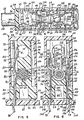
- Jack 10 includes housing 12 having upper receiving passage 14 and lower receiving passage 16 for a plug as shown at 18.
- Jack 10 further includes sleeve spring 20, used generally as an electrical ground, and first, second, third and fourth switching mechanisms 22, 24, 26 and 28.
- Cover 30 protects the electrical elements from dust and other environmental contaminants.
- Housing 12 is made from a non-conducting material and includes a base portion 32 from which a forward structure 34 and a rear structure 36 rises.
- Base 32 has a wider, lower portion 38 and a narrower, upper portion 40.
- Upper portion 40 is formed with a semi-cylindrical top side for cradling the lower plug.
- a plurality of slots 82 are located in lower portion 38 slightly outwardly from each side of upper portion 40. The slots are shaped to receive the mid-portions of the several springs as described hereinafter.
- Standoffs 44 protrude from bottom side 46 near both the forward and rearward ends of housing 12 to hold the bottom side somewhat off circuit board 47 (see FIGURE 2).
- Forward structure 34 includes upper passage 14 and lower passage 16 as indicated hereinbefore. Passages 14 and 16 are cylindrical and have a diameter only slightly greater than the smaller diameter portion 56 of sleeve 52 of plug 18. Passages 14 and 16 are centered on the vertical, center plane of housing 12 which is perpendicular to bottom wall 46. Forward structure 34 has an outer portion 48 which is the same width as lower portion 38 of base 32 and rises approximately the thickness of cover 30 above the inner portion 50 of forward structure 34. Forward structure 34 has sufficient thickness to provide support structure for sleeve spring 20 and normal springs 118 and 126, as well as relatively solid support for upper and lower plugs 18.
- Plug 18 is representative of the type of plug used with jack 10.
- Plug 18 includes sleeve 52 having a shoulder 54 separating an insertable, smaller diameter portion 56 from an uninsertable, greater diameter portion 58. Shoulder 54 butts against front wall 49.
- Sleeve 52 is tubular and contains a smaller diameter tube therewithin, the end of which forms ring 60.
- the tubes of sleeve 52 and ring 60 are separated by a non-conducting material 62.
- Ring 60 has an end portion 64 of greater diameter, which is approximately the same diameter as lesser diameter portion 56 of sleeve 52.
- a cylindrical rod having ball 66 at its end is axially contained within the tube of ring 60.
- the rod of ball 66 is separated from the tube of ring 60 by non-conducting material 68.
- Materials 62 and 68 may be different and separated, but are generally the same material and are connected.
- a neck portion 70 separates ball 66 from non-conducting material 68.
- the ball 66, ring 60, and sleeve 52 portions of plug 18 may be electrically connected to elements of an electrical circuit (not shown).
- Sleeve spring 20 is received in structure just behind outer portion 48 of forward structure 34 along a first side of inner portion 50.
- Sleeve spring 20 is shown most clearly in FIGURES 2 and 5.
- Sleeve spring 20 is made from a flat plate of conducting material.
- Spring 20 includes an upper portion having a frame 72 with upper spring element 74 and lower spring element 76.
- the lower portion of spring 20 includes lug 78 and mid-portion 80 formed for fastening engagement with for- wardmost slot 82 on the first side of the lower portion 38 of base 32 of housing 12.
- Each of spring elements 74 and 76 is centered on strip 20 and is bordered on the top and sides by a slot separating it from frame 72.
- Each of spring elements 74 and 76 is bent inwardly at the connecting line with frame 72.
- each element 74 and 76 is again bent so that its contact portion 84, 86 is approximately parallel with frame 72.
- Contact portions 84 and 86 are formed with a detent in the outer sides so as to shape the inner sides arcuately for contact with sleeve 52.
- Sleeve spring 20 is retained by a pair of spaced-apart, facing grooves 88 forming a pocket in inner portion 50 of housing 12 as shown in FIGURE 3.
- Upper opening 90 and lower opening 92 are provided for contact portions 84 and 86 to extend through to contact a plug 18.
- grooves 88 provide support to counteract the spring force between frame 72 and the particular spring element 74 or 76.
- the outermost side of sleeve spring 20 from the top of forward structure 34 to lower portion 38 of base 32 may be covered by a wall extending between grooves 88 or may be open as shown in FIGURE 3.
- a vertical slot 94 is formed in inner portion 50 of forward structure 34 on the sidewall opposite from sleeve spring 20. Groove 94 is formed to receive the matching tongue 96 (see FIGURE 1) of cover 30.
- Cover 30 has a top 98 with a sidewall 100 having tongue 96 at its forward end and a sidewall 102 opposite therefrom.
- Sidewall 100 also includes a wide slot 104 for receiving mating surface 106 adjacent to groove 94.
- a back wall 108 extends downwardly from top 98 and extends below both sidewalls 100 and 102. At the lower end of back wall 108 there is an opening 110 with essentially a loop 112 of material thereabout.
- a protruding block 114 is located centrally on the backside of lower portion 38 of base 32. Loop 112 and block 114, engage in cooperation with tongue 96 and groove 94 to hold cover 30 to jack 10.
- the first switching mechanism 22 includes lower ring spring 116 and a first normal spring 118.
- the second switching mechanism 24 includes a lower tip spring 120 and a second normal spring 122.
- the third switching mechanism 26 includes an upper ring spring 124 and a third normal spring 126 (see FIGURE 3).
- the fourth switching mechanism 28 includes an upper tip spring 128 and a fourth normal spring 130. Because of the symmetry of the design, second normal spring 122 and third normal spring 126 are identical, while first normal spring 118 and fourth normal spring 130 are identical.
- Each indicated set of normal springs is similar except the lugs 78 and the horizontal portions 140 have bends in directions opposite from the other since on each side of the center plane of jack 10, one normal spring has horizontal portion 140 pointing forwardly, while the other normal spring has horizontal portion 140 pointing rearwardly.
- Normal spring 118 is representative of the other normal springs 122, 126, and 130. As shown in FIGURES 2 and 3, normal spring 118 is a flat strip of conducting material and includes a lug 78, a vertical portion 134 with a mid-portion 80 for fastening spring 118 to base 38 therebetween. Lug 78 and fastening mid-portion 80 are discussed in more detail hereinafter. Vertical portion 134 extends upwardly to approximately the lower edge of upper passage 14 of housing 12. Vertical portion 134 is in contact with and is supported by the flat surface or by ridges or other standoff shapes on sidewall 138 of forward structure 34 of housing ' 12. In like fashion, the vertical portions of the other normal springs are also supported appropriately by sidewalls of either rear structure 36 or forward structure 34.
- Horizontal portion 140 extends away from vertical portion 134 toward the appropriate mating spring, in this case, lower ring spring 116. Horizontal portion 140 is bent inwardly and again outwardly so that the end part of horizontal portion 140 is located inwardly from, but essentially parallel to, the flat surface of the supported vertical portion 134.
- a contact 142 made from, for example, a gold, platinum, and silver alloy is attached to the outer surface near the end of horizontal portion 140.
- lower ring spring 116 and lower tip spring 120 are similarly configured except each faces in opposite directions from the other so that bends in each are opposite from the other. Nevertheless, ring spring 116 is hereinafter described and is also representative of the structure of tip spring 120.
- lower ring spring 116 is a flat strip of conducting material and includes a lug 78 extending below mid-portion 80 which includes mechanism for fastening spring 116 to base 32 as described hereinafter.
- Cantilever portion 148 rises above mid-portion 80 to a connect portion 150 beneath which contact portion 152 extends downwardly.
- Cantilever portion 148 is connected to mid-portion 80 symmetrically with respect to a centerline bisecting lug 78 and mid-portion 80.
- cantilever portion 148 is shaped so as to incline toward normal spring 118 before inclining again vertically parallel to the center line of spring 116.
- Connect portion 150 extends horizontally in a direction away from normal spring l18.
- Connect portion 150 connects cantilever portion 148 with contact portion 152.
- the upper edge of connect portion 150 is approximately the same height as the upper end of vertical portion 134 of normal spring 118.
- Contact portion 152 extends downwardly not quite half the distance from connect portion 150 to mid-portion 80.
- Cantilever portion 148 is inclined sufficiently toward normal spring l18 so that the outer edges of the upper portion of cantilever portion 148 and contact portion 152 are approximately in line with the outermost edges of mid-portion 80.
- Lower ring spring 116 provides a spring force between contactor 142 of normal spring 118 and contactor 154, which is attached to connecting portion 150 in an orientation preferably perpendicular to contactor 142.
- Lower ring spring 116 also provides a spring force between contact portion 152 and ring 60 of plug 18 when plug 18 is inserted in lower passage 16.
- cantilever portion 148 Near its upper end, cantilever portion 148 is bent inwardly and again outwardly, e.g. at 156 and 158, so that connecting portion 150 is approximately parallel with but inward from cantilever portion 148.
- Connect portion 150 is located sufficiently inwardly so as to provide a small force between contactors 142 and 154. That is, horizontal portion 140 of normal spring 118 is forced slightly inwardly by the cantilever spring action and also to some extent by torsional force about a vertical axis as discussed more hereinafter.
- Contact portion 152 extends further inwardly from connect portion 150 with bends at 160 and 162.
- the lower part of contact portion 152 is inclined somewhat with respect to the plane of mid-portion 80, but on contact with sleeve 60 of plug 18 is approximately parallel with mid-portion 80.
- contact portion 152 is formed with a detent in its outer side so as to shape the inner side arcuately for better contact with ring 60.
- contact by mid-portion 80, with ring 60 causes a springing action both by cantilever portion 148 with respect to mid-portion 146, i.e., about a horizontal axis, and by contact portion 152 with respect to cantilever portion 148, i.e., about a vertical axis.
- the combined spring force provides more force than would otherwise be available due to simply a cantilever action and provides sufficient force to essentially eliminate contact bounce or other problems associated with contacts when insufficient force exists between the contacts.
- a further advantage results from the present configuration.
- lower tip spring 120 is configured similar to lower ring spring 116 and functions in a similar fashion with respect to normal spring 122 and the ball 66 of a lower plug 18.
- Upper ring spring 124 and upper tip spring 128 are shaped somewhat differently than each other, but, as shown in FIGURE 6, essentially include a lug 78 connected by a mid-portion 80 to a cantilever portion 168.
- a contactor 170 is fastened to cantilever portion 168 approximately centered on the contactor plane.
- Cantilever portion 168 extends above the contactor plane and includes an arcuately shaped end 172 for contacting plug 18.
- each of the cantilevered portions of the upper and lower ring and tip springs is enhanced with an indented groove on the outer side with a corresponding protruding groove on the inner side as shown, for example, at 174 of lower sleeve spring 116.
- Mid-portion 80 and the lugs 78 are substantially the same for the several springs.
- Mid-portion 80 of lower ring spring 116 is typical.
- Mid-portion 80 includes two triangular detents 176 with corresponding protuberances. Each detent 176 has an apex angle pointing upwardly or in the general direction of contactor 154.
- the protruded portion provides a friction fit between the inner and outer walls of slot 82.
- Mid-portion 80 also includes two pair of spaced apart, parallel edges 180, 182, for fitting tightly against the edges of slot 82. Edges 180 are nearest cantilever portion 148 and have the wider separation. Edges 182 are nearest lug 78 and fit within a narrower portion 184 of slot 82.
- At least one lug 78 near the forward end and one lug 78 near the rearward end on each side of the center plane of jack 10 are shaped as shown in FIGURE 6. All of the lugs on one side of this center plane may be shaped identically, while all the lugs on the other side of the center plane may also be shaped identically but with bends in opposite directions from those on the first side of the center plane. It is only necessary that the forward pair and rearward pair be along lines substantially perpendicular to the center plane of the housing so as to form mechanical retention pairs as described hereinafter.
- Lug 164 is bowed outwardly between the bottom wall 46 of housing 12 and end 186.
- lug 164 is bent outwardly at line 188 which is slightly above the bottom 190 of circuit board 47. Somewhat below the likely location of bottom 190 of circuit board 47, lug 164 is bent inwardly, such as at line 192. Preferably, the outward incline of lug 164 between 188 and 192 is greater than the inward incline between 192 and 186 as compared to the plane of mid-portion 80.
- Lug 164 and the lug identified by numeral 144 are directly opposite from one another and form a-retention pair. Since both lugs are bowed outwardly from the center plane of jack 10, each contacts the lower outer edge of the openings 194 in the circuit board so as to hold the jack to the circuit board. More particularly, the lugs apply a small spring force against the lower portion of the circuit board to pull standoffs 44 against the top of the circuit board.
- the present lug configuration advantageously allows for the jack to be inserted into the circuit board rather easily, but requires greater force to pull the jack from the board. This results from the smaller incline of the lug between 186 and 192 and than between 192 and 188.
- a further advantage of the present configuration is that there is a perceptible feel, and even an auditory result, when jack 10 is inserted into the circuit board as points 192 egress from the circuit board openings.
- the lugs 78 of a jack 10 are inserted into the hole pattern on a circuit board 47.
- the jack 10 is simply pressed against the circuit board so that the lugs from opposite sides of the center plane bend inwardly toward one another before snapping outwardly as points 192 pass through the circuit board.
- the outward snapping not only may be auditory, but results in a pulling of the jack to the board thereby providing a certain feel to the person inserting the jack.
- Each of the various lugs is likely aligned with a circuit path and each is likely soldered to that particular path at the bottom of the board.
- a primary advantage of the retention pairs is to hold the jack firm with respect to the board before and during a mass production flow solder operation.
- Cover 30 is installed over jack 10 by inserting tongue 96 in groove 94 and pressing cover 30 downwardly against housing 12 until loop 112 fits over block 114.
- a lower plug 18 may then be inserted in lower passage 16.
- Ball 66 and ring 60 contact portions 152 of lower ball spring 120 and lower ring spring 116, respectively.
- Each spring is bent about vertical and horizontal axes to provide an adequate force to keep contact portions 152 pressed firmly against ball 66 and ring 60.
- contactors 142 and 154 of each of switch pairs 22 and 24 separate to open the switches. In making the opening movement, each contactor slides with respect to the other to accomplish a cleaning function.
- Lower spring element 76 of sleeve spring 20 at contact portion 86 provides electrical continuity with sleeve 52.
- an upper plug 18 may be inserted in upper passage 14 to open switching pairs 26 and 28 while making electrical contact at contact portion 84 of spring element 74 of sleeve spring 20.
- Jack 10 may be disassembled by reversing the above discussed steps.
- jack 10 has been described in detail and numerous advantages have been set forth. Nevertheless, the preferred embodiment shown and described is exemplary and, it is understood, that changes may be made. Equivalent changes, however, especially in matters of shape, size and arrangement, to the full extent extended by the general meaning of the terms in which the appended claims are expressed, as indicated previously, are understood to be within the principle of the present invention.
Landscapes
- Coupling Device And Connection With Printed Circuit (AREA)
- Connector Housings Or Holding Contact Members (AREA)
Applications Claiming Priority (2)
| Application Number | Priority Date | Filing Date | Title |
|---|---|---|---|
| US597244 | 1984-04-05 | ||
| US06/597,244 US4548447A (en) | 1984-04-05 | 1984-04-05 | Electrical jack |
Publications (2)
| Publication Number | Publication Date |
|---|---|
| EP0158618A2 true EP0158618A2 (de) | 1985-10-16 |
| EP0158618A3 EP0158618A3 (de) | 1987-05-13 |
Family
ID=24390701
Family Applications (1)
| Application Number | Title | Priority Date | Filing Date |
|---|---|---|---|
| EP85850121A Withdrawn EP0158618A3 (de) | 1984-04-05 | 1985-04-04 | Elektrischer Klinkenstecker |
Country Status (4)
| Country | Link |
|---|---|
| US (1) | US4548447A (de) |
| EP (1) | EP0158618A3 (de) |
| JP (1) | JPS60230376A (de) |
| CA (1) | CA1238093A (de) |
Cited By (1)
| Publication number | Priority date | Publication date | Assignee | Title |
|---|---|---|---|---|
| EP0407036A3 (en) * | 1989-06-19 | 1992-03-04 | International Business Machines Corporation | Connection test system |
Families Citing this family (24)
| Publication number | Priority date | Publication date | Assignee | Title |
|---|---|---|---|---|
| US4695117A (en) * | 1985-06-03 | 1987-09-22 | Switchcraft, Inc. | Jack module and jackfield |
| US4655535A (en) * | 1985-06-03 | 1987-04-07 | Switchcraft, Inc. | Jack module and jackfield |
| US4737113A (en) * | 1986-05-19 | 1988-04-12 | Telzon, Inc. | Jack assembly having a unitary housing |
| US4820200A (en) * | 1987-02-13 | 1989-04-11 | Switchcraft, Inc. | Slab-like jack module |
| US4797114A (en) * | 1987-03-02 | 1989-01-10 | Switchcraft, Inc. | Jack circuit board assembly |
| US4770639A (en) * | 1987-03-02 | 1988-09-13 | Switchcraft, Inc. | Channelized jackfield |
| US4840568A (en) * | 1987-03-31 | 1989-06-20 | Adc Telecommunications, Inc. | Jack assembly |
| USD313790S (en) | 1987-04-21 | 1991-01-15 | MIT Inc. | Electrical plug |
| US5078609A (en) * | 1991-04-15 | 1992-01-07 | Molex Incorporated | Plural jack connector module |
| DE4326456A1 (de) * | 1993-08-06 | 1995-02-09 | Grote & Hartmann | Lötkontakt |
| US5409399A (en) * | 1993-12-08 | 1995-04-25 | Molex Incorporated | Electrical connection assembly for mounting on a printed circuit board |
| US5634822A (en) * | 1994-11-14 | 1997-06-03 | Augat Inc. | Miniature telephone jack and rack system |
| US5823796A (en) * | 1996-04-02 | 1998-10-20 | Itt Manufacturing Enterprises, Inc. | Audio/power jack for IC card |
| US5879197A (en) * | 1997-11-17 | 1999-03-09 | Adc Telecommunications, Inc. | Jack module |
| GB9803063D0 (en) * | 1998-02-14 | 1998-04-08 | Underwood Geoffrey P | Electrical jack connector system |
| JP3445944B2 (ja) * | 1999-03-30 | 2003-09-16 | シャープ株式会社 | ジャック式光電共用接続装置 |
| US6533617B1 (en) | 2000-01-07 | 2003-03-18 | J. D'addario & Company, Inc. | Electrical plug connectors |
| US6296525B1 (en) | 2000-01-07 | 2001-10-02 | J. D'addario & Company, Inc. | Electrical plug and jack connectors |
| US6431891B1 (en) * | 2000-12-26 | 2002-08-13 | Hon Hai Precision Ind. Co., Ltd. | Power connector with easily removable conductive pin |
| US6478594B1 (en) * | 2001-07-09 | 2002-11-12 | Molex Incorporated | Electrical connector for receiving electrical plug |
| US6856046B1 (en) * | 2002-03-08 | 2005-02-15 | Analog Devices, Inc. | Plug-in device discrimination circuit and method |
| US7912501B2 (en) | 2007-01-05 | 2011-03-22 | Apple Inc. | Audio I/O headset plug and plug detection circuitry |
| US7789697B2 (en) * | 2007-06-11 | 2010-09-07 | Apple Inc. | Plug detection mechanisms |
| KR101113592B1 (ko) * | 2010-12-06 | 2012-02-22 | 암페놀커머셜인터커넥트코리아(주) | 이어폰 잭 |
Family Cites Families (10)
| Publication number | Priority date | Publication date | Assignee | Title |
|---|---|---|---|---|
| US3133703A (en) * | 1961-10-02 | 1964-05-19 | Tensor Electric Dev Co Inc | Desk lamp structure |
| US3524108A (en) * | 1967-12-26 | 1970-08-11 | Cts Corp | Board mounted modular circuit component and improvement therein |
| FR2168991B1 (de) * | 1972-01-28 | 1974-12-13 | Pissis Sauvadet Ets | |
| US3822415A (en) * | 1973-06-04 | 1974-07-02 | Magnetic Controls Co | Electrical jack |
| JPS5048984U (de) * | 1973-09-03 | 1975-05-14 | ||
| US4165147A (en) * | 1978-06-05 | 1979-08-21 | Magnetic Controls Company | Printed circuit board jack |
| US4364625A (en) * | 1980-06-12 | 1982-12-21 | Bell Telephone Laboratories, Incorporated | Electrical jack assembly |
| US4392708A (en) * | 1980-08-04 | 1983-07-12 | Switchcraft, Inc. | Electrical jack |
| JPS5888783U (ja) * | 1981-12-11 | 1983-06-16 | 星電器製造株式会社 | ジヤツク |
| CA1161569A (en) * | 1982-03-05 | 1984-01-31 | Roger Beun | Supports for telephone jacks and circuit-boards incorporating such supports |
-
1984
- 1984-04-05 US US06/597,244 patent/US4548447A/en not_active Expired - Fee Related
-
1985
- 1985-03-28 CA CA000477730A patent/CA1238093A/en not_active Expired
- 1985-04-04 EP EP85850121A patent/EP0158618A3/de not_active Withdrawn
- 1985-04-04 JP JP60070168A patent/JPS60230376A/ja active Pending
Cited By (1)
| Publication number | Priority date | Publication date | Assignee | Title |
|---|---|---|---|---|
| EP0407036A3 (en) * | 1989-06-19 | 1992-03-04 | International Business Machines Corporation | Connection test system |
Also Published As
| Publication number | Publication date |
|---|---|
| US4548447A (en) | 1985-10-22 |
| CA1238093A (en) | 1988-06-14 |
| EP0158618A3 (de) | 1987-05-13 |
| JPS60230376A (ja) | 1985-11-15 |
Similar Documents
| Publication | Publication Date | Title |
|---|---|---|
| US4548447A (en) | Electrical jack | |
| EP0005861B1 (de) | Steckbuchse für gedruckte Schaltplatte | |
| US6524140B2 (en) | Connector excellent in reliability of contact | |
| CA1118063A (en) | Electrical terminal and a circuit board edge connector comprising such terminals | |
| EP0519317B1 (de) | Randverbinder zum Aufnehmen und Halten eines Flachkabels parallel zur Leiterplatte | |
| US4118094A (en) | Zero-entry force connector | |
| EP0104013B1 (de) | Elektrischer Vielfachsteckverbinder | |
| KR101020120B1 (ko) | 전기 커넥터 잭 | |
| US4790764A (en) | Electrical power terminal for circuit boards | |
| US6168448B1 (en) | Audio jack connector | |
| EP0430105B1 (de) | Steckdose für mehrpoligen Verbinder | |
| US6431893B1 (en) | Switch for an electrical card connector | |
| US7320623B2 (en) | Connector with protection against electrostatic charges accumulated on a mating connector | |
| JP2001505351A (ja) | プリント基板用電気モジュラコネクタ | |
| EP0393058A1 (de) | Elektrisches aufnahmeendstück. | |
| JP2006059821A (ja) | 印刷回路板表面実装デバイス | |
| US6293805B1 (en) | Board to board connector | |
| KR970068028A (ko) | 보강 래치를 갖춘 커넥터 | |
| EP0582264B1 (de) | Elektrischer Verbinder für gedruckte Leiterplatten | |
| US6042398A (en) | Electrical connector having improved grounding arrangement | |
| GB2130448A (en) | Improvements in electrical contact members and electrical connector assemblies | |
| GB2231734A (en) | Electrical jack connector with a switch | |
| JPH05258811A (ja) | プリント回路板及びアウトリガーエッジコネクタ組立体並びにその組み立て方法 | |
| GB2080032A (en) | A plug for masking switching contacts | |
| US6116956A (en) | Electrical connector for a power supply |
Legal Events
| Date | Code | Title | Description |
|---|---|---|---|
| PUAI | Public reference made under article 153(3) epc to a published international application that has entered the european phase |
Free format text: ORIGINAL CODE: 0009012 |
|
| AK | Designated contracting states |
Designated state(s): AT BE CH DE FR GB IT LI LU NL SE |
|
| PUAL | Search report despatched |
Free format text: ORIGINAL CODE: 0009013 |
|
| AK | Designated contracting states |
Kind code of ref document: A3 Designated state(s): AT BE CH DE FR GB IT LI LU NL SE |
|
| 17P | Request for examination filed |
Effective date: 19871028 |
|
| 17Q | First examination report despatched |
Effective date: 19891110 |
|
| STAA | Information on the status of an ep patent application or granted ep patent |
Free format text: STATUS: THE APPLICATION IS DEEMED TO BE WITHDRAWN |
|
| 18D | Application deemed to be withdrawn |
Effective date: 19900321 |
|
| RIN1 | Information on inventor provided before grant (corrected) |
Inventor name: DINSMORE, JEFFREY P. |