EP0159617B1 - Procédé pour fabriquer des transistors à effet de champ du type MOS à haute intégration - Google Patents
Procédé pour fabriquer des transistors à effet de champ du type MOS à haute intégration Download PDFInfo
- Publication number
- EP0159617B1 EP0159617B1 EP85104313A EP85104313A EP0159617B1 EP 0159617 B1 EP0159617 B1 EP 0159617B1 EP 85104313 A EP85104313 A EP 85104313A EP 85104313 A EP85104313 A EP 85104313A EP 0159617 B1 EP0159617 B1 EP 0159617B1
- Authority
- EP
- European Patent Office
- Prior art keywords
- source
- ion implantation
- glass layer
- silicate glass
- gate
- Prior art date
- Legal status (The legal status is an assumption and is not a legal conclusion. Google has not performed a legal analysis and makes no representation as to the accuracy of the status listed.)
- Expired
Links
Images
Classifications
-
- H—ELECTRICITY
- H10—SEMICONDUCTOR DEVICES; ELECTRIC SOLID-STATE DEVICES NOT OTHERWISE PROVIDED FOR
- H10P—GENERIC PROCESSES OR APPARATUS FOR THE MANUFACTURE OR TREATMENT OF DEVICES COVERED BY CLASS H10
- H10P30/00—Ion implantation into wafers, substrates or parts of devices
- H10P30/20—Ion implantation into wafers, substrates or parts of devices into semiconductor materials, e.g. for doping
- H10P30/202—Ion implantation into wafers, substrates or parts of devices into semiconductor materials, e.g. for doping characterised by the semiconductor materials
- H10P30/204—Ion implantation into wafers, substrates or parts of devices into semiconductor materials, e.g. for doping characterised by the semiconductor materials into Group IV semiconductors
-
- H—ELECTRICITY
- H10—SEMICONDUCTOR DEVICES; ELECTRIC SOLID-STATE DEVICES NOT OTHERWISE PROVIDED FOR
- H10D—INORGANIC ELECTRIC SEMICONDUCTOR DEVICES
- H10D30/00—Field-effect transistors [FET]
- H10D30/01—Manufacture or treatment
- H10D30/021—Manufacture or treatment of FETs having insulated gates [IGFET]
- H10D30/0223—Manufacture or treatment of FETs having insulated gates [IGFET] having source and drain regions or source and drain extensions self-aligned to sides of the gate
- H10D30/0227—Manufacture or treatment of FETs having insulated gates [IGFET] having source and drain regions or source and drain extensions self-aligned to sides of the gate having both lightly-doped source and drain extensions and source and drain regions self-aligned to the sides of the gate, e.g. lightly-doped drain [LDD] MOSFET or double-diffused drain [DDD] MOSFET
-
- H—ELECTRICITY
- H10—SEMICONDUCTOR DEVICES; ELECTRIC SOLID-STATE DEVICES NOT OTHERWISE PROVIDED FOR
- H10D—INORGANIC ELECTRIC SEMICONDUCTOR DEVICES
- H10D30/00—Field-effect transistors [FET]
- H10D30/60—Insulated-gate field-effect transistors [IGFET]
-
- H—ELECTRICITY
- H10—SEMICONDUCTOR DEVICES; ELECTRIC SOLID-STATE DEVICES NOT OTHERWISE PROVIDED FOR
- H10D—INORGANIC ELECTRIC SEMICONDUCTOR DEVICES
- H10D62/00—Semiconductor bodies, or regions thereof, of devices having potential barriers
- H10D62/10—Shapes, relative sizes or dispositions of the regions of the semiconductor bodies; Shapes of the semiconductor bodies
- H10D62/13—Semiconductor regions connected to electrodes carrying current to be rectified, amplified or switched, e.g. source or drain regions
- H10D62/149—Source or drain regions of field-effect devices
- H10D62/151—Source or drain regions of field-effect devices of IGFETs
-
- H—ELECTRICITY
- H10—SEMICONDUCTOR DEVICES; ELECTRIC SOLID-STATE DEVICES NOT OTHERWISE PROVIDED FOR
- H10P—GENERIC PROCESSES OR APPARATUS FOR THE MANUFACTURE OR TREATMENT OF DEVICES COVERED BY CLASS H10
- H10P30/00—Ion implantation into wafers, substrates or parts of devices
- H10P30/20—Ion implantation into wafers, substrates or parts of devices into semiconductor materials, e.g. for doping
- H10P30/21—Ion implantation into wafers, substrates or parts of devices into semiconductor materials, e.g. for doping of electrically active species
- H10P30/212—Through-implantation
-
- H—ELECTRICITY
- H10—SEMICONDUCTOR DEVICES; ELECTRIC SOLID-STATE DEVICES NOT OTHERWISE PROVIDED FOR
- H10P—GENERIC PROCESSES OR APPARATUS FOR THE MANUFACTURE OR TREATMENT OF DEVICES COVERED BY CLASS H10
- H10P30/00—Ion implantation into wafers, substrates or parts of devices
- H10P30/20—Ion implantation into wafers, substrates or parts of devices into semiconductor materials, e.g. for doping
- H10P30/28—Ion implantation into wafers, substrates or parts of devices into semiconductor materials, e.g. for doping characterised by an annealing step, e.g. for activation of dopants
-
- H—ELECTRICITY
- H10—SEMICONDUCTOR DEVICES; ELECTRIC SOLID-STATE DEVICES NOT OTHERWISE PROVIDED FOR
- H10P—GENERIC PROCESSES OR APPARATUS FOR THE MANUFACTURE OR TREATMENT OF DEVICES COVERED BY CLASS H10
- H10P76/00—Manufacture or treatment of masks on semiconductor bodies, e.g. by lithography or photolithography
- H10P76/40—Manufacture or treatment of masks on semiconductor bodies, e.g. by lithography or photolithography of masks comprising inorganic materials
- H10P76/408—Manufacture or treatment of masks on semiconductor bodies, e.g. by lithography or photolithography of masks comprising inorganic materials characterised by their sizes, orientations, dispositions, behaviours or shapes
-
- H—ELECTRICITY
- H10—SEMICONDUCTOR DEVICES; ELECTRIC SOLID-STATE DEVICES NOT OTHERWISE PROVIDED FOR
- H10P—GENERIC PROCESSES OR APPARATUS FOR THE MANUFACTURE OR TREATMENT OF DEVICES COVERED BY CLASS H10
- H10P76/00—Manufacture or treatment of masks on semiconductor bodies, e.g. by lithography or photolithography
- H10P76/40—Manufacture or treatment of masks on semiconductor bodies, e.g. by lithography or photolithography of masks comprising inorganic materials
- H10P76/408—Manufacture or treatment of masks on semiconductor bodies, e.g. by lithography or photolithography of masks comprising inorganic materials characterised by their sizes, orientations, dispositions, behaviours or shapes
- H10P76/4085—Manufacture or treatment of masks on semiconductor bodies, e.g. by lithography or photolithography of masks comprising inorganic materials characterised by their sizes, orientations, dispositions, behaviours or shapes characterised by the processes involved to create the masks
-
- H—ELECTRICITY
- H10—SEMICONDUCTOR DEVICES; ELECTRIC SOLID-STATE DEVICES NOT OTHERWISE PROVIDED FOR
- H10P—GENERIC PROCESSES OR APPARATUS FOR THE MANUFACTURE OR TREATMENT OF DEVICES COVERED BY CLASS H10
- H10P95/00—Generic processes or apparatus for manufacture or treatments not covered by the other groups of this subclass
-
- Y—GENERAL TAGGING OF NEW TECHNOLOGICAL DEVELOPMENTS; GENERAL TAGGING OF CROSS-SECTIONAL TECHNOLOGIES SPANNING OVER SEVERAL SECTIONS OF THE IPC; TECHNICAL SUBJECTS COVERED BY FORMER USPC CROSS-REFERENCE ART COLLECTIONS [XRACs] AND DIGESTS
- Y10—TECHNICAL SUBJECTS COVERED BY FORMER USPC
- Y10S—TECHNICAL SUBJECTS COVERED BY FORMER USPC CROSS-REFERENCE ART COLLECTIONS [XRACs] AND DIGESTS
- Y10S148/00—Metal treatment
- Y10S148/082—Ion implantation FETs/COMs
-
- Y—GENERAL TAGGING OF NEW TECHNOLOGICAL DEVELOPMENTS; GENERAL TAGGING OF CROSS-SECTIONAL TECHNOLOGIES SPANNING OVER SEVERAL SECTIONS OF THE IPC; TECHNICAL SUBJECTS COVERED BY FORMER USPC CROSS-REFERENCE ART COLLECTIONS [XRACs] AND DIGESTS
- Y10—TECHNICAL SUBJECTS COVERED BY FORMER USPC
- Y10S—TECHNICAL SUBJECTS COVERED BY FORMER USPC CROSS-REFERENCE ART COLLECTIONS [XRACs] AND DIGESTS
- Y10S148/00—Metal treatment
- Y10S148/133—Reflow oxides and glasses
Definitions
- the invention relates to a method for producing highly integrated MOS field-effect transistors, in which the production of the source / drain regions is carried out by ion implantation after the generation of the gate electrode using the gate electrode as an implantation mask, and in which the source / drain Ion implantation is shielded by an oxide layer (spacer oxide) additionally generated on the gate flanks, thereby reducing the underdiffusion of the implanted source / drain regions under the gate electrode area.
- oxide layer spacer oxide
- MOS processes in VLSI technology are used to produce components with high packing density and with high switching speeds.
- parasitic line capacitances the parasitic capacitances in the transistors themselves play a major role, since they represent a limitation for the achievable gate delays.
- the lateral diffusion of the highly doped source / drain regions into areas below the transistor gates leads to a substantial increase in the so-called Miller capacitance between the gate and diffusion areas.
- the underdiffusion of the MOS transistor gates is known to be attempted to be prevented by pulling back the implant edge from the gate edge.
- the patent application according to EP-A-0 123 182 describes a method of the type mentioned in the introduction, in which a spacer oxide is formed by reoxidation of the polysilicon gate before the source / drain implantation.
- the temperatures required for this are 900 ° C and above, the oxidation times are 2 to 3 hours. This temperature load is detrimental to the component structures that have already been produced.
- the object on which the invention is based is to carry out a MOS process of the type mentioned at the beginning, in which the disadvantages occurring in the processes just described are avoided and the production of the desired circuit can be carried out with as few mask-intensive process steps as possible. In addition, steep steps should be leveled on the semiconductor surface.
- CVD chemical vapor deposition
- the method according to the invention differs from the known methods in the type of oxide and the temperature load that occurs, and in the omission of a necessary oxide etching.
- silicate glass As described in an essay by Kern and Schnable in RCA Review 43 (1982) on pages 423 to 457, which serves as an intermediate oxide boron-phosphorus-silicate glass (BPSG).
- BPSG boron-phosphorus-silicate glass
- phosphorus silicate glass or another oxide separated from the gas phase can also be used.
- the thickness of the silicate glass layer is set to a value at which the source / drain ion implantation with the intended implant material (dopant) into the near-surface zone under the silicate glass in the regions away from the gate edges can just be carried out, is obtained after the CVD Deposition of relatively steep oxide flanks on the side surface of the gate electrode with a large layer thickness, which acts as a mask during the implantation.
- the temperature treatment following the implantation which can be carried out at temperatures below 900 ° C, serves to flow and round the edges and to heal the ion implantation.
- the doping profile created after the annealing is relatively steep and corresponds to a step-like p / n transition.
- the method according to the invention can also be carried out in such a way that before the source / drain ion implantation, the silicate glass layer is caused to flow by a temperature treatment at T below 900 ° C. and the layer thickness during the deposition is adjusted so that it is coordinated with the temperature treatment Glass layer on the flanks of the gate in the subsequent S / D implantation step up to a certain distance from the gate acts as a mask, but then continuously loses its masking effect and is just so thick in the area away from the edge that the dopant ions reach the zone near the surface be implanted under the silicate glass layer. There are strong roundings on the edges of the gate and oblique flanks on the side surface.
- the method can be used not only for polysilicon but also for non-oxidizable gate materials, such as silicides of refractory metals.
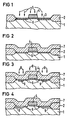
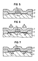
- FIGS. 1 to 7 represent the method steps essential to the invention in the sectional view.
- the process flow for producing n-channel MOS transistors is described.
- the method according to the invention can also be used for the production of p-channel MOS transistors and also for CMOS processes.
- the same reference numerals apply to the same parts in all figures.
- the intermediate oxide which can also consist of BPSG, is deposited in a layer thickness of - 500 nm and the arrangement is optionally subjected to a further flow process.
- the contact is made in a known manner.
Landscapes
- Insulated Gate Type Field-Effect Transistor (AREA)
- Metal-Oxide And Bipolar Metal-Oxide Semiconductor Integrated Circuits (AREA)
- Electrodes Of Semiconductors (AREA)
Claims (11)
Priority Applications (1)
| Application Number | Priority Date | Filing Date | Title |
|---|---|---|---|
| AT85104313T ATE32638T1 (de) | 1984-04-19 | 1985-04-10 | Verfahren zum herstellen von hochintegrierten mos-feldeffekttransistoren. |
Applications Claiming Priority (2)
| Application Number | Priority Date | Filing Date | Title |
|---|---|---|---|
| DE3415002 | 1984-04-19 | ||
| DE3415002 | 1984-04-19 |
Publications (2)
| Publication Number | Publication Date |
|---|---|
| EP0159617A1 EP0159617A1 (fr) | 1985-10-30 |
| EP0159617B1 true EP0159617B1 (fr) | 1988-02-24 |
Family
ID=6234107
Family Applications (1)
| Application Number | Title | Priority Date | Filing Date |
|---|---|---|---|
| EP85104313A Expired EP0159617B1 (fr) | 1984-04-19 | 1985-04-10 | Procédé pour fabriquer des transistors à effet de champ du type MOS à haute intégration |
Country Status (6)
| Country | Link |
|---|---|
| US (1) | US4603472A (fr) |
| EP (1) | EP0159617B1 (fr) |
| JP (1) | JPS60235474A (fr) |
| AT (1) | ATE32638T1 (fr) |
| CA (1) | CA1237537A (fr) |
| DE (1) | DE3561680D1 (fr) |
Families Citing this family (13)
| Publication number | Priority date | Publication date | Assignee | Title |
|---|---|---|---|---|
| US5140387A (en) * | 1985-11-08 | 1992-08-18 | Lockheed Missiles & Space Company, Inc. | Semiconductor device in which gate region is precisely aligned with source and drain regions |
| US4755479A (en) * | 1986-02-17 | 1988-07-05 | Fujitsu Limited | Manufacturing method of insulated gate field effect transistor using reflowable sidewall spacers |
| JPH01123417A (ja) * | 1987-11-07 | 1989-05-16 | Mitsubishi Electric Corp | 半導体装置の製造方法 |
| US5030582A (en) * | 1988-10-14 | 1991-07-09 | Matsushita Electric Industrial Co., Ltd. | Method of fabricating a CMOS semiconductor device |
| JPH0442579A (ja) * | 1990-06-08 | 1992-02-13 | Seiko Epson Corp | 薄膜トランジスタ及び製造方法 |
| US5166087A (en) * | 1991-01-16 | 1992-11-24 | Sharp Kabushiki Kaisha | Method of fabricating semiconductor element having lightly doped drain (ldd) without using sidewalls |
| TW201848B (fr) * | 1991-11-08 | 1993-03-11 | Advanced Micro Devices Inc | |
| US5512506A (en) * | 1995-04-06 | 1996-04-30 | Advanced Micro Devices, Inc. | Lightly doped drain profile optimization with high energy implants |
| JPH10125906A (ja) * | 1996-10-18 | 1998-05-15 | Rohm Co Ltd | 半導体装置及びその製造方法 |
| US6054356A (en) * | 1996-12-10 | 2000-04-25 | Advanced Micro Devices, Inc. | Transistor and process of making a transistor having an improved LDD masking material |
| US5994210A (en) * | 1997-08-12 | 1999-11-30 | National Semiconductor Corporation | Method of improving silicide sheet resistance by implanting fluorine |
| EP1017087A1 (fr) * | 1998-12-29 | 2000-07-05 | STMicroelectronics S.r.l. | Procédé de fabrication pour un transistor MOS intégré au substrat semi-conducteur |
| CN100418200C (zh) * | 2005-05-19 | 2008-09-10 | 上海宏力半导体制造有限公司 | 源极/漏极离子掺杂方法 |
Family Cites Families (12)
| Publication number | Priority date | Publication date | Assignee | Title |
|---|---|---|---|---|
| US440473A (en) * | 1890-11-11 | Friction-wrench | ||
| JPS54147789A (en) * | 1978-05-11 | 1979-11-19 | Matsushita Electric Ind Co Ltd | Semiconductor divice and its manufacture |
| JPS55138874A (en) * | 1979-04-18 | 1980-10-30 | Fujitsu Ltd | Semiconductor device and method of fabricating the same |
| JPS5693367A (en) * | 1979-12-20 | 1981-07-28 | Fujitsu Ltd | Manufacture of semiconductor device |
| US4356623A (en) * | 1980-09-15 | 1982-11-02 | Texas Instruments Incorporated | Fabrication of submicron semiconductor devices |
| US4345366A (en) * | 1980-10-20 | 1982-08-24 | Ncr Corporation | Self-aligned all-n+ polysilicon CMOS process |
| US4366613A (en) * | 1980-12-17 | 1983-01-04 | Ibm Corporation | Method of fabricating an MOS dynamic RAM with lightly doped drain |
| CA1197926A (fr) * | 1981-12-16 | 1985-12-10 | William D. Ryden | Drain sans chevauchement et contacts auto-alignes pour dispositif mos |
| DE3211761A1 (de) * | 1982-03-30 | 1983-10-06 | Siemens Ag | Verfahren zum herstellen von integrierten mos-feldeffekttransistorschaltungen in siliziumgate-technologie mit silizid beschichteten diffusionsgebieten als niederohmige leiterbahnen |
| US4499653A (en) * | 1983-11-03 | 1985-02-19 | Westinghouse Electric Corp. | Small dimension field effect transistor using phosphorous doped silicon glass reflow process |
| US4532697A (en) * | 1983-12-02 | 1985-08-06 | At&T Bell Laboratories | Silicon gigabit metal-oxide-semiconductor device processing |
| US4535528A (en) * | 1983-12-02 | 1985-08-20 | Hewlett-Packard Company | Method for improving reflow of phosphosilicate glass by arsenic implantation |
-
1985
- 1985-01-24 US US06/694,295 patent/US4603472A/en not_active Expired - Fee Related
- 1985-04-10 DE DE8585104313T patent/DE3561680D1/de not_active Expired
- 1985-04-10 AT AT85104313T patent/ATE32638T1/de not_active IP Right Cessation
- 1985-04-10 EP EP85104313A patent/EP0159617B1/fr not_active Expired
- 1985-04-17 JP JP60082102A patent/JPS60235474A/ja active Pending
- 1985-04-17 CA CA000479324A patent/CA1237537A/fr not_active Expired
Also Published As
| Publication number | Publication date |
|---|---|
| EP0159617A1 (fr) | 1985-10-30 |
| CA1237537A (fr) | 1988-05-31 |
| US4603472A (en) | 1986-08-05 |
| DE3561680D1 (en) | 1988-03-31 |
| ATE32638T1 (de) | 1988-03-15 |
| JPS60235474A (ja) | 1985-11-22 |
Similar Documents
| Publication | Publication Date | Title |
|---|---|---|
| DE3888883T2 (de) | Verfahren zur Herstellung einer vergrabenen isolierenden Schicht in einem Halbleitersubstrat durch Ionenimplantation und Halbleiterstruktur mit einer solchen Schicht. | |
| DE4406849C2 (de) | Verfahren zur Herstellung eines MOS-Transistors mit einem einen flachen Übergang aufweisenden Source/Drain-Bereich und einer Silicidschicht | |
| DE69121535T2 (de) | Feldeffekttransistor mit inverser T-förmiger Silizid-Torelektrode | |
| DE10214066B4 (de) | Halbleiterbauelement mit retrogradem Dotierprofil in einem Kanalgebiet und Verfahren zur Herstellung desselben | |
| DE3019850C2 (fr) | ||
| DE3685970T2 (de) | Verfahren zum herstellen eines halbleiterbauelements. | |
| DE3886074T2 (de) | Herstellung einer Halbleiterstruktur. | |
| DE69128554T2 (de) | Verfahren zur Herstellung einer integrierten Schaltungsstruktur mit niedrig dotiertem Drain und eine MOS-integrierte Schaltungsstruktur | |
| DE68911715T2 (de) | Dünnfilm-Transistor zum Betrieb für hohe Spannungen und dessen Herstellungsverfahren. | |
| EP0224199B1 (fr) | Procédé pour fabriquer des circuits très intégrés comportant des transistors du type MOS à canal P et à canal N avec des électrodes à grille comportant une couche dopée double en polysilicium et siliciure métallique | |
| DE69215547T2 (de) | Methode zur Herstellung eines Feldeffekttransistors | |
| EP0118709A2 (fr) | Procédé pour la fabrication de transistor MOS à régions de source et drain planaires, à courte longueur de canal et à niveau de contact auto-aligné comportant un siliciure métallique | |
| DE3326534A1 (de) | Schottkybarrieren-mos-bauelemente | |
| DE19527131A1 (de) | Halbleitervorrichtung und Verfahren zu deren Herstellung | |
| DE3211761A1 (de) | Verfahren zum herstellen von integrierten mos-feldeffekttransistorschaltungen in siliziumgate-technologie mit silizid beschichteten diffusionsgebieten als niederohmige leiterbahnen | |
| DE3150222A1 (de) | "verfahren zum herstellen einer halbleitervorrichtung" | |
| EP0268941A1 (fr) | Structure d'un transistor à effet de champ du type MOS comportant des régions de source et drain et des régions de connexion en silicide, ainsi que procédé de fabrication dans un tel circuit intégré | |
| DE2845460A1 (de) | Verfahren zur herstellung einer halbleitervorrichtung | |
| EP0482232A1 (fr) | Méthode de fabrication d'une couche de polycide dopée sur un substrat semi-conducteur | |
| DE3636249A1 (de) | Verfahren zum herstellen eines mos-feldeffekttransistors und danach hergestellter transistor | |
| DE3230077A1 (de) | Integrierte bipolar- und mos-transistoren enthaltende halbleiterschaltung auf einem chip und verfahren zu ihrer herstellung | |
| EP0072967B1 (fr) | Procédé pour la fabrication de circuits à transistors à effet de champ complémentaire à haute densité d'intégration en technologie d'électrode de porte en silicium | |
| EP0159617A1 (fr) | Procédé pour fabriquer des transistors à effet de champ du type MOS à haute intégration | |
| DE69131376T2 (de) | Verfahren zur Herstellung von doppelt-diffundierten integrierten MOSFET-Zellen | |
| DE3324332A1 (de) | Verfahren zur herstellung von cmos-transistoren auf einem siliziumsubstrat |
Legal Events
| Date | Code | Title | Description |
|---|---|---|---|
| PUAI | Public reference made under article 153(3) epc to a published international application that has entered the european phase |
Free format text: ORIGINAL CODE: 0009012 |
|
| AK | Designated contracting states |
Designated state(s): AT CH DE FR GB IT LI NL SE |
|
| 17P | Request for examination filed |
Effective date: 19850827 |
|
| 17Q | First examination report despatched |
Effective date: 19870514 |
|
| GRAA | (expected) grant |
Free format text: ORIGINAL CODE: 0009210 |
|
| AK | Designated contracting states |
Kind code of ref document: B1 Designated state(s): AT CH DE FR GB IT LI NL SE |
|
| REF | Corresponds to: |
Ref document number: 32638 Country of ref document: AT Date of ref document: 19880315 Kind code of ref document: T |
|
| REF | Corresponds to: |
Ref document number: 3561680 Country of ref document: DE Date of ref document: 19880331 |
|
| ET | Fr: translation filed | ||
| ITF | It: translation for a ep patent filed | ||
| GBT | Gb: translation of ep patent filed (gb section 77(6)(a)/1977) | ||
| PLBE | No opposition filed within time limit |
Free format text: ORIGINAL CODE: 0009261 |
|
| STAA | Information on the status of an ep patent application or granted ep patent |
Free format text: STATUS: NO OPPOSITION FILED WITHIN TIME LIMIT |
|
| 26N | No opposition filed | ||
| PG25 | Lapsed in a contracting state [announced via postgrant information from national office to epo] |
Ref country code: GB Effective date: 19890410 Ref country code: AT Effective date: 19890410 |
|
| PG25 | Lapsed in a contracting state [announced via postgrant information from national office to epo] |
Ref country code: SE Effective date: 19890411 |
|
| PG25 | Lapsed in a contracting state [announced via postgrant information from national office to epo] |
Ref country code: LI Effective date: 19890430 Ref country code: CH Effective date: 19890430 |
|
| PG25 | Lapsed in a contracting state [announced via postgrant information from national office to epo] |
Ref country code: NL Effective date: 19891101 |
|
| GBPC | Gb: european patent ceased through non-payment of renewal fee | ||
| NLV4 | Nl: lapsed or anulled due to non-payment of the annual fee | ||
| PG25 | Lapsed in a contracting state [announced via postgrant information from national office to epo] |
Ref country code: FR Free format text: LAPSE BECAUSE OF NON-PAYMENT OF DUE FEES Effective date: 19891228 |
|
| REG | Reference to a national code |
Ref country code: CH Ref legal event code: PL |
|
| PG25 | Lapsed in a contracting state [announced via postgrant information from national office to epo] |
Ref country code: DE Effective date: 19900103 |
|
| REG | Reference to a national code |
Ref country code: FR Ref legal event code: ST |
|
| EUG | Se: european patent has lapsed |
Ref document number: 85104313.3 Effective date: 19900412 |