EP0482232A1 - Méthode de fabrication d'une couche de polycide dopée sur un substrat semi-conducteur - Google Patents
Méthode de fabrication d'une couche de polycide dopée sur un substrat semi-conducteur Download PDFInfo
- Publication number
- EP0482232A1 EP0482232A1 EP90120324A EP90120324A EP0482232A1 EP 0482232 A1 EP0482232 A1 EP 0482232A1 EP 90120324 A EP90120324 A EP 90120324A EP 90120324 A EP90120324 A EP 90120324A EP 0482232 A1 EP0482232 A1 EP 0482232A1
- Authority
- EP
- European Patent Office
- Prior art keywords
- layer
- implantation
- gate electrode
- mos transistor
- silicon
- Prior art date
- Legal status (The legal status is an assumption and is not a legal conclusion. Google has not performed a legal analysis and makes no representation as to the accuracy of the status listed.)
- Granted
Links
Images

Classifications
-
- H—ELECTRICITY
- H10—SEMICONDUCTOR DEVICES; ELECTRIC SOLID-STATE DEVICES NOT OTHERWISE PROVIDED FOR
- H10P—GENERIC PROCESSES OR APPARATUS FOR THE MANUFACTURE OR TREATMENT OF DEVICES COVERED BY CLASS H10
- H10P14/00—Formation of materials, e.g. in the shape of layers or pillars
- H10P14/40—Formation of materials, e.g. in the shape of layers or pillars of conductive or resistive materials
-
- H—ELECTRICITY
- H10—SEMICONDUCTOR DEVICES; ELECTRIC SOLID-STATE DEVICES NOT OTHERWISE PROVIDED FOR
- H10P—GENERIC PROCESSES OR APPARATUS FOR THE MANUFACTURE OR TREATMENT OF DEVICES COVERED BY CLASS H10
- H10P32/00—Diffusion of dopants within, into or out of wafers, substrates or parts of devices
- H10P32/30—Diffusion for doping of conductive or resistive layers
-
- H—ELECTRICITY
- H10—SEMICONDUCTOR DEVICES; ELECTRIC SOLID-STATE DEVICES NOT OTHERWISE PROVIDED FOR
- H10D—INORGANIC ELECTRIC SEMICONDUCTOR DEVICES
- H10D64/00—Electrodes of devices having potential barriers
- H10D64/01—Manufacture or treatment
- H10D64/013—Manufacture or treatment of electrodes having a conductor capacitively coupled to a semiconductor by an insulator
- H10D64/01302—Manufacture or treatment of electrodes having a conductor capacitively coupled to a semiconductor by an insulator the insulator being formed after the semiconductor body, the semiconductor being silicon
- H10D64/01304—Manufacture or treatment of electrodes having a conductor capacitively coupled to a semiconductor by an insulator the insulator being formed after the semiconductor body, the semiconductor being silicon characterised by the conductor
- H10D64/01306—Manufacture or treatment of electrodes having a conductor capacitively coupled to a semiconductor by an insulator the insulator being formed after the semiconductor body, the semiconductor being silicon characterised by the conductor the conductor comprising a layer of silicon contacting the insulator, e.g. polysilicon
- H10D64/01308—Manufacture or treatment of electrodes having a conductor capacitively coupled to a semiconductor by an insulator the insulator being formed after the semiconductor body, the semiconductor being silicon characterised by the conductor the conductor comprising a layer of silicon contacting the insulator, e.g. polysilicon the conductor further comprising a non-elemental silicon additional conductive layer, e.g. a metal silicide layer formed by the reaction of silicon with an implanted metal
- H10D64/0131—Manufacture or treatment of electrodes having a conductor capacitively coupled to a semiconductor by an insulator the insulator being formed after the semiconductor body, the semiconductor being silicon characterised by the conductor the conductor comprising a layer of silicon contacting the insulator, e.g. polysilicon the conductor further comprising a non-elemental silicon additional conductive layer, e.g. a metal silicide layer formed by the reaction of silicon with an implanted metal the additional conductive layer comprising a silicide layer formed by the silicidation reaction between the layer of silicon with a metal layer which is not formed by metal implantation
-
- H—ELECTRICITY
- H10—SEMICONDUCTOR DEVICES; ELECTRIC SOLID-STATE DEVICES NOT OTHERWISE PROVIDED FOR
- H10D—INORGANIC ELECTRIC SEMICONDUCTOR DEVICES
- H10D84/00—Integrated devices formed in or on semiconductor substrates that comprise only semiconducting layers, e.g. on Si wafers or on GaAs-on-Si wafers
- H10D84/01—Manufacture or treatment
- H10D84/0123—Integrating together multiple components covered by H10D12/00 or H10D30/00, e.g. integrating multiple IGBTs
- H10D84/0126—Integrating together multiple components covered by H10D12/00 or H10D30/00, e.g. integrating multiple IGBTs the components including insulated gates, e.g. IGFETs
- H10D84/0165—Integrating together multiple components covered by H10D12/00 or H10D30/00, e.g. integrating multiple IGBTs the components including insulated gates, e.g. IGFETs the components including complementary IGFETs, e.g. CMOS devices
- H10D84/0172—Manufacturing their gate conductors
- H10D84/0174—Manufacturing their gate conductors the gate conductors being silicided
-
- H—ELECTRICITY
- H10—SEMICONDUCTOR DEVICES; ELECTRIC SOLID-STATE DEVICES NOT OTHERWISE PROVIDED FOR
- H10D—INORGANIC ELECTRIC SEMICONDUCTOR DEVICES
- H10D84/00—Integrated devices formed in or on semiconductor substrates that comprise only semiconducting layers, e.g. on Si wafers or on GaAs-on-Si wafers
- H10D84/01—Manufacture or treatment
- H10D84/02—Manufacture or treatment characterised by using material-based technologies
- H10D84/03—Manufacture or treatment characterised by using material-based technologies using Group IV technology, e.g. silicon technology or silicon-carbide [SiC] technology
- H10D84/038—Manufacture or treatment characterised by using material-based technologies using Group IV technology, e.g. silicon technology or silicon-carbide [SiC] technology using silicon technology, e.g. SiGe
-
- H—ELECTRICITY
- H10—SEMICONDUCTOR DEVICES; ELECTRIC SOLID-STATE DEVICES NOT OTHERWISE PROVIDED FOR
- H10D—INORGANIC ELECTRIC SEMICONDUCTOR DEVICES
- H10D84/00—Integrated devices formed in or on semiconductor substrates that comprise only semiconducting layers, e.g. on Si wafers or on GaAs-on-Si wafers
- H10D84/80—Integrated devices formed in or on semiconductor substrates that comprise only semiconducting layers, e.g. on Si wafers or on GaAs-on-Si wafers characterised by the integration of at least one component covered by groups H10D12/00 or H10D30/00, e.g. integration of IGFETs
- H10D84/82—Integrated devices formed in or on semiconductor substrates that comprise only semiconducting layers, e.g. on Si wafers or on GaAs-on-Si wafers characterised by the integration of at least one component covered by groups H10D12/00 or H10D30/00, e.g. integration of IGFETs of only field-effect components
- H10D84/83—Integrated devices formed in or on semiconductor substrates that comprise only semiconducting layers, e.g. on Si wafers or on GaAs-on-Si wafers characterised by the integration of at least one component covered by groups H10D12/00 or H10D30/00, e.g. integration of IGFETs of only field-effect components of only insulated-gate FETs [IGFET]
- H10D84/85—Complementary IGFETs, e.g. CMOS
- H10D84/859—Complementary IGFETs, e.g. CMOS comprising both N-type and P-type wells, e.g. twin-tub
Definitions
- doped polycide layers that is to say composite layers composed of a doped silicon layer which is polycrystalline or amorphous and a metal silicide layer arranged thereon, are becoming increasingly important.
- Doped polycide layers are used, for example, in bipolar technology as a connection structure for the emitter, base and collector and in CMOS technology as gate electrodes.
- doped polycide layers are produced, inter alia, by applying a metal layer to a doped silicon layer which is arranged on a semiconductor substrate and is polycrystalline or amorphous. With the help of a temperature treatment, part of the silicon layer reacts with the metal layer arranged thereon to form metal silicide. This leads to a dopant depletion of the remaining part of the silicon layer. There is a backflow of dopant from the silicon into the metal silicide. This effect is particularly strong when boron is used as a dopant. The dopant depletion is explained by a parasitic metal-dopant reaction that takes place during silicide formation and that leads to the formation of stable metal-dopant compounds, such as TiB 2 .
- the salicide process is the simultaneous siliconization of the gate electrode and source / drain regions in the production of MOS transistors.
- a metal for example titanium
- the formation of silicide occurs on the exposed silicon surfaces, that is to say the surface of a gate electrode made of polysilicon or amorphous silicon and the substrate surface in the source / drain regions, whereas the unreacted metal is retained in regions masked with silicon oxide or silicon nitride.
- the metal and possibly reaction products are selectively removed to the metal silicide, so that the metal silicide remains only on the gate electrode and the source / drain regions.
- a reduction of the layer and contact resistances to improve the transistor performance is achieved.
- the salicide process is described, for example, in M.E. Alperin et al., IEEE Trans. Electron Devices, ED-32, 141 (1985).
- the invention is therefore based on the object of specifying a method for producing a doped polycide layer in which dopant depletion is avoided and which is compatible with the salicide process.
- the major part of the dopant depletion takes place in the known processes during the siliconization reaction. Therefore, the dopant depletion is avoided in the method according to the invention in that the final dopant distribution in the polycide layer by Implantation after the silicidation reaction is established. This has the advantage that the siliconization reaction can be carried out without restrictions.
- the silicon layer with a preliminary doping before the metal silicide layer is produced.
- This embodiment is particularly advantageous when using boron doping, since the maximum achievable doping in silicon is limited anyway due to the relatively low solubility of boron in silicon.
- the known methods of co-sputtering of metal and silicon, CVD deposition of the metal silicide and deposition of the metal on the silicon layer with subsequent heat treatment are suitable for producing the metal silicide layer. It is particularly advantageous to produce the metal silicide layer by depositing a metal layer on the silicon layer with subsequent heat treatment. This reaction takes place selectively between metal and silicon, so that areas on the surface of the silicon layer which are not to be siliconized, e.g. B. Si0 2 or Si3N4 can be masked.
- Source and drain regions for the MOS transistor are produced during the implantation after the siliconization reaction.
- both the gate electrode and the surface of the source / drain regions are siliconized in the salicide process. Since, according to the invention, the implantation of the source / drain regions takes place only after the siliconization reaction, doping of the source / drain regions is also avoided.
- n-channel transistor is designed as a buried channel device and the p-channel transistor as a surface-channel MOSFET. This leads to a significant increase in transistor life and can therefore be used advantageously for a 5-volt application.
- a further embodiment of the invention consists in its application in an overall salicide CMOS process for the production of n-channel transistors with n -doped polycide gates and with p-channel transistors with p -doped polyzide gates (so-called dual work function gates).
- both the n-channel transistors and the p-channel transistors are manufactured as surface-channel MOSFETs. These have excellent short-channel behavior.
- This embodiment can therefore be used advantageously for the production of CMOS circuits with transistors with a short gate length, which can be operated with a reduced supply voltage.
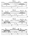
- a polysilicon layer 12 is applied to a substrate 11 (see FIG. 1) made of, for example, monocrystalline silicon.
- the polysilicon layer 12 is undoped.
- a metal layer 13 is applied to the polysilicon layer 12, which consists, for example, of titanium, tantalum, tungsten, molybdenum, cobalt, nickel or platinum.
- the polysilicon layer 12 has a thickness of, for example, 100 to 500 nm.
- the metal layer 13 is z. B. 60 nm deposited.
- a metal silicide layer 13a is formed by reaction between the metal of the metal layer 13 and part of the polysilicon layer 12 (see FIG. 2). The remaining part of the polysilicon layer 12a forms a polycide layer 14 with the metal silicide layer 13a.
- metal silicide layer 13a by simultaneous sputtering of the metal and the silicon with subsequent temperature treatment for the formation of silicide or by CVD deposition.
- the polycide layer 14 is doped by implantation, indicated by the reference symbol 15 in FIG If TiSi 2 with the dopant boron is the case, the implantation 15 must be carried out with such energy that dopant ions at least up to the interface of the polysilicon layer 12a with the metal silicide layer 13a arrive. In this case, a diffusion of dopant out of the metal silicide layer 13a is impossible because of the strong, competing metal-dopant reaction.
- the polysilicon layer 12 with a pre-doping before the metal layer 13 is deposited or the polysilicon layer 12a before the metal silicide layer 13a is produced.
- the siliconization reaction leads to a dopant depletion of the polysilicon layer 12a, this is compensated for by the subsequent implantation 15.
- the final dopant profile is determined by the implantation 15 after the polycide layer 14 has been formed.
- the first trough 22 is doped with boron, for example, and has a dopant concentration of, for example, 5 ⁇ 10 16 cm ⁇ 3 .
- the second well 23 is, for example doped with phosphorus and has a Dotierstoffkon- zen t ra ti on on of 5 x 10 16 cm-. 3
- a first region for receiving a first MOS transistor is defined in the first well 22 and a second region for receiving a second MOS transistor complementary to the first is defined in the second well 23.
- the field oxide areas serve to separate the active transistors.
- the field oxide regions 24, the first well 22 and the second well 23 are produced, for example, using LOCOS technology.
- the first MOS transistor is manufactured as an NMOS transistor and the second MOS transistor as a PMOS transistor.
- a gate oxide layer 25 is produced on the surface of the first tub 22 and the second tub 23 in a known manner.
- a polysilicon layer 26 is deposited over the entire surface.
- the polysilicon layer 26 is produced in a thickness of, for example, 100 to 500 nm and p-doped by implantation of, for example, boron.
- the implantation is carried out with an energy of 15 keV and a dose of 5 x 10 11 cm - 2.
- a cover layer 27 made of, for example, silicon nitride or silicon oxide is deposited on the polysilicon layer 26.
- the cover layer 27 is produced in a thickness of, for example, 150 nm.
- the cover layer 27 and the polysilicon layer 26 are structured with the aid of a photo technology (not shown) in such a way that a first gate electrode 26a for the first MOS transistor and a second gate electrode 26b for the second MOS transistor are formed from the polysilicon layer 26.
- flanks of the first gate electrode 26a and the second gate electrode 26b are covered with thin flank oxides 28. This is followed by the production of a first photoresist mask 29, which only leaves the first area uncovered (see FIG. 5).
- LDD source / drain regions 30 are generated for the first MOS transistor.
- the first photoresist mask 29 and the first gate electrode 26a serve as an implantation mask.
- the implantation of phosphorus ions in the first gate electrode 26a is prevented by the cover layer 27a and the side oxides 28.
- flank coverings 31 made of, for example, silicon oxide are produced on the flanks of the first gate electrode 26a and the second gate electrode 26b.
- highly doped source / drain regions 33 are produced for the first MOS transistor by implantation with arsenic. Since the flank coverings 31 are wider than the flank oxides 28, the extent of the highly doped source / drain regions 33 is less than that of the LDD source / drain regions 30 (see FIG. 6).
- the structured cover layer 27a is removed.
- the source / drain regions 30, 33 can be activated, which has an advantageous effect on the subsequent siliconization.
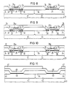
- first gate electrode 26a and the second gate electrode 26b and on the surface of the first well 22 and the second well 23 is applied by applying a metal layer 340 made of z. B. titanium (see FIG. 7) and subsequent temperature treatment at, for example, 600 to 1000 ° C. metal silicide 34 (see FIG. 8). This leads to a dopant depletion in the first gate electrode 26a and in the second gate electrode 26b.
- the dopant depletion in the second gate electrode 26b is compensated for by implantation with, for example, boron.
- source / drain regions 36 for the second MOS transistor are implanted (see FIG. 9).
- the boron implantation is carried out, for example, with an energy of 30 keV and a dose of 5 x 10 15 cm-. 2
- the boron implantation must be deep enough to reach the interface between metal silicide and polysilicon in the second gate electrode 26b.
- the boron implantation must not be too deep so that the source / drain regions 36 meet the requirements for a short-channel transistor.
- the second photoresist mask 35 shields the first gate electrode 26a from the implantation with boron.
- the dopant depletion is not critical since, in contrast to the second MOS transistor, which is a PMOS-FET, no space charge zone is formed in the gate electrode 26a in the first MOS transistor, which is an NMOS-FET.
- an intermediate oxide layer 37 (see FIG. 10) is applied over the entire surface.
- Flow tempering follows to activate the post-implanted dopant. The flow tempering takes place, for example, at 900 ° C.
- a first well 42, for example p-doped, and a second well 43, for example n-doped, are produced in a substrate 41 made of, for example, monocrystalline silicon.
- the first well is doped with boron in a concentration of 5 x 10 16 cm -3 .
- the second well 43 is doped, for example, with phosphorus in a dopant concentration of 5 x 10 16 cm -3 .
- the field oxide regions 44 are provided to separate active transistor regions.
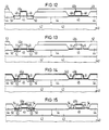
- the field oxide regions 44 and the first well 42 and the second well 43 are produced, for example, using LOCOS technology (see FIG. 11).
- the first well 42 has a first region which is uncovered by the field oxide regions 44 and which is intended for receiving a first MOS transistor.
- the second well 43 has a second region which is not covered by the field oxide regions 44 and which is intended for receiving a second MOS transistor.
- Channel implants (not shown) for the first MOS transistor, which is an NMOS FET, are provided on the surface of the first region.
- Channel implants are provided on the surface of the second region for the second MOS transistor, which is a PMOS-FET.
- the exposed surface of the first well 42 and the second well 43 is provided with a gate oxide layer 45 in a known manner.
- An undoped polysilicon layer 46 is deposited over the entire surface in a thickness of, for example, 100 to 500 nm.
- a first photoresist mask 47 After forming a first photoresist mask 47, is only the second can region uncovered carried out an implantation with boron at an energy of, for example, 15 keV and a dose of, for example, 5 x 10 15 cm- 2 for p-doping of the polysilicon layer 46th
- a first gate electrode 46a and a second gate electrode 46b are produced by structuring the polysilicon layer 46.
- the first gate electrode 46a is arranged in the region of the first MOS transistor and, according to the manufacture, consists of undoped polysilicon (see FIG. 12).
- the second gate electrode 46b lies in the region of the second MOS transistor and, according to the manufacture, consists of p-doped polysilicon.
- thin flank oxides 48 are generated on the flanks of the first gate electrode 46a and the second gate electrode 46b.
- an implantation with phosphorus is carried out to form LDD source / drain regions 50 for the first MOS transistor (see FIG. 12).
- the implantation is carried out, for example, with the following parameters: energy 60 keV, dose: 3 x 10 13 cm-. 2
- flank coverings 51 made of, for example, silicon oxide or silicon nitride are produced on the flanks of the first gate electrode 46a and the second gate electrode 46b.
- highly doped source / drain regions 53 for the first MOS transistor are produced by an arsenic implantation.
- the first gate electrode 46a is n ⁇ doped (see FIG. 13). Since the extent of the flank coverings 51 is greater than that of the flank oxides 48, the highly doped source / drain regions 53 have a different extent than the LDD source / drain regions 50.
- the arsenic implantation is carried out, for example, with the following parameters: energy 50 keV, dose: 5 x 10 15 cm-. 2
- a metal layer 540 made of, for example, titanium is applied over the entire surface (see FIG. 14).
- metal silicide 54 for example TiSi 2
- metal silicide 54 is selectively formed on the exposed silicon surfaces of the first well 42 and the second well 43 and on the surface of the first gate electrode 46a and the second gate electrode 46b made of polysilicon. generated (see Figure 15).
- a dopant depletion occurs in the second gate electrode 46b as a result of the metal dopant reaction between titanium and boron.
- Such a metal dopant reaction takes place in the first gate electrode 46a between arsenic and titanium does not take place to any appreciable extent, so that one cannot speak of a dopant depletion here.
- a boron implantation is carried out to compensate for the dopant depletion in the second gate electrode 46b.
- the boron implantation is carried out, for example, with the following parameters: energy 30 keV, dose: 5 x 10 15 cm- 2
- the dopant When implanting with boron, care must be taken that the dopant reaches at least the interface between the metal silicide 54 and the polysilicon in the second electrode 46b. Because of the strong metal dopant reaction, later diffusion of boron out of the metal silicide 54 into the polysilicon is not possible. On the other hand, the boron implantation must be carried out so that the source / drain regions 56 meet the requirements for the second MOS transistor (see FIG. 16).
- an intermediate oxide layer 57 is produced over the entire surface (see FIG. 17) and the structure is subjected to flow tempering at, for example, 900 ° C.
- the source / drain regions 56 of the second MOS transistor are activated during the flow tempering. If not already done, the highly doped source / drain regions 53 and the LDD source / drain regions 50 of the first MOS transistor are likewise activated in this step.
- the manufacturing process is ended in a known manner with contact hole etching and metallization.
Landscapes
- Electrodes Of Semiconductors (AREA)
- Metal-Oxide And Bipolar Metal-Oxide Semiconductor Integrated Circuits (AREA)
- Insulated Gate Type Field-Effect Transistor (AREA)
- Internal Circuitry In Semiconductor Integrated Circuit Devices (AREA)
- Recrystallisation Techniques (AREA)
Priority Applications (6)
| Application Number | Priority Date | Filing Date | Title |
|---|---|---|---|
| AT90120324T ATE139058T1 (de) | 1990-10-23 | 1990-10-23 | Verfahren zur herstellung einer dotierten polyzidschicht auf einem halbleitersubstrat |
| DE59010362T DE59010362D1 (de) | 1990-10-23 | 1990-10-23 | Verfahren zur Herstellung einer dotierten Polyzidschicht auf einem Halbleitersubstrat |
| EP90120324A EP0482232B1 (fr) | 1990-10-23 | 1990-10-23 | Méthode de fabrication d'une couche de polycide dopée sur un substrat semi-conducteur |
| US07/779,408 US5190888A (en) | 1990-10-23 | 1991-10-17 | Method for producing a doped polycide layer on a semiconductor substrate |
| JP29814691A JP3153587B2 (ja) | 1990-10-23 | 1991-10-18 | 半導体基板上にドープされたポリサイド層を製造する方法 |
| KR1019910018777A KR100241170B1 (ko) | 1990-10-23 | 1991-10-23 | 반도체 기판 상에 도핑된 폴리시드층을 생성시키는 방법 |
Applications Claiming Priority (1)
| Application Number | Priority Date | Filing Date | Title |
|---|---|---|---|
| EP90120324A EP0482232B1 (fr) | 1990-10-23 | 1990-10-23 | Méthode de fabrication d'une couche de polycide dopée sur un substrat semi-conducteur |
Publications (2)
| Publication Number | Publication Date |
|---|---|
| EP0482232A1 true EP0482232A1 (fr) | 1992-04-29 |
| EP0482232B1 EP0482232B1 (fr) | 1996-06-05 |
Family
ID=8204644
Family Applications (1)
| Application Number | Title | Priority Date | Filing Date |
|---|---|---|---|
| EP90120324A Expired - Lifetime EP0482232B1 (fr) | 1990-10-23 | 1990-10-23 | Méthode de fabrication d'une couche de polycide dopée sur un substrat semi-conducteur |
Country Status (6)
| Country | Link |
|---|---|
| US (1) | US5190888A (fr) |
| EP (1) | EP0482232B1 (fr) |
| JP (1) | JP3153587B2 (fr) |
| KR (1) | KR100241170B1 (fr) |
| AT (1) | ATE139058T1 (fr) |
| DE (1) | DE59010362D1 (fr) |
Families Citing this family (25)
| Publication number | Priority date | Publication date | Assignee | Title |
|---|---|---|---|---|
| JP3395263B2 (ja) * | 1992-07-31 | 2003-04-07 | セイコーエプソン株式会社 | 半導体装置およびその製造方法 |
| JPH07312353A (ja) * | 1994-05-17 | 1995-11-28 | Fuji Electric Co Ltd | 半導体装置の製造方法 |
| US5416038A (en) * | 1994-05-25 | 1995-05-16 | United Microelectronics Corporation | Method for producing semiconductor device with two different threshold voltages |
| US5824577A (en) * | 1995-02-16 | 1998-10-20 | National Semiconductor Corporation | MOSFET with reduced leakage current |
| JPH08264660A (ja) * | 1995-03-24 | 1996-10-11 | Nec Corp | 半導体装置の製造方法 |
| US5759886A (en) * | 1995-09-28 | 1998-06-02 | National Semiconductor Corporation | Method for forming a layer of metal silicide over the gates of a surface-channel CMOS device |
| KR100365937B1 (ko) * | 1995-12-29 | 2003-03-03 | 주식회사 하이닉스반도체 | 구리금속배선형성방법 |
| US6028339A (en) * | 1996-08-29 | 2000-02-22 | International Business Machines Corporation | Dual work function CMOS device |
| US5770490A (en) * | 1996-08-29 | 1998-06-23 | International Business Machines Corporation | Method for producing dual work function CMOS device |
| KR100268920B1 (ko) * | 1997-04-21 | 2000-12-01 | 김영환 | 반도체소자의제조방법 |
| US5956584A (en) * | 1998-03-30 | 1999-09-21 | Texas Instruments - Acer Incorporated | Method of making self-aligned silicide CMOS transistors |
| JPH11330385A (ja) * | 1998-05-20 | 1999-11-30 | Mitsumi Electric Co Ltd | Cmosデバイス |
| KR100308133B1 (ko) * | 1999-01-12 | 2001-09-26 | 김영환 | 듀얼 게이트 모스 트랜지스터 제조방법 |
| JP3235583B2 (ja) * | 1999-01-19 | 2001-12-04 | 日本電気株式会社 | 半導体装置の製造方法 |
| US6614082B1 (en) * | 1999-01-29 | 2003-09-02 | Micron Technology, Inc. | Fabrication of semiconductor devices with transition metal boride films as diffusion barriers |
| JP2001148428A (ja) * | 1999-11-18 | 2001-05-29 | Toshiba Microelectronics Corp | 半導体装置 |
| US7145191B1 (en) * | 2000-03-31 | 2006-12-05 | National Semiconductor Corporation | P-channel field-effect transistor with reduced junction capacitance |
| JP2002184716A (ja) * | 2000-12-11 | 2002-06-28 | Sharp Corp | 半導体装置の製造方法 |
| US6812529B2 (en) * | 2001-03-15 | 2004-11-02 | Micron Technology, Inc. | Suppression of cross diffusion and gate depletion |
| US6544888B2 (en) * | 2001-06-28 | 2003-04-08 | Promos Technologies, Inc. | Advanced contact integration scheme for deep-sub-150 nm devices |
| JP3781666B2 (ja) * | 2001-11-29 | 2006-05-31 | エルピーダメモリ株式会社 | ゲート電極の形成方法及びゲート電極構造 |
| US6770932B2 (en) * | 2002-07-10 | 2004-08-03 | Kabushiki Kaisha Toshiba | Semiconductor memory device having a memory region and a peripheral region, and a manufacturing method thereof |
| US7179700B2 (en) * | 2004-07-21 | 2007-02-20 | Freescale Semiconductor, Inc. | Semiconductor device with low resistance contacts |
| JP2007158220A (ja) * | 2005-12-08 | 2007-06-21 | Matsushita Electric Ind Co Ltd | 半導体装置の製造方法 |
| US10504899B2 (en) * | 2017-11-30 | 2019-12-10 | Taiwan Semiconductor Manufacturing Co., Ltd. | Transistors with various threshold voltages and method for manufacturing the same |
Citations (2)
| Publication number | Priority date | Publication date | Assignee | Title |
|---|---|---|---|---|
| FR2558010A1 (fr) * | 1984-01-10 | 1985-07-12 | Ates Componenti Elettron | Procede pour la fabrication de transistors mos complementaires a basses tensions de seuil dans des circuits integres a haute densite et structure resultant de ce procede |
| EP0163871A1 (fr) * | 1984-05-22 | 1985-12-11 | Siemens Aktiengesellschaft | Procédé pour fabriquer des électrodes de grille comportant des couches doubles de siliciure métallique à fusion élevée et de silicium polycristallin dopé |
Family Cites Families (9)
| Publication number | Priority date | Publication date | Assignee | Title |
|---|---|---|---|---|
| US4555842A (en) * | 1984-03-19 | 1985-12-03 | At&T Bell Laboratories | Method of fabricating VLSI CMOS devices having complementary threshold voltages |
| US4740479A (en) * | 1985-07-05 | 1988-04-26 | Siemens Aktiengesellschaft | Method for the manufacture of cross-couplings between n-channel and p-channel CMOS field effect transistors of static write-read memories |
| US4808548A (en) * | 1985-09-18 | 1989-02-28 | Advanced Micro Devices, Inc. | Method of making bipolar and MOS devices on same integrated circuit substrate |
| US4782033A (en) * | 1985-11-27 | 1988-11-01 | Siemens Aktiengesellschaft | Process for producing CMOS having doped polysilicon gate by outdiffusion of boron from implanted silicide gate |
| US4816423A (en) * | 1987-05-01 | 1989-03-28 | Texas Instruments Incorporated | Bicmos process for forming shallow npn emitters and mosfet source/drains |
| US5059546A (en) * | 1987-05-01 | 1991-10-22 | Texas Instruments Incorporated | BICMOS process for forming shallow NPN emitters and mosfet source/drains |
| US4933994A (en) * | 1987-06-11 | 1990-06-19 | General Electric Company | Method for fabricating a self-aligned lightly doped drain semiconductor device with silicide |
| JPH01238144A (ja) * | 1988-03-18 | 1989-09-22 | Sony Corp | 半導体装置の製造方法 |
| US4912061A (en) * | 1988-04-04 | 1990-03-27 | Digital Equipment Corporation | Method of forming a salicided self-aligned metal oxide semiconductor device using a disposable silicon nitride spacer |
-
1990
- 1990-10-23 AT AT90120324T patent/ATE139058T1/de not_active IP Right Cessation
- 1990-10-23 DE DE59010362T patent/DE59010362D1/de not_active Expired - Lifetime
- 1990-10-23 EP EP90120324A patent/EP0482232B1/fr not_active Expired - Lifetime
-
1991
- 1991-10-17 US US07/779,408 patent/US5190888A/en not_active Expired - Lifetime
- 1991-10-18 JP JP29814691A patent/JP3153587B2/ja not_active Expired - Lifetime
- 1991-10-23 KR KR1019910018777A patent/KR100241170B1/ko not_active Expired - Lifetime
Patent Citations (2)
| Publication number | Priority date | Publication date | Assignee | Title |
|---|---|---|---|---|
| FR2558010A1 (fr) * | 1984-01-10 | 1985-07-12 | Ates Componenti Elettron | Procede pour la fabrication de transistors mos complementaires a basses tensions de seuil dans des circuits integres a haute densite et structure resultant de ce procede |
| EP0163871A1 (fr) * | 1984-05-22 | 1985-12-11 | Siemens Aktiengesellschaft | Procédé pour fabriquer des électrodes de grille comportant des couches doubles de siliciure métallique à fusion élevée et de silicium polycristallin dopé |
Non-Patent Citations (1)
| Title |
|---|
| JOURNAL OF VACUUM SCIENCE & TECHNOLOGY B, Band 7, Nr. 1, Januar - Februar 1989, Seiten 120-126, New York, US; U. SCHWALKE et al: "Boron diffusion within TaSi2/poly-Si gates" * |
Also Published As
| Publication number | Publication date |
|---|---|
| EP0482232B1 (fr) | 1996-06-05 |
| US5190888A (en) | 1993-03-02 |
| JPH04263422A (ja) | 1992-09-18 |
| JP3153587B2 (ja) | 2001-04-09 |
| DE59010362D1 (de) | 1996-07-11 |
| KR920008842A (ko) | 1992-05-28 |
| ATE139058T1 (de) | 1996-06-15 |
| KR100241170B1 (ko) | 2000-03-02 |
Similar Documents
| Publication | Publication Date | Title |
|---|---|---|
| EP0482232B1 (fr) | Méthode de fabrication d'une couche de polycide dopée sur un substrat semi-conducteur | |
| EP0118709B1 (fr) | Procédé pour la fabrication de transistor MOS à régions de source et drain planaires, à courte longueur de canal et à niveau de contact auto-aligné comportant un siliciure métallique | |
| DE4406849C2 (de) | Verfahren zur Herstellung eines MOS-Transistors mit einem einen flachen Übergang aufweisenden Source/Drain-Bereich und einer Silicidschicht | |
| EP0244607B1 (fr) | Méthode pour fabriquer des transistors CMOS optimisés à effet de champ en technologie VLSI | |
| DE69032917T2 (de) | Verfahren zur Herstellung einer Hochspannungs-MIS-integrierten Schaltung | |
| DE69132695T2 (de) | CMOS-Verfahren mit Verwendung von zeitweilig angebrachten Siliciumnitrid-Spacern zum Herstellen von Transistoren (LDD) mit leicht dotiertem Drain | |
| DE69506951T2 (de) | Methode zur Bildung von Metallsilizidschichten auf Source- und Draingebiete | |
| DE69835203T2 (de) | Herstellungsverfahren für nmos und pmos bauelemente mit reduzierte maskierungsschritten | |
| DE69025806T2 (de) | Doppel-diffundiertes Drain-CMOS-Verfahren mit einer Gegendotierungstechnik | |
| DE3886074T2 (de) | Herstellung einer Halbleiterstruktur. | |
| DE69111929T2 (de) | Halbleiteranordnung auf einem dielektrischen isolierten Substrat. | |
| EP0123182B1 (fr) | Procédé pour la fabrication de circuits intégrés à haute densité comportant des transistors à effet de champ du type MOS complémentaires | |
| EP0163871B1 (fr) | Procédé pour fabriquer des électrodes de grille comportant des couches doubles de siliciure métallique à fusion élevée et de silicium polycristallin dopé | |
| DE102005009976A1 (de) | Transistor mit Dotierstoff tragendem Metall im Source- und Drainbereich | |
| DE10206148A1 (de) | Einbau einer Sperrschicht aus TCS-SiN in Doppelgate-CMOS-Bauteilen | |
| DE19940362A1 (de) | MOS-Transistor und Verfahren zu dessen Herstellung | |
| DE69316728T2 (de) | Niedertemperatur-MOSFET-Source/Drain-Struktur mit ultrakurzem Kanal | |
| DE69938381T2 (de) | Herstellung einer LDD Struktur für eine Schutzschaltung gegen elektrostatische Entladungen (ESD) | |
| DE19611959A1 (de) | Komplementär-MOS-Feldeffekttransistor und Herstellungsverfahren für denselben | |
| DE19525069C1 (de) | Verfahren zur Herstellung einer integrierten CMOS-Schaltung | |
| EP0135163B1 (fr) | Procédé pour fabriquer des transistors complémentaires à effet de champ du type MOS à haute densité | |
| DE69028159T2 (de) | Silicid-Übereinstimmendes CMOS-Verfahren mit einer differenzierten Oxid-Implantierungsmaske | |
| DE10036891A1 (de) | Verfahren zum Herstellen einer Schottky-Diode und einer verwandten Struktur | |
| DE19535629C1 (de) | Verfahren zur Herstellung einer integrierten CMOS-Schaltung | |
| DE3324332A1 (de) | Verfahren zur herstellung von cmos-transistoren auf einem siliziumsubstrat |
Legal Events
| Date | Code | Title | Description |
|---|---|---|---|
| PUAI | Public reference made under article 153(3) epc to a published international application that has entered the european phase |
Free format text: ORIGINAL CODE: 0009012 |
|
| 17P | Request for examination filed |
Effective date: 19901205 |
|
| AK | Designated contracting states |
Kind code of ref document: A1 Designated state(s): AT BE CH DE DK ES FR GB GR IT LI LU NL SE |
|
| RBV | Designated contracting states (corrected) |
Designated state(s): AT BE DE ES FR GB IT NL SE |
|
| 17Q | First examination report despatched |
Effective date: 19940831 |
|
| GRAH | Despatch of communication of intention to grant a patent |
Free format text: ORIGINAL CODE: EPIDOS IGRA |
|
| GRAA | (expected) grant |
Free format text: ORIGINAL CODE: 0009210 |
|
| AK | Designated contracting states |
Kind code of ref document: B1 Designated state(s): AT BE DE ES FR GB IT NL SE |
|
| PG25 | Lapsed in a contracting state [announced via postgrant information from national office to epo] |
Ref country code: ES Free format text: THE PATENT HAS BEEN ANNULLED BY A DECISION OF A NATIONAL AUTHORITY Effective date: 19960605 |
|
| REF | Corresponds to: |
Ref document number: 139058 Country of ref document: AT Date of ref document: 19960615 Kind code of ref document: T |
|
| REF | Corresponds to: |
Ref document number: 59010362 Country of ref document: DE Date of ref document: 19960711 |
|
| ITF | It: translation for a ep patent filed | ||
| ET | Fr: translation filed | ||
| GBT | Gb: translation of ep patent filed (gb section 77(6)(a)/1977) |
Effective date: 19960812 |
|
| PG25 | Lapsed in a contracting state [announced via postgrant information from national office to epo] |
Ref country code: SE Effective date: 19960905 |
|
| PGFP | Annual fee paid to national office [announced via postgrant information from national office to epo] |
Ref country code: AT Payment date: 19961008 Year of fee payment: 7 |
|
| PG25 | Lapsed in a contracting state [announced via postgrant information from national office to epo] |
Ref country code: BE Effective date: 19961031 |
|
| PLBE | No opposition filed within time limit |
Free format text: ORIGINAL CODE: 0009261 |
|
| STAA | Information on the status of an ep patent application or granted ep patent |
Free format text: STATUS: NO OPPOSITION FILED WITHIN TIME LIMIT |
|
| 26N | No opposition filed | ||
| PG25 | Lapsed in a contracting state [announced via postgrant information from national office to epo] |
Ref country code: AT Free format text: LAPSE BECAUSE OF NON-PAYMENT OF DUE FEES Effective date: 19971023 |
|
| PGFP | Annual fee paid to national office [announced via postgrant information from national office to epo] |
Ref country code: NL Payment date: 19981030 Year of fee payment: 9 |
|
| PG25 | Lapsed in a contracting state [announced via postgrant information from national office to epo] |
Ref country code: NL Free format text: LAPSE BECAUSE OF NON-PAYMENT OF DUE FEES Effective date: 20000501 |
|
| NLV4 | Nl: lapsed or anulled due to non-payment of the annual fee |
Effective date: 20000501 |
|
| REG | Reference to a national code |
Ref country code: GB Ref legal event code: IF02 |
|
| PGFP | Annual fee paid to national office [announced via postgrant information from national office to epo] |
Ref country code: GB Payment date: 20091022 Year of fee payment: 20 Ref country code: IT Payment date: 20091028 Year of fee payment: 20 Ref country code: FR Payment date: 20091110 Year of fee payment: 20 |
|
| PGFP | Annual fee paid to national office [announced via postgrant information from national office to epo] |
Ref country code: DE Payment date: 20091215 Year of fee payment: 20 |
|
| REG | Reference to a national code |
Ref country code: GB Ref legal event code: PE20 Expiry date: 20101022 |
|
| PG25 | Lapsed in a contracting state [announced via postgrant information from national office to epo] |
Ref country code: GB Free format text: LAPSE BECAUSE OF EXPIRATION OF PROTECTION Effective date: 20101022 |
|
| PG25 | Lapsed in a contracting state [announced via postgrant information from national office to epo] |
Ref country code: DE Free format text: LAPSE BECAUSE OF EXPIRATION OF PROTECTION Effective date: 20101023 |