EP0159824B1 - Halbleiterbauelement mit versenktem Kondensator - Google Patents
Halbleiterbauelement mit versenktem Kondensator Download PDFInfo
- Publication number
- EP0159824B1 EP0159824B1 EP85302109A EP85302109A EP0159824B1 EP 0159824 B1 EP0159824 B1 EP 0159824B1 EP 85302109 A EP85302109 A EP 85302109A EP 85302109 A EP85302109 A EP 85302109A EP 0159824 B1 EP0159824 B1 EP 0159824B1
- Authority
- EP
- European Patent Office
- Prior art keywords
- memory cell
- capacitor
- recesses
- recess
- dummy
- Prior art date
- Legal status (The legal status is an assumption and is not a legal conclusion. Google has not performed a legal analysis and makes no representation as to the accuracy of the status listed.)
- Expired
Links
- 239000003990 capacitor Substances 0.000 title claims description 93
- 239000004065 semiconductor Substances 0.000 title claims description 11
- 239000000758 substrate Substances 0.000 claims description 29
- 238000000034 method Methods 0.000 claims description 19
- 238000005530 etching Methods 0.000 claims description 15
- 239000012535 impurity Substances 0.000 claims description 12
- 238000003860 storage Methods 0.000 claims description 12
- 238000004519 manufacturing process Methods 0.000 claims description 6
- 230000002093 peripheral effect Effects 0.000 claims 1
- 230000015572 biosynthetic process Effects 0.000 description 9
- VYPSYNLAJGMNEJ-UHFFFAOYSA-N Silicium dioxide Chemical compound O=[Si]=O VYPSYNLAJGMNEJ-UHFFFAOYSA-N 0.000 description 6
- 238000009792 diffusion process Methods 0.000 description 5
- 238000013459 approach Methods 0.000 description 4
- 230000010354 integration Effects 0.000 description 4
- 229910052681 coesite Inorganic materials 0.000 description 3
- 229910052906 cristobalite Inorganic materials 0.000 description 3
- 239000000377 silicon dioxide Substances 0.000 description 3
- 235000012239 silicon dioxide Nutrition 0.000 description 3
- 229910052682 stishovite Inorganic materials 0.000 description 3
- 229910052905 tridymite Inorganic materials 0.000 description 3
- 230000000694 effects Effects 0.000 description 2
- 238000005516 engineering process Methods 0.000 description 2
- 238000005468 ion implantation Methods 0.000 description 2
- 238000001020 plasma etching Methods 0.000 description 2
- 229910021420 polycrystalline silicon Inorganic materials 0.000 description 2
- 230000001629 suppression Effects 0.000 description 2
- 239000002800 charge carrier Substances 0.000 description 1
- 238000010276 construction Methods 0.000 description 1
- 238000013500 data storage Methods 0.000 description 1
- 238000010586 diagram Methods 0.000 description 1
- 239000011159 matrix material Substances 0.000 description 1
- 229910044991 metal oxide Inorganic materials 0.000 description 1
- 150000004706 metal oxides Chemical class 0.000 description 1
- 238000003892 spreading Methods 0.000 description 1
Images

Classifications
-
- H—ELECTRICITY
- H10—SEMICONDUCTOR DEVICES; ELECTRIC SOLID-STATE DEVICES NOT OTHERWISE PROVIDED FOR
- H10B—ELECTRONIC MEMORY DEVICES
- H10B12/00—Dynamic random access memory [DRAM] devices
-
- H—ELECTRICITY
- H10—SEMICONDUCTOR DEVICES; ELECTRIC SOLID-STATE DEVICES NOT OTHERWISE PROVIDED FOR
- H10D—INORGANIC ELECTRIC SEMICONDUCTOR DEVICES
- H10D1/00—Resistors, capacitors or inductors
- H10D1/60—Capacitors
- H10D1/62—Capacitors having potential barriers
- H10D1/66—Conductor-insulator-semiconductor capacitors, e.g. MOS capacitors
- H10D1/665—Trench conductor-insulator-semiconductor capacitors, e.g. trench MOS capacitors
-
- G—PHYSICS
- G11—INFORMATION STORAGE
- G11C—STATIC STORES
- G11C11/00—Digital stores characterised by the use of particular electric or magnetic storage elements; Storage elements therefor
- G11C11/21—Digital stores characterised by the use of particular electric or magnetic storage elements; Storage elements therefor using electric elements
- G11C11/34—Digital stores characterised by the use of particular electric or magnetic storage elements; Storage elements therefor using electric elements using semiconductor devices
-
- H—ELECTRICITY
- H10—SEMICONDUCTOR DEVICES; ELECTRIC SOLID-STATE DEVICES NOT OTHERWISE PROVIDED FOR
- H10B—ELECTRONIC MEMORY DEVICES
- H10B12/00—Dynamic random access memory [DRAM] devices
- H10B12/30—DRAM devices comprising one-transistor - one-capacitor [1T-1C] memory cells
- H10B12/37—DRAM devices comprising one-transistor - one-capacitor [1T-1C] memory cells the capacitor being at least partially in a trench in the substrate
Definitions
- the present invention relates generally to semiconductor devices and, more particularly, to a dynamic random access memory having memory cells each of which comprises a MOS transistor and a MOS capacitor and a plurality of dummy cells used to sense the logic state of a selected memory cell.
- logical data is electrically stored in a matrix of memory cells, each of which includes a MOS (metal oxide semiconductor) transistor and a MOS capacitor for storing a charge.
- MOS metal oxide semiconductor
- Such memory cells are typically associated with each of the memory's bit lines.
- a number of "dummy cells" are also included in the dRAM device.
- Each of such kind of cells includes a dummy capacitor which is precharged to a reference voltage level.
- the charge on the memory's cell capacitor is dumped on a first bit line and the charge on the dummy cell's capacitor is dumped on a second bit line.
- the resultant difference in voltage on the two bit lines is used as an indication of whether the selected memory cell is in a logic "1" or "0" state.
- the storage of data in the MOS capacitor is made in a manner that a charge is also stored in the MOS capacitor.
- the charge storage capacity of the MOS capacitor thus greatly influences the data storage performance.
- Increasing the charge storage capacity of the MOS capacitor reduces the degree of integration of the dRAM, although this can contribute to the improvement of the basic performance of the dRAM. This is so because an increase in the charge storage capacity is attained by an increase in the capacitor area, which causes the area exclusively occupied by one element to increase and hence reduces the number of elements that can be formed in a unit area.
- EP-A-85988 is typical of references describing techniques for maximising the size of a memory cell in a limited area, this document corresponds to the preamble of claim 1.
- the second approach requires an additional circuit arrangement for stably generating and supplying the write voltage applied to the dummy cell, leading to an undesired increase of the chip area and production cost.
- the first approach is free from the above drawback, but it has a fabrication difficulty in that it is difficult to satisfactorily control errors in shape in the process of forming the recess noted above, such errors cause undesired fluctuations of the capacitance ratio.
- the recess is rectangular and has a constant depth
- doubling the total length of the sides of the recess to make the capacitance of the memory cell double the capacitance of the dummy cell leads to different values between the memory and dummy cells of the error ⁇ L that occurs for each side of the recess in an etching process of forming the recess.
- the normal control of the capacitance ratio deteriorates.
- a semiconductor memory device comprising a plurality of memory cells (10) formed on a semiconductive substrate (14), in which each memory cell comprises: a memory cell transistor (Qm) and a memory cell capacitor (Cm), each capacitor (Cm) comprises recess means (16a, 16b) formed in said substrate and each capacitor (Cm) is charged so as to reflect the logic state of its memory cell (10); depletion layer spread suppressing means (20) for suppressing the spread of depletion layers formed around said recesses means (16a, 16b) of said memory cell capacitor (Cm) when charge is stored therein, thereby improving the charge storage efficiency of said memory cell capacitor; and a plurality of dummy cells (12) each having a dummy cell transistor (Qd) and a dummy cell capacitor (Cd) having recess means, said capacitor being adapted to be precharged to a selected voltage level, characterised in that said recess means comprises two first recesses (16a, 16b) whereas said recess means of said
- one memory cell includes a memory cell transistor and a memory cell capacitor which is charged to reflect the logic state of its memory cell, while one dummy cell includes a dummy cell transistor and a dummy cell capacitor which is adopted to be precharged to a selected voltage level.
- a plurality of bit lines and word lines are provided for accessing a selected or particular memory cell.
- a memory cell region and a dummy cell region of a dRAM as one preferred embodiment of the invention.
- memory cell section 10 and dummy cell section 12 are formed on a substrate 14 of a first conductivity type (e.g., p conductivity type).
- the memory cell 10 includes a MOS capacitor Cm and a MOS FET Qm.
- the dummy cell section 12 includes a MOS capacitor Cd and a MOS FET Qd.
- the surface area of the substrate 14 where the MOS capacitor Cm of the memory cell 10 is formed has two recesses 16a and 16b of the same shape.
- the recesses 16a and 16b are rectangular in shape. In this embodiment, these recesses 16a and 16b are fabricated such that they have an equal constant depth.
- the surface area of the substrate 14 where the MOS capacitor Cd of the dummy cell 12 is formed on the other hand, has a single recess 18.
- the recess 18 is also rectangular in shape, and it has the same depth as that of the recesses 16a and 16b. It should be noted that the total length of the four sides of the rectangle of each recess 16a or 16b of the memory cell capacitor Cm is equal to the total length of the sides of the rectangle of the recess 18 of the dummy cell capacitor Cd.
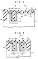
- Figs. 2 and 3 are cross sectional views taken along line II-II and line III-III in Fig. 1 and illustrate the memory cell section 10.
- a p type well region 20 and a semiconductor layer 21 of a second conductivity type or n type, are formed in a cell region defined by a field insulating film 22 formed in the p type substrate 10.
- the n ⁇ type semiconductor layer 21 constitutes one of the electrodes of the memory cell capacitor Cm.
- the two recesses 16a and 16b are formed in the p type well region 20. The way, in which the two recesses 16a and 16b are formed side by side in the well region 20, is most clearly shown in Fig. 3.
- the recesses 16a and 16b are formed by a reactive ion etching (RIE) process using an etching mask (not shown).
- the p type well region 20 is formed by ion implantation or thermal diffusion of p type impurities. Particularly, the region 20 is formed such that it has a higher impurity concentration than the impurity concentration of the p type substrate (and will hereinafter be referred to as p+ type well region).
- the shape of the p+ type well region 20 is controlled such that it will not intrude into a certain substrate region where a cell transistor Qm to be described later is formed, that is, it will exclude the transistor formation region of the substrate, as is apparent from Fig. 2.
- a gate oxide film 24a and a polycrystalline silicon layer 26, which serves as a capacitor electrode, are formed in the mentioned order on the substrate surface where the recesses 16a and 16b are formed, whereby the MOS capacitor Cm of the memory cell 10 is completed. Attention should be given to the fact that the MOS capacitor electrode 26 is provided commonly over a region other than the MOS FET regions of each memory cell and dummy cell.
- the MOS FET Qm of the memory cell 10 includes n+ type diffusion layers 28 and 30, which are formed by the ion implantation technique and serve as the source and drain, respectively, and a gate layer 32 formed on the gate oxide film 24b formed on the substrate 14.
- the gate layer 32 is formed in self-alignment to the n+ type diffusion layers 28 and 30.
- An insulating layer 34 such as a SiO2 layer for instance, is deposited on the wafer structure described above. A portion of the SiO2 layer 34 on the n+ type layer 30 is removed by a well-known technique, so that an opening is formed as a contact hole 36.
- a conductive layer 38 is formed such that it is electrically connected to the drain layer 30 of the MOS FET Qm in the portion thereof exposed in the contact hole 32.
- the conductive layer 38 serves as a bit line for the MOS FET Qm of the memory cell 10.
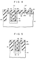
- Figs. 4 and 5 are cross sectional views taken along line IV-IV and line V-V in Fig. 1 and illustrate the dummy cell section 12.
- a p+ type well region 40 and an n type semiconductor layer 41 are formed in a dummy cell region defined by the field insulative film 22 formed in the p type substrate 10.
- the n type semiconductor layer 41 constitutes one of the electrodes of the dummy cell capacitor Cd.
- the recess 18 of the dummy cell capacitor Cd noted above, is formed in the p+ type well region 40.
- the recess 18 and p+ type well region 40 are formed in the same way as the memory cell 10 described above.
- a gate oxide film 24a and a polycrystalline silicon layer 26 which serves as a capacitor electrode are formed in the mentioned order on the substrate surface where the recess 18 is formed, thus completing the MOS capacitor Cd of the dummy cell 12.
- the MOS FET Qd of the dummy cell 12 includes n+ type diffusion layers 42 and 44 serving as the source and drain, respectively, and a gate layer 46, which is formed on the gate oxide film 24b formed on the substrate 14 in a self-aligned relationship with the n+ type diffusion layers 42 and 44.
- the insulative layer 34 such as a SiO2 layer, that is deposited on the wafer structure noted above is also partly etched away to form a contact hole 48.
- a conductive layer 50 which, serves as a bit line for the MOS FET Qd of the dummy cell 12, is electrically connected to the drain layer 44 of the MOS FET Qd in the portion thereof exposed in the contact hole 48.
- the above embodiment of the dRAM according to the invention has two recesses 16a and 16b formed in the MOS capacitor region of the memory cell 10 and one recess 18 formed in the MOS capacitor region of the dummy cell 12.
- the formation of these recesses 16a, 16b and 18 is necessary for setting the charge storage ratio of the memory cell 10 to the dummy cell 12 to 2 : 1 as is well known to persons skilled in the art.
- the capacitance ratio of the memory cell 10 to the dummy cell 12 is set to 2 : 1 with the two recesses provided for the memory cell capacitor and one recess for the dummy cell capacitor, so that an equal constant voltage may be applied as a read-out voltage to both the cells in the data read-out mode.
- the impurity concentration of the substrate region surrounding the recesses 16a and 16b is particularly increased.
- the well region 20 has the effect of suppressing or preventing the spread of the depletion layers formed around the recesses 16a and 16b with storage of charge in the cell capacitor Cd when data is stored in the cell. That is, the well region 20 can reliably prevent the depletion layers around the capacitor recesses 16a and 16b from spreading and becoming contiguous to each other in a region 20a between the two recesses 16a and 16b as shown in Fig. 3.
- the memory capacitor Cm is not formed of a single enlarged recess but of two recesses 16a and 16b of an identical rectangular planar shape, which is the same in shape and total length as the four sides of the recess 18 formed in the dummy cell 12.
- the reason for this is that the formation of the two recesses 16a and 16b in the memory cell capacitor section can equalize the rate of increase of capacitance of the dummy cell due to an error in the etching process and the rate of increase of the capacitance of the memory cell due to an error in the etching process.
- the rate of increase of the sum Lm of the total lengths of the four sides of the recesses 16a and 16b of the memory cell capacitor Cm is equal to the rate of increase of the total length of the four sides of the recess 18 of the dummy cell capacitor Cd. That is, if an error is produced in the recesses 16a, 16b and 18 in the etching process, the rate of capacitance increases (not the capacitor increase) due to the error being equal for the memory cell 10 and for the dummy cell 12.
- the aggregate side length of the recesses 16a and 16b of the MOS capacitor Cm of the memory cell 10 is also increased at double the rate of increase of the total side length of the dummy cell capacitor recess. In effect, the capacitance ratio substantially remains unchanged.
- the capacitance of the dummy cell 12 is increased with an increase of the total length Ld of the source sides of the recess 18 due to an error ⁇ L in the etching process for the formation of recesses in the substrate surface, the capacitance of the memory cell 10 will increase at a different rate from the rate of increase of the capacitance of the dummy cell 12 (i.e., at a greater rate). Therefore, the capacitance ratio between the memory cell and dummy cell will be greatly deviated from the normal ratio.
- the high impurity density well region has been formed to surround the two recesses 16a and 16b formed in the memory cell 10, such a well region is by no means limitative.
- a high impurity concentration region may be formed over the entire area inclusive of the cell transistor formation region, and then the transistor formation region may be set substantially to the same impurity density as that of the substrate. It is important that a high impurity concentration region be formed only in a cell capacitor region so that it will not extend into the cell transistor formation region. So long as this is satisfied, it is possible to suppress or prevent an undesired spread of the depletion layers around the two recesses 16a and 16b of each memory cell, which is a basic feature of the invention.
Landscapes
- Engineering & Computer Science (AREA)
- Computer Hardware Design (AREA)
- Semiconductor Memories (AREA)
Claims (7)
- Halbleiterspeicheranordnung mit einer Vielzahl von auf bzw. in einem Halbleitersubstrat (14) ausgebildeten Speicherzellen (10), wobei jede Speicherzelle umfaßt: einen Speicherzellentransistor (Qm) und einen Speicherzellenkondensator (Cm), wobei jeder Kondensator (Cm) im Substrat ausgebildete Vertiefungsmittel (16a, 16b) aufweist und jeder Kondensator (Cm) so aufladbar ist, daß er den logischen Zustand seiner (zugeordneten) Speicherzelle (10) widerspiegelt,
eine Verarmungsschichtausbreitung-Unterdrückungseinheit (20) zum Unterdrücken der Ausbreitung von Verarmungsschichten, die um die Vertiefungsmittel (16a, 16b) des Speicherzellenkondensators (Cm) herum entstehen, wenn in diesem Ladung gespeichert ist, um damit den Ladungsspeicherwirkungsgrad des Speicherzellenkondensators zu verbessern, und
eine Vielzahl von Blindzellen (12), die jeweils einen Blindzellentransistor (Qd) und einen Blindzellenkondensator (Cd) mit Vertiefungsmitteln aufweisen, wobei der Kondensator auf einen gewählten Spannungspegel voraufladbar ist,
dadurch gekennzeichnet, daß die Vertiefungsmittel zwei erste Vertiefungen oder Ausnehmungen (16a, 16b) umfassen, während die Vertiefungsmittel des Blindzellenkondensators (Cd) eine weitere Vertiefung oder Ausnehmung (18) aufweisen, wobei die ersten Vertiefungen und die weitere Vertiefung im wesentlichen gleiche Größe besitzen, so daß ein Kapazitätsverhältnis von 2:1 zwischen dem Speicherzellenkondensator (Cm) und dem Blindzellenkondensator (Cd) mit verbesserter Genauigkeit steuerbar bzw. einstellbar ist. - Anordnung nach Anspruch 1, dadurch gekennzeichnet, daß die Verarmungsschichtausbreitung-Unterdrückungseinheit eine die beiden ersten Vertiefungen des Speicherzellenkondensators unter Ausschuß des Speicherzellentransistors umgebende Halbleiterzone (20) des gleichen Leitungstyps wie das Substrat umfaßt und die Halbleiterzone (20) eine höhere Fremdatomkonzentration als das Substrat (14) aufweist.
- Anordnung nach Anspruch 2, dadurch gekennzeichnet, daß die Halbleiterzone eine im Substrat (14) in der Weise ausgebildete Wannenzone (20) umfaßt, daß die beiden ersten Vertiefungen des Speicherzellenkondensators innerhalb der Wannenzone (20) liegen.
- Anordnung nach Anspruch 3, dadurch gekennzeichnet, daß die Summe der Längen der Umfänge der beiden Vertiefungen (16a, 16b) jedes Speicherzellenkondensators das Doppelte der Umfangslänge der Vertiefung (18) des Blindzellenkondensators beträgt, so daß in einem Ätzprozeß zur Ausbildung der ersten Vertiefungen (16a, 16b) und der weiteren Vertiefung (18), die jeweils die Speicherzellenkapazität bzw. die Blindzellenkapazität bestimmen, auch dann, wenn sich die planaren Formen aufgrund von Ätzfertigungsfehlern ändern, das Umfangslängenverhältnis der ersten Vertiefungen (16a, 16b) zur weiteren Vertiefung (18) nach der Bearbeitung konstant ist, so daß das Kapazitätsverhältnis der ersten Vertiefungen (16a, 16b) zur weiteren Vertiefung (18) mit einer vorbestimmten Größe übereinstimmt.
- Anordnung nach Anspruch 4, dadurch gekennzeichnet, daß die ersten Vertiefungen (16a, 16b) und die weitere Vertiefung (18) mittels des gleichen Ätzprozesses gleichzeitig am bzw. im Substrat ausgebildet werden, so daß sie jeweils gleiche Tiefe aufweisen.
- Anordnung nach Anspruch 5, dadurch gekennzeichnet, daß jede der ersten Vertiefungen (16a, 16b) die gleiche planare Form wie die planare Form der weiteren Vertiefung (18) aufweist.
- Anordnung nach Anspruch 6, dadurch gekennzeichnet, daß die ersten Vertiefungen (16a, 16b) und die weitere Vertiefung (18) jeweils eine rechteckige planare Form aufweisen.
Applications Claiming Priority (2)
| Application Number | Priority Date | Filing Date | Title |
|---|---|---|---|
| JP62728/84 | 1984-03-30 | ||
| JP59062728A JPS60206163A (ja) | 1984-03-30 | 1984-03-30 | 半導体記憶装置 |
Publications (3)
| Publication Number | Publication Date |
|---|---|
| EP0159824A2 EP0159824A2 (de) | 1985-10-30 |
| EP0159824A3 EP0159824A3 (en) | 1987-04-01 |
| EP0159824B1 true EP0159824B1 (de) | 1992-01-15 |
Family
ID=13208712
Family Applications (1)
| Application Number | Title | Priority Date | Filing Date |
|---|---|---|---|
| EP85302109A Expired EP0159824B1 (de) | 1984-03-30 | 1985-03-26 | Halbleiterbauelement mit versenktem Kondensator |
Country Status (4)
| Country | Link |
|---|---|
| EP (1) | EP0159824B1 (de) |
| JP (1) | JPS60206163A (de) |
| KR (1) | KR900005664B1 (de) |
| DE (1) | DE3585173D1 (de) |
Families Citing this family (10)
| Publication number | Priority date | Publication date | Assignee | Title |
|---|---|---|---|---|
| KR930007522B1 (ko) * | 1985-03-08 | 1993-08-12 | 가부시끼 가이샤 히다찌세이사꾸쇼 | 종형 커패시터를 사용한 반도체메모리 |
| US4751558A (en) * | 1985-10-31 | 1988-06-14 | International Business Machines Corporation | High density memory with field shield |
| JPS62120070A (ja) * | 1985-11-20 | 1987-06-01 | Toshiba Corp | 半導体記憶装置 |
| JPS63122261A (ja) * | 1986-11-12 | 1988-05-26 | Mitsubishi Electric Corp | 半導体装置の製造方法 |
| US5260226A (en) * | 1987-07-10 | 1993-11-09 | Kabushiki Kaisha Toshiba | Semiconductor device having different impurity concentration wells |
| DE3855945T2 (de) * | 1987-07-10 | 1997-11-13 | Toshiba Kawasaki Kk | Halbleiterbauelement mit Bereichen unterschiedlicher Störstellenkonzentration |
| US5726475A (en) * | 1987-07-10 | 1998-03-10 | Kabushiki Kaisha Toshiba | Semiconductor device having different impurity concentration wells |
| KR910000246B1 (ko) * | 1988-02-15 | 1991-01-23 | 삼성전자 주식회사 | 반도체 메모리장치 |
| US4918454A (en) * | 1988-10-13 | 1990-04-17 | Crystal Semiconductor Corporation | Compensated capacitors for switched capacitor input of an analog-to-digital converter |
| US5208597A (en) * | 1988-10-13 | 1993-05-04 | Crystal Semiconductor | Compensated capacitors for switched capacitor input of an analog-to-digital converter |
Family Cites Families (2)
| Publication number | Priority date | Publication date | Assignee | Title |
|---|---|---|---|---|
| JPS57186354A (en) * | 1981-05-13 | 1982-11-16 | Hitachi Ltd | Semiconductor memory storage and manufacture thereof |
| JPS58137245A (ja) * | 1982-02-10 | 1983-08-15 | Hitachi Ltd | 大規模半導体メモリ |
-
1984
- 1984-03-30 JP JP59062728A patent/JPS60206163A/ja active Pending
- 1984-10-19 KR KR1019840006508A patent/KR900005664B1/ko not_active Expired
-
1985
- 1985-03-26 DE DE8585302109T patent/DE3585173D1/de not_active Expired - Lifetime
- 1985-03-26 EP EP85302109A patent/EP0159824B1/de not_active Expired
Also Published As
| Publication number | Publication date |
|---|---|
| JPS60206163A (ja) | 1985-10-17 |
| EP0159824A2 (de) | 1985-10-30 |
| KR900005664B1 (ko) | 1990-08-03 |
| KR850006981A (ko) | 1985-10-25 |
| DE3585173D1 (de) | 1992-02-27 |
| EP0159824A3 (en) | 1987-04-01 |
Similar Documents
| Publication | Publication Date | Title |
|---|---|---|
| KR100200222B1 (ko) | 반도체 장치와 그 제조방법 | |
| US4907047A (en) | Semiconductor memory device | |
| JP3423128B2 (ja) | 側壁静電容量体dramセル | |
| US5220530A (en) | Semiconductor memory element and method of fabricating the same | |
| EP0176254B1 (de) | Halbleiterspeichervorrichtung | |
| EP0241948B1 (de) | Halbleiterspeicher und sein Herstellungsverfahren | |
| US5317178A (en) | Offset dual gate thin film field effect transistor | |
| US6888187B2 (en) | DRAM cell with enhanced SER immunity | |
| US4894695A (en) | Semiconductor device with no stress generated at the trench corner portion and the method for making the same | |
| KR900000170B1 (ko) | 다이내믹형 메모리셀과 그 제조방법 | |
| US4855953A (en) | Semiconductor memory device having stacked memory capacitors and method for manufacturing the same | |
| KR920010193B1 (ko) | 금속 절연물 반도체형 다이나믹 랜덤 액세스 메모리 장치 | |
| JPH04188869A (ja) | 接合型電界効果トランジスタとキャパシタとを含む半導体記憶装置およびその製造方法 | |
| US4918500A (en) | Semiconductor device having trench capacitor and manufacturing method therefor | |
| EP0159824A2 (de) | Halbleiterbauelement mit versenktem Kondensator | |
| US4613883A (en) | Dynamic semiconductor memory cell and method for its manufacture | |
| US6265748B1 (en) | Storage cell arrangement in which vertical MOS transistors have at least three different threshold voltages depending on stored data, and method of producing said arrangement | |
| KR910002038B1 (ko) | 반도체 기억장치 | |
| US5258321A (en) | Manufacturing method for semiconductor memory device having stacked trench capacitors and improved intercell isolation | |
| US5200353A (en) | Method of manufacturing a semiconductor device having trench capacitor | |
| JPS6136384B2 (de) | ||
| US6028361A (en) | Method of manufacturing of semiconductor device having low leakage current | |
| JPH03205867A (ja) | 半導体記憶装置 | |
| JPH0744226B2 (ja) | 半導体装置及びその製造方法 | |
| US5329148A (en) | Semiconductor device and preparing method therefor |
Legal Events
| Date | Code | Title | Description |
|---|---|---|---|
| PUAI | Public reference made under article 153(3) epc to a published international application that has entered the european phase |
Free format text: ORIGINAL CODE: 0009012 |
|
| 17P | Request for examination filed |
Effective date: 19850411 |
|
| AK | Designated contracting states |
Designated state(s): DE FR GB |
|
| PUAL | Search report despatched |
Free format text: ORIGINAL CODE: 0009013 |
|
| AK | Designated contracting states |
Kind code of ref document: A3 Designated state(s): DE FR GB |
|
| 17Q | First examination report despatched |
Effective date: 19891010 |
|
| GRAA | (expected) grant |
Free format text: ORIGINAL CODE: 0009210 |
|
| AK | Designated contracting states |
Kind code of ref document: B1 Designated state(s): DE FR GB |
|
| REF | Corresponds to: |
Ref document number: 3585173 Country of ref document: DE Date of ref document: 19920227 |
|
| PG25 | Lapsed in a contracting state [announced via postgrant information from national office to epo] |
Ref country code: FR Effective date: 19920605 |
|
| EN | Fr: translation not filed | ||
| PLBE | No opposition filed within time limit |
Free format text: ORIGINAL CODE: 0009261 |
|
| STAA | Information on the status of an ep patent application or granted ep patent |
Free format text: STATUS: NO OPPOSITION FILED WITHIN TIME LIMIT |
|
| 26N | No opposition filed | ||
| REG | Reference to a national code |
Ref country code: FR Ref legal event code: ST |
|
| PGFP | Annual fee paid to national office [announced via postgrant information from national office to epo] |
Ref country code: GB Payment date: 19970317 Year of fee payment: 13 |
|
| PG25 | Lapsed in a contracting state [announced via postgrant information from national office to epo] |
Ref country code: GB Free format text: LAPSE BECAUSE OF NON-PAYMENT OF DUE FEES Effective date: 19980326 |
|
| GBPC | Gb: european patent ceased through non-payment of renewal fee |
Effective date: 19980326 |
|
| PGFP | Annual fee paid to national office [announced via postgrant information from national office to epo] |
Ref country code: DE Payment date: 20040408 Year of fee payment: 20 |