EP0159893B1 - Signalgeneratorschaltungen - Google Patents
Signalgeneratorschaltungen Download PDFInfo
- Publication number
- EP0159893B1 EP0159893B1 EP85302625A EP85302625A EP0159893B1 EP 0159893 B1 EP0159893 B1 EP 0159893B1 EP 85302625 A EP85302625 A EP 85302625A EP 85302625 A EP85302625 A EP 85302625A EP 0159893 B1 EP0159893 B1 EP 0159893B1
- Authority
- EP
- European Patent Office
- Prior art keywords
- signal
- clk
- voltage
- display clock
- controlled oscillator
- Prior art date
- Legal status (The legal status is an assumption and is not a legal conclusion. Google has not performed a legal analysis and makes no representation as to the accuracy of the status listed.)
- Expired - Lifetime
Links
Images


Classifications
-
- H—ELECTRICITY
- H04—ELECTRIC COMMUNICATION TECHNIQUE
- H04N—PICTORIAL COMMUNICATION, e.g. TELEVISION
- H04N5/00—Details of television systems
- H04N5/44—Receiver circuitry for the reception of television signals according to analogue transmission standards
- H04N5/445—Receiver circuitry for the reception of television signals according to analogue transmission standards for displaying additional information
- H04N5/44504—Circuit details of the additional information generator, e.g. details of the character or graphics signal generator, overlay mixing circuits
Definitions
- This invention relates to signal generator circuits. More particularly, but not exclusively, the invention relates to a signal generator circuit for generating a synchronisation signal, a display clock signal and similar signals for a television receiver employed in a character and picture image information system such as a CAPTAIN ( c haracter a nd p attern t elephone a ccess i nformation n etwork) or other videotex system and which uses, for example, a telephone network line for signal transmission.
- a character and picture image information system such as a CAPTAIN ( c haracter a nd p attern t elephone a ccess i nformation n etwork) or other videotex system and which uses, for example, a telephone network line for signal transmission.
- signals such as vertical and horizontal synchronisation signals, a colour sub-carrier signal (for example, a signal having a frequency of substantially 3.58 MHz) and a display clock signal (for example, a signal having a frequency of substantially 5.727 MHz).
- a colour sub-carrier signal for example, a signal having a frequency of substantially 3.58 MHz
- a display clock signal for example, a signal having a frequency of substantially 5.727 MHz.
- the position of the special pulse is determined by the operation of a counter which begins at a time which, because of deficiencies in previously proposed structures, may change by one clock period in successive horizontal lines. This of course correspondingly displaces the display position pulse so that a jitter appears in the horizontal direction in a picture reproduced on the screen of the television receiver.
- a signal generator circuit comprising: reference signal oscillator means for producing a square-wave reference signal having a series of rising edges; means responsive to the reference signal for generating a horizontal synchronisation signal synchronised with the reference signal; frequency-dividing means responsive to the reference signal for producing a square-wave colour sub-carrier signal having a series of rising edges; a phase-locked loop circuit responsive to the sub-carrier signal and including a voltage-controlled oscillator, the voltage-controlled oscillator being operative to produce a square-wave oscillation signal having a series of rising edges, at least one rising edge of the sub-carrier signal coinciding with a rising edge of the oscillation signal from the voltage-controlled oscillator, the oscillation signal from the voltage-controlled oscillator being synchronised with the sub-carrier signal (SC); means for detecting a time at which a rising edge of the sub-carrier signal coincides with a rising edge of the oscillation signal of the voltage-controlled oscillator; means for generating a square
- a preferred signal generator circuit embodying the invention and described hereinbelow can generate a synchronisation signal for a television receiver for use with a CAPTAIN or other videotex character and picture information system and similar systems.
- a display position pulse is formed at a constant position with respect to a horizontal synchronisation signal so that jitter in the horizontal direction of a picture displayed on a screen can be avoided.
- the preferred signal generator circuit can produce a display clock signal and a horizontal synchronisation signal having a constant phase relation therebetween such that, for example, the rising edge of the display clock signal and the rising edge of the horizontal synchronisation avoid coincidence with each.
- Figure 1 shows a typical previously proposed signal generator circuit for generating a colour sub-carrier signal and a display clock signal for use in a television receiver forming part of a CAPTAIN or other videotex system or the like.
- an oscillator circuit 1 generates an oscillation signal with a frequency of substantially 14.32 MHz, which is four times the desired colour sub-carrier frequency of substantially 3.58 MHz.
- the oscillation signal is supplied to a television synchronisation signal generator circuit 2, which produces a vertical synchronization signal P V and a horizontal synchronisation signal P H .
- the oscillation signal of 14.32 MHz from the oscillator circuit 1 is supplied also to a frequency divider 3, which divides the input frequency of 14.32 MHz by four to produce the colour sub-carrier signal SC of 3.58 MHz.
- the colour sub-carrier signal SC is utilised in a known manner by circuitry not shown. Since the horizontal synchronisation signal P H and the colour sub-carrier signal SC are produced in response to the same oscillation signal from the oscillator circuit 1, they are synchronised with each other in phase.
- the colour sub-carrier signal SC of 3.58 MHz from the frequency divided 3 is supplied also to a frequency divider 4, which divides the input frequency of 3.58 MHz by five and supplies a signal having a frequency of substantially 716 KHz to a phase comparator 5.
- a voltage-controlled oscillator (VCO) 6 generates a signal having a frequency of substantially 11.454 MHz. This signal is supplied to a frequency divider 7 that divides by two. An output of the divider 7 is supplied to a frequency divider 8 that divides by eight. An output of the frequency divider 8 is supplied to the phase comparator 5 in which it is compared in phase with the signal of substantially 716 KHz which results from frequency-dividing the colour sub-carrier signal SC of 3.58 MHz by five. An error signal from the phase comparator 5 is supplied through a low-pass filter 9 to the voltage-controlled oscillator 6 as a control voltage thereof.
- the voltage-controlled oscillator 6 produces an oscillation signal of substantially 11.454 MHz and the frequency divider 7 produces a signal of substantially 5.727 MHz which is supplied to circuitry (not shown) as a display clock signal CLK.
- the display clock signal CLK is, of course, synchronised in phase with the colour sub-carrier signal SC.
- the frequency (5.727 MHz) of the display clock signal CLK is thus 8/5 times the frequency (3.58 MHz) of the colour sub-carrier signal SC.
- Phase synchronisation is established between the signal obtained by frequency-dividing the colour sub-carrier signal SC by five (by means of the divider 4) and that obtained by frequency-dividing the display clock signal CLK by eight (by means of the divider 8).
- the phase difference between the display clock signal CLK (shown in line A of Figure 2) and the colour sub-carrier signal SC (shown in line B of Figure 2) assumes five different values at the times P1 to P5.
- each of the times P1 to P5 coincides with a rising edge of the colour sub-carrier signal SC, but only the time P1 coincides with a rising edge of the display clock signal CLK; the remaining times P2 to P5 fall varying distances between rising and falling edges of the display clock signal CLK. Since, as indicated above, the horizontal synchronisation signal P H is phase-synchronised with the colour sub-carrier signal SC, the phase difference between the respective rising edges of the horizontal synchronisation signal P H and the display clock signal CLK also assumes any of five different values at times P1 to P5, as shown in line A in conjunction with lines C to G of Figure 2.
- the one of the times P1 to P5 at which the phase difference between the rising edges of the horizontal synchronisation signal P H and the display clock signal CLK is measured is randomly determined in accordance with the initial state of a counter or the like included in the synchronisation signal generator circuit 2 and the lock-in time of a phase-locked loop (PLL) circuit that includes the phase comparator 5, the voltage-controlled oscillator 6, etc.
- PLL phase-locked loop
- the display position in the horizontal direction is determined with reference to the horizontal synchronisation signal P H : that is, such information is displayed at a predetermined position (time) with respect to the position (time) of the horizontal synchronisation signal P H .
- a special pulse hereinafter referred to as a display position pulse
- the display position pulse is generated by employing the rising edge of the horizontal synchronisation signal P H to reset (or preset) a counter or the like (not shown) and by then counting the successive rising edges of the display clock signal CLK until a count value is reached which corresponds to the desired display position.
- the phase difference between the rising edges of the horizontal synchronisation signal P H and the display clock signal CLK will assume any of five values respectively indicated at the times P1 to P5. If the randomly-determined time is such that the rising edge of the horizontal synchronisation signal P H and the rising edge of the display clock signal CLK are very close to each other, as at the time P1, then when the rising edge of the horizontal synchronisation signal P H appears, it becomes difficult to determine whether the count of the display clock signal CLK pulses should begin with the present or instant rising edge thereof or whether it should begin with the next following rising edge thereof. As a result, in the worst case, the operation of the counter begins at a time which changes by one clock period at every horizontal line. This of course correspondingly displaces the display position pulse. Thus, a jitter appears in the horizontal direction in a picture reproduced on the screen of the television receiver. Statistically, the horizontal jitter is unlikely to affect every line, but occurs periodically.
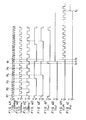
- FIGS 3 and 4A to 4I illustrate a preferred embodiment of signal generator circuit according to the present invention which reliably prevents horizontal jitter in the display.
- the display clock signal CLK ( Figure 4H) and the horizontal synchronisation signal P H ( Figure 4I) always have a constant phase relation therebetween in which the rising edge of the display clock signal CLK and the rising edge of the horizontal synchronisation signal P H never coincide with each other.
- a falling edge of the display clock signal CLK coincides with the rising edge of the horizontal synchronisation signal P H , as shown in Figures 4H and 4I at a time t3.
- a television synchronisation signal generator circuit 2' has a clock input terminal CK to which an oscillation signal having a frequency of substantially 14.32 MHz is supplied from the oscillator 1. On the basis of the oscillation signal of 14.32 MHz supplied thereto, the synchronisation signal generator circuit 2' produces a vertical synchronisation signal P V and a horizontal synchronisation signal P H .
- the circuit 2' includes a reset terminal R. When a low-level signal "0" is supplied to the reset terminal R, the circuit 2' is held in a reset state; and, when a high-level signal "1" is supplied to the reset terminal R, the circuit 2' starts its operation.
- the oscillation signal of 14.32 MHz from the oscillator 1 is supplied also to a frequency divider 3, which divides the 14.32 MHz signal by four and produces a colour sub-carrier signal SC having a frequency of substantially 3.58 MHz.
- the colour sub-carrier signal SC is supplied to a frequency divider 4, which divides the 3.58 MHz signal by five and produces a signal having a frequency of substantially 716 KHz.
- the output of the frequency divider 4 is supplied to a phase comparator 5.
- the frequency divider 10 divides the frequency of the signal from the VCO 6 by sixteen and supplies an output to the phase comparator 5.
- the frequency divider 10 like the other frequency dividers employed in the present signal generator circuit, may comprise a counter.
- the divider 10 may comprise, for example, an up-mode counter for counting from 0 to 15 and producing one output pulse for every sixteen input pulses.
- the phase comparator 5 makes a phase comparison between the signal supplied by the divider 10 and the above-mentioned signal which is generated by the frequency divider 4 when it divides the frequency of the colour sub-carrier signal SC of 3.58 MHz by five.
- the compared error signal from the phase comparator 5 is supplied through a low-pass filter (LPF) 9 to the VCO 6 as its control voltage so that the VCO 6 produces an oscillation signal CLK0 (shown in Figure 4A) of substantially 11.454 MHz.
- LPF low-pass filter
- the oscillation signal CLK0 from the VCO 6 is supplied to a timer circuit 11.
- the oscillation signal CLK0 supplied thereto is counted.
- the timer 11 produces a low-level signal "0" at its output; thereafter, the timer 11 produces a high-level signal "1" at its output.
- the output signal from the timer 11 is supplied to one input terminal of an AND gate 12.
- a detecting circuit 13 is provided to detect a time P1 at which the rising edge of the colour sub-carrier signal SC of 3.58 MHz (shown in Figure 4C) coincides with the rising edge of the oscillation signal CLK0 of 11.454 MHz (shown in Figure 4A).
- the detecting circuit 13 is supplied with signals corresponding to selected bits of a counter incorporated in the frequency divider 10 so that the detecting circuit 13 produces a signal S M which, as shown in Figure 4F, becomes high or "1" during each period of the signal CLK0 in which the count value of such counter is maximum.
- the signal S M goes high during the period of the signal CLK0 in which the count value of the counter is minimum.
- the maximum or minimum count is reached during the period of the signal CLK0 immediately preceding the time P1.
- the detection signal S M is high or "1" during the interval from t0 to t1 and is supplied to another input terminal of the AND gate 12.
- the K input terminal of the flip-flop 14 is grounded, and a clock input terminal CK thereof is supplied with the oscillation signal CLK0.
- the signal obtained at the junction or connection point P between the resistor 16 and the capacitor 17 is supplied to a clear terminal CLR of the flip-flop 14.
- the signal produced at the junction P is low or "0" during a predetermined period T0 (determined by the time constant of the resistor 16 and the capacitor 17) after power is applied to the terminal 15.
- a signal S Q (shown in Figures 3 and 4G) obtained at the output terminal Q of the flip-flop 14 is supplied to the reset terminal R of the synchronisation signal generator 2'.
- the signal S Q is also supplied to a clear terminal CLR of a D-type flip-flop 18.
- the flip-flop 18 receives the oscillation signal CLK0 (shown in Figures 3 and 4A) from the VCO 6 at a clock input terminal CK thereof so that the flip-flop 18 is operated at each rising edge of the oscillation signal CLK0.
- the signal obtained in response thereto at an inverted output terminal Q of the flip-flop 18 is supplied to a D input terminal thereof so that the flip-flop 18 produces the display clock signal CLK ( Figures 3 and 4H) of substantially 5.727 MHz at an output terminal Q.
- Figure 4B shows the display clock signal CLK of Figure 1 and line A of Figure 2 which is reproduced in Figure 4B. It is evident that the display clock signal CLK in Figure 4B is 180 o out of phase with that of Figure 4H.
- Figure 4D shows the output signal from the frequency divider 10 which is supplied to the phase comparator 5
- Figure 4E shows the output signal from the frequency divider 4, which is likewise supplied to the phase comparator 5.
- the above-described signal generator circuit embodying the invention operates as follows.
- the flip-flop 18 holds its clear mode during the period T0 (see the lefthand portion of Figure 4G) and thus the display clock signal CLK is not produced at the output terminal Q thereof (see the lefthand portion of Figure 4H).
- the timer circuit 11 After the phase-locked loop (PLL) circuit including the VCO 6 stabilises, the timer circuit 11 produces an output signal which is high or "1" and which is supplied to one input terminal of the AND gate 12.
- the detecting circuit 13 produces the signal S M as shown in Figures 3 and 4F, and the signal S M is supplied to the other input terminal of the AND gate 12. Accordingly, during the period from t0 to t1 in which the detection signal S M is high or "1", the AND gate 12 produces at its output a signal which is high or "1", and this output is supplied to the J terminal of the flip-flop 14.
- the signal S Q (shown in Figures 3 and 4G) produced at the output terminal Q of the flip-flop 14 is changed from low or "0" to high or "1" at the time t1. Since the K terminal of the flip-flop 14 is grounded, the flip-flop 14 remains in the high or "1" state after the time t1.
- the signal S Q which is now high or "1" is supplied to the reset terminal R of the synchronisation signal generator 2' and to the clear terminal CLR of the flip-flop 18.
- the circuit 2' starts its operation and the clear mode of the flip-flop 18 is released.
- the display clock signal CLK (shown in Figures 3 and 4H) of substantially 5.727 MHz is produced at its output terminal Q beginning at the time t2, which follows the time t1 by one period of the signal CLK0.
- the position at which the display position pulse is formed is always constant (that is, it never fluctuates). As a result, horizontal jitter in the displayed picture is prevented.
- the signal generator circuit embodying the invention is thus ideally suited for a television receiver for use with a CAPTAIN or other videotex character and picture information system and similar systems.
- a display position pulse is formed at a constant position so that jitter in the horizontal direction of a picture displayed on a screen is avoided.
- the signal generator circuit embodying the invention can produce a display clock signal and a horizontal synchronisation signal having a constant phase relation therebetween such that, for example, the rising edge of the display clock signal and the rising edge of the horizontal synchronisation signal are never coincident with each other.
- phase relationship between the rising edge of the display clock signal CLK and the rising edge of the horizontal synchronisation signal P H can be varied parametrically so long as they are never selected so that they coincide.
- frequencies of the various signals and, correspondingly, the characteristics of the oscillators and frequency dividers can be varied.
- devices other than the disclosed detector, dividers, oscillator and flip-flops can be used for generating the signals S M , S Q , CLK0 and CLK.
Landscapes
- Engineering & Computer Science (AREA)
- Computer Graphics (AREA)
- Multimedia (AREA)
- Signal Processing (AREA)
- Synchronizing For Television (AREA)
- Controls And Circuits For Display Device (AREA)
- Stabilization Of Oscillater, Synchronisation, Frequency Synthesizers (AREA)
Claims (7)
- Signalgenerator-Schaltkreis mit:
einem Referenzsignal-Oszillator (1) zur Erzeugung eines Rechteckwellen-Referenzsignals mit einer Folge von Anstiegsflanken;
einem Schaltungsteil (2'), das auf das Referenzsignal mit Erzeugen eines Zeilen-Synchronsignals (PH) anspricht, das mit dem Referenzsignal synchronisiert ist;
einem Frequenzteiler (3), der auf das Referenzsignal anspricht und ein Rechteckwellen-Farb-Subträgersignal (SC) erzeugt, das eine Folge von Anstiegsflanken hat;
einer Phasenregelschleife, die auf das Subträgersignal (SC) anspricht und die einen spannungsgesteuerten-Oszillator (6) hat, wobei der spannungsgesteuerte Oszillator dazu vorgesehen ist, ein Rechteckwellen-Oszillatorsignal (CLK₀) zu erzeugen, das eine Folge von Anstiegsflanken hat, wobei wenigstens eine der Anstiegsflanken des Subträgersignals (SC) mit einer Anstiegsflanke des Oszillatorsignals (CLK₀) des spannungsgesteuerten Oszillators (6) koinzidiert, wobei das Oszillatorsignal (CLK₀) des spannungsgesteuerten Oszillators (6) mit dem Subträgersignal (SC) synchronisiert ist;
einer Detektorschaltung (13) zur Detektion eines Zeitpunktes, zu dem eine Anstiegsflanke des Subträgersignals (SC) mit einer Anstiegsflanke des Oszillatorsignals (CLK₀) des spannungsgesteuerten Oszillators koinzidiert;
einer Generatorschaltung (18) zur Erzeugung eines Rechteckwellen-Display-Taktsignals (CLK), das mit dem Oszillatorsignal (CLK₀) des spannungsgesteuerten Oszillators (6) synchronisiert ist und eine Folge von Rückflanken hat;
einem Generatorteil Zur Erzeugung einer Versorgungsspannung für den Signalgenerator, wobei die Versorgungsspannung auf einen stabilen Wert (+B) in einem vorgegebenen Zeitraum (T₀) nach Anliegen der Spannungsversorgung an dem Generatorteil ansteigt;
einer Detektorschaltung zur Detektion des Anstiegs der Versorgungsspannung;
wobei die Detektorschaltung (13) zur Zeitdetektion und die Detektorschaltung zur Detektion des Anstiegs die Phasen des Schaltungsteils (2') zur Erzeugung des Zeilen-Synchronsignals und die Generatorschaltung (18) für das Display-Taktsignal steuert, um eine Phasenbeziehung zu haben, bei der die Anstiegsflanke des Zeilen-Synchronsignals (PH) nicht mit der Anstiegsflanke des Display-Taktsignals (CLK) koinzidiert. - Signal-Generator-Schaltkreis nach Anspruch 1,
bei dem die Detektorschaltung (13) zur Detektion eines Zeitpunktes und die Detektorschaltung für den Anstieg die Phasen des Schaltungsteils (2') zur Erzeugung eines Zeilen-Synchronsignals und die Generatorschaltung (18) für die Erzeugung des Display-Taktsignals steuert, um eine Phasenbeziehung zu haben, bei der die Anstiegsflanke des Zeilen-Synchronsignals (PH) mit einer Rückflanke des Display-Taktsignals (CLK) koinzidiert. - Signal-Generator-Schaltkreis nach Anspruch 1 oder 2,
mit einem Schaltungsteil (14) zur Bestimmung eines Zeitpunktes für den Start des Schaltungsteils (2') zur Erzeugung eines Zeilen-Synchronsignals und der Generatorschaltung (18) zur Erzeugung des Display-Taktsignals, wobei dieser Schaltungsteil (14) für das Starten von der Detektorschaltung (13) zur Detektion eines Zeitpunktes und der Detektorschaltung für den Anstieg gesteuert wird. - Signal-Generator-Schaltkreis nach Anspruch 3,
mit einem Schaltungsteil (11) zur Detektion des Zustands der Phasenregelschleife, wobei ein Ausgangssignal dieses Schaltungseils (11) dem Schaltungsteil (14) für das Starten zugeführt wird. - Signal-Generator-Schaltkreis nach Anspruch 4,
mit einer UND-Schaltung (12), die auf die Detektorschaltung (13) zur Detektion eines Zeitpunktes und das Schaltungsteil (11) zur Detektion des Zustands der Phasenregelschleife anspricht und ein Ausgangssignal an das Schaltungsteil (14) für das Starten liefert. - Signal-Generator-Schaltkreis nach Anspruch 3 oder 4 oder 5,
bei dem die Generatorschaltung (18) zur Erzeugung des Display-Taktsignals und das Schaltungsteil (14) für das Starten jeweils Flip-Flop-Schaltkreise haben, die so verbunden sind, daß ihnen das Oszillatorsignal (CLK₀) des spannungsgesteuerten Oszillators (6) zugeführt wird. - Signal-Generator-Schaltkreis nach Anspruch 6,
bei dem das Oszillatorsignal (CLK₀) des spannungsgesteuerten Oszillators (6) periodisch ist und die Generatorschaltung (18) zur Erzeugung des Display-Taktsignals ein D-Flip-Flop (18) mit einem Eingangsanschluß (D) und einem invertierten Ausgangsanschluß (Q ), die miteinander verbunden sind, und einem anderen Eingangsanschluß (CK) hat, dem das Oszillatorsignal (CLK₀) des spannungsgesteuerten Oszillators (6) zugeführt wird, so daß die Generatorschaltung zur Erzeugung des Display-Taktsignals mit der Erzeugung des Display-Taktsignals (CLK) während der Zeitdauer des Oszillatorsignals (CLK₀) des spannungsgesteuerten Oszillators unmittelbar auf den Startzeitpunkt folgend beginnt.
Applications Claiming Priority (2)
| Application Number | Priority Date | Filing Date | Title |
|---|---|---|---|
| JP74365/84 | 1984-04-13 | ||
| JP59074365A JPH0644818B2 (ja) | 1984-04-13 | 1984-04-13 | 表示装置 |
Publications (3)
| Publication Number | Publication Date |
|---|---|
| EP0159893A2 EP0159893A2 (de) | 1985-10-30 |
| EP0159893A3 EP0159893A3 (en) | 1988-07-27 |
| EP0159893B1 true EP0159893B1 (de) | 1993-01-20 |
Family
ID=13545053
Family Applications (1)
| Application Number | Title | Priority Date | Filing Date |
|---|---|---|---|
| EP85302625A Expired - Lifetime EP0159893B1 (de) | 1984-04-13 | 1985-04-15 | Signalgeneratorschaltungen |
Country Status (6)
| Country | Link |
|---|---|
| US (1) | US4617594A (de) |
| EP (1) | EP0159893B1 (de) |
| JP (1) | JPH0644818B2 (de) |
| AU (1) | AU581883B2 (de) |
| CA (1) | CA1248596A (de) |
| DE (1) | DE3587002T2 (de) |
Families Citing this family (10)
| Publication number | Priority date | Publication date | Assignee | Title |
|---|---|---|---|---|
| US4769704A (en) * | 1985-06-04 | 1988-09-06 | Matsushita Electric Industrial Co., Ltd. | Synchronization signal generator |
| US4970596A (en) * | 1988-09-07 | 1990-11-13 | North American Philips Corp. | Pseudo line locked write clock for picture-in-picture video applications |
| AU618411B2 (en) * | 1988-10-13 | 1991-12-19 | Sony Corporation | Flicker reduction apparatus |
| KR0157585B1 (ko) * | 1993-09-24 | 1998-12-15 | 김광호 | 디스크재생장치의 동기내삽회로 및 동기상태검출회로 |
| JP3846735B2 (ja) * | 1994-12-06 | 2006-11-15 | フィリップス エレクトロニクス ネムローゼ フェン ノートシャップ | 垂直位置−ジッタ除去 |
| US5675273A (en) * | 1995-09-08 | 1997-10-07 | International Business Machines Corporation | Clock regulator with precision midcycle edge timing |
| JP3879951B2 (ja) * | 1997-09-02 | 2007-02-14 | ソニー株式会社 | 位相調整装置、位相調整方法及び表示装置 |
| JP2000305655A (ja) | 1999-04-19 | 2000-11-02 | Mitsubishi Electric Corp | 周波数逓倍回路内蔵のマイクロコンピュータ |
| US10439754B2 (en) | 2016-04-13 | 2019-10-08 | The Boeing Company | Methods and apparatus to implement a third-order signal scrambler |
| US10476708B2 (en) | 2016-04-13 | 2019-11-12 | The Boeing Company | Methods and apparatus to implement a signal scrambler |
Family Cites Families (6)
| Publication number | Priority date | Publication date | Assignee | Title |
|---|---|---|---|---|
| GB1593424A (en) * | 1977-09-26 | 1981-07-15 | Philips Electronic Associated | Television receiver arrangement |
| JPS6033030B2 (ja) * | 1978-12-23 | 1985-07-31 | ソニー株式会社 | 同期信号発生器 |
| US4464679A (en) * | 1981-07-06 | 1984-08-07 | Rca Corporation | Method and apparatus for operating a microprocessor in synchronism with a video signal |
| JPS5871784A (ja) * | 1981-10-26 | 1983-04-28 | Hitachi Ltd | 固体カラ−ビデオカメラの同期信号発生回路 |
| JPS58111977A (ja) * | 1981-12-25 | 1983-07-04 | ソニー株式会社 | カラ−表示回路 |
| JPS58191573A (ja) * | 1982-05-06 | 1983-11-08 | Victor Co Of Japan Ltd | 水平走査周波数逓倍回路 |
-
1984
- 1984-04-13 JP JP59074365A patent/JPH0644818B2/ja not_active Expired - Lifetime
-
1985
- 1985-04-10 AU AU40973/85A patent/AU581883B2/en not_active Ceased
- 1985-04-12 US US06/722,355 patent/US4617594A/en not_active Expired - Lifetime
- 1985-04-12 CA CA000478972A patent/CA1248596A/en not_active Expired
- 1985-04-15 DE DE8585302625T patent/DE3587002T2/de not_active Expired - Lifetime
- 1985-04-15 EP EP85302625A patent/EP0159893B1/de not_active Expired - Lifetime
Also Published As
| Publication number | Publication date |
|---|---|
| JPS60217779A (ja) | 1985-10-31 |
| DE3587002T2 (de) | 1993-07-22 |
| AU4097385A (en) | 1985-10-17 |
| DE3587002D1 (de) | 1993-03-04 |
| EP0159893A3 (en) | 1988-07-27 |
| CA1248596A (en) | 1989-01-10 |
| JPH0644818B2 (ja) | 1994-06-08 |
| AU581883B2 (en) | 1989-03-09 |
| EP0159893A2 (de) | 1985-10-30 |
| US4617594A (en) | 1986-10-14 |
Similar Documents
| Publication | Publication Date | Title |
|---|---|---|
| US4769704A (en) | Synchronization signal generator | |
| US4679005A (en) | Phase locked loop with frequency offset | |
| US4617594A (en) | Signal generator circuit | |
| GB2039695A (en) | Synchronizing signal generators | |
| WO1991015081A1 (en) | Display locked timing signals for video processing | |
| US5142366A (en) | Video-sync locked horizontal size regulation in projection light valve system | |
| US5235292A (en) | Signal generator having backup oscillator switching circuit | |
| JPS581785B2 (ja) | 陰極線管の表示装置 | |
| US5565928A (en) | Circuit for generating a scan at a multiple of a synchronizing signal | |
| KR920009012B1 (ko) | 자동주파수 제어회로 | |
| EP0454955B1 (de) | Schaltung zur Erzeugung eines Abtasttaktes | |
| CN1112753A (zh) | 锁相环的鉴相器 | |
| US5589801A (en) | Phase comparator circuit and phase synchronization circuit | |
| US5061904A (en) | Phase locked loop having sampling gate phase detector | |
| JPH04154383A (ja) | 水平同期信号保護回路 | |
| JPH07120944B2 (ja) | Pll回路 | |
| JPH05167440A (ja) | 同期外れ検出回路 | |
| JP2573727B2 (ja) | ビデオ信号用pll回路 | |
| JPS602710Y2 (ja) | 自動位相制御装置 | |
| JPH0139020Y2 (de) | ||
| KR950001436B1 (ko) | 기준펄스 발생회로 | |
| JPH0799870B2 (ja) | テレビの選局表示装置 | |
| JPH0752843B2 (ja) | Pll回路 | |
| KR900002636B1 (ko) | 디지탈 교환기의 송신클럭동기장치 | |
| JP3257490B2 (ja) | 同期保護回路及び方法 |
Legal Events
| Date | Code | Title | Description |
|---|---|---|---|
| PUAI | Public reference made under article 153(3) epc to a published international application that has entered the european phase |
Free format text: ORIGINAL CODE: 0009012 |
|
| AK | Designated contracting states |
Designated state(s): DE FR GB NL |
|
| RAP1 | Party data changed (applicant data changed or rights of an application transferred) |
Owner name: SONY CORPORATION Owner name: NIPPON TELEGRAPH AND TELEPHONE CORPORATION |
|
| PUAL | Search report despatched |
Free format text: ORIGINAL CODE: 0009013 |
|
| AK | Designated contracting states |
Kind code of ref document: A3 Designated state(s): DE FR GB NL |
|
| 17P | Request for examination filed |
Effective date: 19881216 |
|
| 17Q | First examination report despatched |
Effective date: 19910422 |
|
| GRAA | (expected) grant |
Free format text: ORIGINAL CODE: 0009210 |
|
| AK | Designated contracting states |
Kind code of ref document: B1 Designated state(s): DE FR GB NL |
|
| REF | Corresponds to: |
Ref document number: 3587002 Country of ref document: DE Date of ref document: 19930304 |
|
| ET | Fr: translation filed | ||
| PLBE | No opposition filed within time limit |
Free format text: ORIGINAL CODE: 0009261 |
|
| STAA | Information on the status of an ep patent application or granted ep patent |
Free format text: STATUS: NO OPPOSITION FILED WITHIN TIME LIMIT |
|
| 26N | No opposition filed | ||
| REG | Reference to a national code |
Ref country code: GB Ref legal event code: IF02 |
|
| PGFP | Annual fee paid to national office [announced via postgrant information from national office to epo] |
Ref country code: NL Payment date: 20020426 Year of fee payment: 18 |
|
| PG25 | Lapsed in a contracting state [announced via postgrant information from national office to epo] |
Ref country code: NL Free format text: LAPSE BECAUSE OF NON-PAYMENT OF DUE FEES Effective date: 20031101 |
|
| NLV4 | Nl: lapsed or anulled due to non-payment of the annual fee |
Effective date: 20031101 |
|
| PGFP | Annual fee paid to national office [announced via postgrant information from national office to epo] |
Ref country code: FR Payment date: 20040408 Year of fee payment: 20 |
|
| PGFP | Annual fee paid to national office [announced via postgrant information from national office to epo] |
Ref country code: GB Payment date: 20040414 Year of fee payment: 20 |
|
| PGFP | Annual fee paid to national office [announced via postgrant information from national office to epo] |
Ref country code: DE Payment date: 20040422 Year of fee payment: 20 |
|
| PG25 | Lapsed in a contracting state [announced via postgrant information from national office to epo] |
Ref country code: GB Free format text: LAPSE BECAUSE OF EXPIRATION OF PROTECTION Effective date: 20050414 |
|
| REG | Reference to a national code |
Ref country code: GB Ref legal event code: PE20 |