EP0160919A2 - Verfahren zum Herstellen einer IC-Scheibe mit vergrabener Zenerdiode - Google Patents
Verfahren zum Herstellen einer IC-Scheibe mit vergrabener Zenerdiode Download PDFInfo
- Publication number
- EP0160919A2 EP0160919A2 EP85105255A EP85105255A EP0160919A2 EP 0160919 A2 EP0160919 A2 EP 0160919A2 EP 85105255 A EP85105255 A EP 85105255A EP 85105255 A EP85105255 A EP 85105255A EP 0160919 A2 EP0160919 A2 EP 0160919A2
- Authority
- EP
- European Patent Office
- Prior art keywords
- type
- region
- ions
- wafer
- type ions
- Prior art date
- Legal status (The legal status is an assumption and is not a legal conclusion. Google has not performed a legal analysis and makes no representation as to the accuracy of the status listed.)
- Granted
Links
Images


Classifications
-
- H—ELECTRICITY
- H10—SEMICONDUCTOR DEVICES; ELECTRIC SOLID-STATE DEVICES NOT OTHERWISE PROVIDED FOR
- H10P—GENERIC PROCESSES OR APPARATUS FOR THE MANUFACTURE OR TREATMENT OF DEVICES COVERED BY CLASS H10
- H10P30/00—Ion implantation into wafers, substrates or parts of devices
- H10P30/20—Ion implantation into wafers, substrates or parts of devices into semiconductor materials, e.g. for doping
- H10P30/21—Ion implantation into wafers, substrates or parts of devices into semiconductor materials, e.g. for doping of electrically active species
-
- H—ELECTRICITY
- H10—SEMICONDUCTOR DEVICES; ELECTRIC SOLID-STATE DEVICES NOT OTHERWISE PROVIDED FOR
- H10D—INORGANIC ELECTRIC SEMICONDUCTOR DEVICES
- H10D8/00—Diodes
- H10D8/20—Breakdown diodes, e.g. avalanche diodes
- H10D8/25—Zener diodes
-
- H—ELECTRICITY
- H10—SEMICONDUCTOR DEVICES; ELECTRIC SOLID-STATE DEVICES NOT OTHERWISE PROVIDED FOR
- H10P—GENERIC PROCESSES OR APPARATUS FOR THE MANUFACTURE OR TREATMENT OF DEVICES COVERED BY CLASS H10
- H10P30/00—Ion implantation into wafers, substrates or parts of devices
- H10P30/20—Ion implantation into wafers, substrates or parts of devices into semiconductor materials, e.g. for doping
- H10P30/202—Ion implantation into wafers, substrates or parts of devices into semiconductor materials, e.g. for doping characterised by the semiconductor materials
- H10P30/204—Ion implantation into wafers, substrates or parts of devices into semiconductor materials, e.g. for doping characterised by the semiconductor materials into Group IV semiconductors
-
- H—ELECTRICITY
- H10—SEMICONDUCTOR DEVICES; ELECTRIC SOLID-STATE DEVICES NOT OTHERWISE PROVIDED FOR
- H10P—GENERIC PROCESSES OR APPARATUS FOR THE MANUFACTURE OR TREATMENT OF DEVICES COVERED BY CLASS H10
- H10P30/00—Ion implantation into wafers, substrates or parts of devices
- H10P30/20—Ion implantation into wafers, substrates or parts of devices into semiconductor materials, e.g. for doping
- H10P30/28—Ion implantation into wafers, substrates or parts of devices into semiconductor materials, e.g. for doping characterised by an annealing step, e.g. for activation of dopants
Definitions
- This invention relates to integrated circuit (IC) wafers of the type including Zener diodes to provide reference voltages and a process for forming an IC wafer with a buried Zener diode.
- IC integrated circuit
- US-A-4,213,806 describes a method for diffusing wafers so as to form IC chips with Zener diodes having sub-surface breakdown junctions, i.e. so-called buried Zener diodes.
- the procedure employs a triple diffusion process compatible with conventional bipolar processing.
- a deep p++ diffusion is applied, reaching through the epitaxial layer (Epi) to the buried n+ layer; this deep diffusion is carried out simultaneously with the isolation diffusion for the other components of the wafer.
- a shallow p+ diffusion is formed over the deep p++ diffusion and is arranged to extend out laterally well beyond opposite edges of the deep diffusion. This second diffusion is carried out simultaneously with the base diffusion for the wafer.
- n+ diffusion is applied over the p diffusions, to form a sub-surface breakdown junction with the p-doped material, adjacent the central regions thereof, and avoiding breakdown at the surface junction between the n+ and p+ diffusions. This last diffusion is carried out simultaneously with the emitter diffusion for the wafer.
- US-A-4,079,402 shows a Zener diode formed by a procedure including the use of ion implantation. This disclosure however does not provide any teaching for solving the problem discussed hereinabove.
- Bisey et al do not provide a sub-surface breakdown junction formed on both sides by ion implantation.
- an initial deep diffusion of p type dopant is carried out by ion implantation of p++ boron, using known ion implantation techniques.
- the n type dopant for the junction also is diffused by implantation of n++ arsenic ions overlying the boron implantation, and forming a horizontal sub-surface breakdown junction therewith.
- An additional diffusion of p type dopant is made (preferably using ion implantation) to overlap with the original deep implantation, to provide for making electrical connection between that original ion implantation and the surface of the wafer.
- n type diffusion also is made for example by chemical vapor deposition of phosphorous to overlap the original n type ion implantation and to provide for making electrical connection to that original n type diffusion. Further advantages of the new procedure could be taken from the subsequent subclaims.
- the diffusions are made in such a fashion that the concentration of p type dopant at the below-surface horizontal junction with the n type ion implantation is greater than the p type dopant at the surface junction with the n type dopant.
- the resulting Zener diodes predominantly achieve consistently uniform sub-surface breakdowns at voltages within a proper design window, and provide significant improvement in yield factors. Further advantages of the wafer could be taken from the subsequent subclaims.
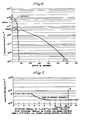
- Breakdown of the junction occurs at the intersection of the phosphorous and boron curves. For the left-hand phosphorous curve, this will be at BV(1). However, with a slight shift in phosphorous depth, represented by the right-hand curve, the intersection will be at BV(2), representing a signficantly higher breakdown voltage. Thus it will be seen that an unacceptably large variation in results can occur, as the depth of diffusion varies only slightly from unit to unit. In fact, if the breakdown voltage of the buried p/n junction becomes high enough, unstable surface-junction breakdowns will occur instead, i.e. if BVEBO ⁇ BVZ then the breakdown will occur at the surface, and will likely be unstable. Thus the characteristics presented by Figure 1 represent a serious difficulty with known procedures.
- a deep ion implantation 20 of p++ boron is first made into the epitaxial layer of the wafer. This implantation is made with a generally circular cross-section, of relatively small diameter.
- a shallower boron ion implantation, generally indicated at 22, is made to overlie the original deep implantation 20. This shallower implantation is of lower concentration (p+) and extends out laterally on opposite sides of the p++ implant, along a line BB', forming approximately rectangular regions 24, 26, identified as base regions.
- the shallow p+ implantation also includes a reduced-width central segment 28 joining the base regions 24, 26, and positioned symmetrically over the circular deep p++ implantation 20.
- the base regions 24, 26 and the joining segment 28 enable electrical connection to be made to the deep p++ ion implantation region 20.
- n++ arsenic ion implantation 30 then is made over the original p++ implantation 20 and portions of the central p+ segment 28. This implantation is arranged to extend laterally well beyond the edges of the p++ implantation and, as seen in Figures 2 and 3, forms a horizontal sub-surface junction area 32 with the p++ implantation to define the buried-Zener diode.
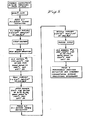
- the flow diagram of Figure 5 sets forth exemplary processing steps which can be used in forming the buried-Zener structure of Figures 2-4.
- the wafer is processed in accordance with standard preliminary procedures for bipolar ICs, as well known in the art.
- the wafer is provided with an oxide coating, e.g. 0,8 ⁇ m.
- Photo-resist then is applied, and a buried-Zener definition is effected (by a mask identified in the diagram as No. 2.7) to remove the oxide coating in the circular region 20 ( Figure 2). Thereafter, the wafer is subjected to ion implantation of boron, e.g. at an energy of between 20 and 200 keV and a concentration of 5-15 x 10 14 i o ns/cm 2 to form the p++ region 20.
- boron e.g. at an energy of between 20 and 200 keV and a concentration of 5-15 x 10 14 i o ns/cm 2 to form the p++ region 20.
- the hardened photo-resist over the remaining oxide on the wafer then is removed by a sulfuric acid strip (a procedure which does not affect the oxide coating). Thereafter a standard base masking step is carried out (Mask 3) with photo-resist, to define the base regions of the NPN transistors to be formed in the wafer. In this case, however, the base regions which are defined also include the two offset rectangular regions 24, 26 and the narrowed segment 28 over the p++ implantation 20.
- the first buried-Zener anneal then is carried out, e.g. at a temperature of 1150-1250°C for 30-300 minutes in a low oxygen ambient. This "drives in” the implanted boron to a substantial depth, desirably to about 3-6 microns, as illustrated in the sectional views of Figures 3 and 4. Also, the anneal serves to correct damage to the crystalline structure resulting from the ion implantation procedure.
- This anneal step includes a temperature ramp-down to 1000°C and a wet oxidation treatment to cover the bare silicon of the base regions with, for example, 0,2 - 0,6 ⁇ m of oxide.
- the field oxide will be augmented by this treatment, reaching a total thickness of perhaps 1 ⁇ m.
- a boron p+ implantation is carried out into the base regions 24, 26, 28 just defined.
- Such ion implantation may be carried out with an energy of 50-200 keV, and a concentration of 2-6 x 10 14 ions/cm 2 .
- the base implantation then is annealed at a temperature of ⁇ 1150°C for >30 minutes, in a low oxidating ambient, followed by a temperature ramp-down to 1000°C and a wet oxide treatment for about 20 minutes.
- Another photo-resist masking sequence then is carried out (Mask 3.5) to define the rectangular region 30 for the n++ arsenic ion implantation.
- This defined region is etched down to bare silicon, leaving the Base and field areas still covered by oxide.
- An n++ arsenic implantation then is made into the exposed area at an energy of 20-200 keV, and with a concentration of 2-10 x 10 15 ions/cm 2 .
- the remaining photo-resist layer in the non-defined regions helps to block implantation of arsenic ions in those areas.
- a plasma strip then is made, to take off the remaining (hardened) photo-resist material.
- This is followed by another buried-Zener anneal (#2), e.g. at a temper- atnre of 1000-1150°C for 10-90 minutes, together with a temperature ramp-down to 1000°C and wet oxidation for about 20 minutes.
- the offset regions 36, 38 joining the implanted n++ region 30 are defined by photo-resist.
- the standard emitter diffusion into the wafer produces corresponding diffusions in those regions 36, 38, as shown in the sectional views.
- these diffusions are made by chemical source diffusion for phosphorous in known fashion, although other techniques (doped oxide, ion implantation) might be used.
- surface contact metallization at the emitter regions 36, 38 establishes electrical connection to the n++ portion of the buried-Zener diode.
- surface contact metallization at the base regions 24, 26 establishes electrical connection to the p++ portion of the buried-Zener diode.
- Figure 6 is a graph showing the concentration' profile of a typical buried-Zener diode formed as described above. The boron and arsenic concentrations are shown as separate curves. A third curve represents the total concentration starting at the central point X on the wafer surface, as indicated in Figures 3 and 4. Figure 7 shows the variation in surface concentration of boron from point X to a laterally distant surface point X'.
- the position of the edge 30D (see Figure 2) of the n++ arsenic implant 30 is indicated in Figure 7 by the letter D. It will be seen from Figure 7 that the concentration of boron at this edge point (D) is about one-half to one-third of the concentration of boron at the sub-surface breadkown junction (see Figure 6). Thus, the Zener breakdown will take place predominantly at the sub-surface junction rather than at the surface, assuring stable diode operation at a desired voltage level.
- This specified ratio relationship between the boron concentrations at the surface and sub-surface junctions is moreover maintained consistently from unit to unit, at least in part due to the characteristics of ion implantation. Ion implantation is especially effective in that regard because superior control is exercised over the dopant concentration, i.e. the specified values can be held to much closer tolerances than heretofore. This is particularly true with respect to control of the surface breakdown characteristic.
- the use of arsenic to form the n++ region has been found to be quite advantageous, because the arsenic concentration profile is much more abrupt than that of phosphorous, and the implantation is shallower.
- the position of the p/n sub-surface junction is more controllably established, thereby reducing the degree of uncertainty in the concentration level of the boron at the junction, and requiring less boron.
- a modified Zener diode structure is shown in Figures 8-10.. This configuration provides for processing with only a single additional mask for forming the buried-Zener diode, rather than two additional masks as in the preferred embodiment described above.
- the wafer is first treated in accordance with the standard preliminary steps of bipolar processing, as well known in the art. Then, an oxide layer of > 0,4 ⁇ m formed on the wafer surface, and the conventional base region definition step is carried out (Mask 3).
- This definition step however includes formation of a Zener diode base region generally indicated at 50 (having essentially the same outline in plan view as the base 22 of Figure 2). This region is etched to bare silicon.
- the wafer receives a thin screen oxide layer of about 0,03 - 0,3/covering the bare silicon of the region 50.
- Nitride then is applied over the oxide to a depth of about 0,05 - 0,15 ⁇ m. It should be noted that any film which does not etch as rapidly as Si0 2 in HF may be used for this layer.
- the single additional mask (Mask 2.7) then is used to define an elongated rectangular area, generally indicated at 52, which will receive both an n++ and p++ ion implantation for the Zener diode.
- the region 52 In preparation for these implantations, the region 52 first is etched to remove the nitride, leaving the thin screen oxide in the generally square central section 54 of region 52.
- the rest of region 52 has the thicker oxide layer without any nitride covering.
- the rest of the base region 50, beyond the central section 54, has the thin oxide layer, covered by the nitride previously laid down, and hardened photo-resist.
- the remainder of the wafer, outside of regions 50 and 52, carries the thick oxide, covered by the nitride and hardened photo-resist.
- the p++ boron ion implantation now is made, illustratively at an energy of 50-200 keV and a concentration of 2-10 x 10 14 ions/cm 2 .
- An implantation of this intensity will pierce the thin oxide layer in the central section 54 and enter the silicon beneath that layer. In other areas, the ions will enter both the thick oxide layer and the hardened photo-resist over the nitride, but will not penetrate to the silicon in either case.
- the photo-resist then is stripped off by sulfuric acid, and a buried-Zener anneal is carried out, e.g. at 1150-1250°C for 30-300 minutes low oxygen ambient. This anneal drives in the p++ implant to a depth of about 3 - 6 microns, as generally illustrated at 56.
- the wafer is subjected to a buffered oxide etch, for about 10 minutes.
- This etch removes oxide at a rate of about 0,13 ⁇ m per minute, and thus in 10 minutes will strip the oxide from the elongate region 52, leaving bare silicon exposed.
- the etch does not strip off the nitride cover, there will be a lateral-etch removal of oxide beneath the nitride.
- This forms an under-cut region about the periphery of the elongate region 52, exposing bare silicon beyond the periphery of that region out to a distance of perhaps 2 microns or so.
- the nitride layer now is removed by a hot phosphoric etch, leaving the thin oxide coating over the base region 50 (except for the exposed silicon in the slightly enlarged central section 42), and also leaving the thick oxide layer in the field beyond the defined regions.
- a p+ implantation of boron ions now is made, for example, at an energy of 50-200 keV and a concentration of 2 - 6 x 10¹⁴ ions/cm2.
- This implantation enters the defined base region 50, including the bare silicon of the already- implanted central section 54 and the regions beyond the periphery of section 54. These latter regions carry the thin layer of oxide, but the ion implant energy is sufficient to pierce that oxide and penetrate the silicon. (It may be noted that the p+ implant also will enter the bare silicon of region 52 beyond central section 54, but this has no effect on the ultimate functioning of the device.
- a base anneal is carried out, for example at a temperature of ⁇ 1150°C for ⁇ 30 minutes in a low oxygen ambient.
- This anneal is followed by an arsenic n++ implant, illustratively at an energy of 30-200 keV, and a concentration of 2-10 x 10 15 ions/cm2.
- the arsenic ions will enter the bare silicon defined by the region 52, as enlarged by the under-cut region developed by the 10-minute buffered oxide etch carried out prior to removal of the nitride, as described above.
- Ions from this arsenic implantation will of course also enter the thin oxide layer in the base region 50 and the thick oxide layer elsewhere, but the thickness of the thin oxide and the energy of the implantation can be configured so that the arsenic ions have not sufficient range to penetrate to the silicon of the wafer.
- this incidental arsenic implantation is removed, to prevent diffusion of the ions into portions of the silicon where they could adversely affect performance.
- the wafer next is subjected to a 15-second buffered oxide etch, to remove about 0,1 ⁇ m of the oxide coatings. This eliminates the surface portions of the oxide carrying the arsenic ions.
- a low-temperature oxide (LTO) deposition is performed to build up a layer of about 0,6 ⁇ m on the bare silicon, as well as on the remaining oxide.
- LTO low-temperature oxide
- a second buried-Zener anneal now is performed, for example at a temperature of 1000-ll50°C for 10-90 minutes in a low oxygen ambient. This drives in the arsenic ions to form the final junction dispositions for the buried-Zener diode.
- a horizontal sub-surface junction 58 is formed between the n++'ions and the already implanted p++ ions.
- an offset emitter region 60 is defined for the buried-Zener diode.
- the conventional phosphorous diffusion into the wafer produces at this region 60 a corresponding diffusion which overlaps the arsenic ion implantation region (see Figure 10). Formation of surface contact metallization at this diffusion 60 establishes electrical connection to the n++ arsenic implant of the buried-Zener diode.
- the arsenic n++ diffusion into the bare silicon of region 52, as enlarged by the under-cut produced by the 10-minute buffered oxide etch, will overlap the original p++ boron implantation. That is, the n++ ions will extend out beyond the p++ ions in every direction. This lateral extension of the n++ ions in the base region 50 is sufficient so that the n++ ions will interface at the surface with the lower concentration (p+) boron ions of the base implantation, rather than the p++ ions.
- the surface junction between the arsenic and boron implants will occur in a region of lower boron concentration than exists at the horizontal sub-surface junction 58 between the arsenic n++ implant and the original p++ implant. Accordingly, the Zener breakdown will take place consistently at the sub- surface junction rather than at the surface junction,assuring stable diode operation at a desired voltage level.
- Equipment for performing such implantation typically utilizes the principles of mass spectroscopy for separation of the ions to be implanted, followed by post acceleration of the ions to the required energy levels.
- Suppliers of such equipment include Varian and Eaton/Nova.
Landscapes
- Bipolar Transistors (AREA)
- Electrodes Of Semiconductors (AREA)
- Bipolar Integrated Circuits (AREA)
- Semiconductor Integrated Circuits (AREA)
- Element Separation (AREA)
- Semiconductor Memories (AREA)
Applications Claiming Priority (2)
| Application Number | Priority Date | Filing Date | Title |
|---|---|---|---|
| US60846984A | 1984-05-09 | 1984-05-09 | |
| US608469 | 1984-05-09 |
Publications (3)
| Publication Number | Publication Date |
|---|---|
| EP0160919A2 true EP0160919A2 (de) | 1985-11-13 |
| EP0160919A3 EP0160919A3 (en) | 1986-06-04 |
| EP0160919B1 EP0160919B1 (de) | 1991-09-25 |
Family
ID=24436636
Family Applications (1)
| Application Number | Title | Priority Date | Filing Date |
|---|---|---|---|
| EP85105255A Expired - Lifetime EP0160919B1 (de) | 1984-05-09 | 1985-04-30 | Verfahren zum Herstellen einer IC-Scheibe mit vergrabener Zenerdiode |
Country Status (5)
| Country | Link |
|---|---|
| EP (1) | EP0160919B1 (de) |
| JP (1) | JP2652153B2 (de) |
| CA (1) | CA1223086A (de) |
| DE (1) | DE3584184D1 (de) |
| IE (1) | IE57275B1 (de) |
Cited By (3)
| Publication number | Priority date | Publication date | Assignee | Title |
|---|---|---|---|---|
| EP0598438A1 (de) * | 1992-11-17 | 1994-05-25 | Koninklijke Philips Electronics N.V. | Verfahren zur Diffundierung von einem Dotierstoff in einem Halbleiter |
| EP0676802A1 (de) * | 1994-03-31 | 1995-10-11 | STMicroelectronics S.r.l. | Verfahren zur Herstellung eines Halbleiterbauteils mit vergrabenem Übergang |
| US10041013B2 (en) | 2012-12-20 | 2018-08-07 | Shell Oil Company | Fischer-Tropsch derived fuel compositions |
Families Citing this family (1)
| Publication number | Priority date | Publication date | Assignee | Title |
|---|---|---|---|---|
| JPS63184359A (ja) * | 1987-01-27 | 1988-07-29 | Toshiba Corp | 半導体装置の入力保護回路 |
Family Cites Families (9)
| Publication number | Priority date | Publication date | Assignee | Title |
|---|---|---|---|---|
| JPS5085284A (de) * | 1973-11-29 | 1975-07-09 | ||
| US4136349A (en) * | 1977-05-27 | 1979-01-23 | Analog Devices, Inc. | Ic chip with buried zener diode |
| JPS6014353Y2 (ja) * | 1977-06-24 | 1985-05-08 | ヤンマー農機株式会社 | コンバインにおける穀稈搬送チエンの緊張支持装置 |
| JPS5541770A (en) * | 1978-09-19 | 1980-03-24 | Nec Corp | Zener diode |
| JPS5583271A (en) * | 1978-12-20 | 1980-06-23 | Toshiba Corp | Semiconductor device |
| JPS5737884A (en) * | 1980-08-19 | 1982-03-02 | Nec Corp | Semiconductor device |
| JPS57147285A (en) * | 1981-03-05 | 1982-09-11 | Mitsubishi Electric Corp | Zener diode |
| US4441114A (en) * | 1981-12-22 | 1984-04-03 | International Business Machines Corporation | CMOS Subsurface breakdown zener diode |
| DE3151437A1 (de) * | 1981-12-24 | 1983-07-07 | Deutsche Itt Industries Gmbh, 7800 Freiburg | "verfahren zum herstellen einer vergrabenen zenerdiode" |
-
1985
- 1985-04-30 DE DE8585105255T patent/DE3584184D1/de not_active Revoked
- 1985-04-30 EP EP85105255A patent/EP0160919B1/de not_active Expired - Lifetime
- 1985-05-07 CA CA000480978A patent/CA1223086A/en not_active Expired
- 1985-05-08 IE IE1144/85A patent/IE57275B1/en not_active IP Right Cessation
- 1985-05-09 JP JP60096851A patent/JP2652153B2/ja not_active Expired - Lifetime
Cited By (5)
| Publication number | Priority date | Publication date | Assignee | Title |
|---|---|---|---|---|
| EP0598438A1 (de) * | 1992-11-17 | 1994-05-25 | Koninklijke Philips Electronics N.V. | Verfahren zur Diffundierung von einem Dotierstoff in einem Halbleiter |
| US5418184A (en) * | 1992-11-17 | 1995-05-23 | U.S. Philips Corporation | Method of manufacturing a semiconductor device in which dopant atoms are provided in a semiconductor body |
| EP0676802A1 (de) * | 1994-03-31 | 1995-10-11 | STMicroelectronics S.r.l. | Verfahren zur Herstellung eines Halbleiterbauteils mit vergrabenem Übergang |
| US5605851A (en) * | 1994-03-31 | 1997-02-25 | Sgs-Thomson Microelectronics S.R.L. | Method of forming semiconductor device with a buried junction |
| US10041013B2 (en) | 2012-12-20 | 2018-08-07 | Shell Oil Company | Fischer-Tropsch derived fuel compositions |
Also Published As
| Publication number | Publication date |
|---|---|
| JPS60249375A (ja) | 1985-12-10 |
| CA1223086A (en) | 1987-06-16 |
| EP0160919B1 (de) | 1991-09-25 |
| IE851144L (en) | 1985-11-09 |
| EP0160919A3 (en) | 1986-06-04 |
| IE57275B1 (en) | 1992-07-01 |
| DE3584184D1 (de) | 1991-10-31 |
| JP2652153B2 (ja) | 1997-09-10 |
Similar Documents
| Publication | Publication Date | Title |
|---|---|---|
| EP0401716B1 (de) | Verfahren zur Herstellung von komplementären NPN/PNP hoher Spannung | |
| EP0134166B1 (de) | Plättchenherstellung mittels Implantation durch Schutzschichten | |
| CA1082373A (en) | Method of forming an integrated circuit region through the combination of ion implantation and diffusion steps | |
| US20040224472A1 (en) | High voltage MOS transistor with up-retro well | |
| EP0442296A2 (de) | Hochgeschwindigkeits-SOI-Bauelement und Herstellungsverfahren dafür | |
| EP0536869A2 (de) | Verfahren zur Herstellung vergrabener Schichten vom P-Typ für PNP-Bauelemente | |
| US4601760A (en) | Ion-implanted process for forming IC wafer with buried-reference diode and IC structure made with such process | |
| US4473941A (en) | Method of fabricating zener diodes | |
| US4771011A (en) | Ion-implanted process for forming IC wafer with buried-Zener diode and IC structure made with such process | |
| US4672403A (en) | Lateral subsurface zener diode | |
| EP0118511B1 (de) | Verfahren zum herstellen eines kontakts für integrierte schaltung | |
| EP0017377B1 (de) | Verfahren zur Herstellung isolierter bipolarer Transistoren | |
| GB1577405A (en) | High-frequency transistors | |
| EP0160919B1 (de) | Verfahren zum Herstellen einer IC-Scheibe mit vergrabener Zenerdiode | |
| US4435225A (en) | Method of forming self-aligned lateral bipolar transistor | |
| US4758537A (en) | Lateral subsurface zener diode making process | |
| US4512815A (en) | Simplified BIFET process | |
| EP0143670A2 (de) | Verfahren zum Herstellen einer Halbleiteranordnung | |
| US4445270A (en) | Low resistance contact for high density integrated circuit | |
| US5439842A (en) | Low temperature oxide layer over field implant mask | |
| US4001050A (en) | Method of fabricating an isolated p-n junction | |
| EP0065463B1 (de) | Selbstalignierter lateraler Transistor und Verfahren zu seiner Herstellung | |
| EP0589674A2 (de) | Niedrigtemperatur Oxidschicht, auf einer Feld-Implantierungsmaske abgeschieden | |
| GB2038088A (en) | Semiconductor structures | |
| US5179030A (en) | Method of fabricating a buried zener diode simultaneously with other semiconductor devices |
Legal Events
| Date | Code | Title | Description |
|---|---|---|---|
| PUAI | Public reference made under article 153(3) epc to a published international application that has entered the european phase |
Free format text: ORIGINAL CODE: 0009012 |
|
| AK | Designated contracting states |
Designated state(s): DE FR GB NL |
|
| PUAL | Search report despatched |
Free format text: ORIGINAL CODE: 0009013 |
|
| AK | Designated contracting states |
Kind code of ref document: A3 Designated state(s): DE FR GB NL |
|
| 17P | Request for examination filed |
Effective date: 19861203 |
|
| 17Q | First examination report despatched |
Effective date: 19880922 |
|
| GRAA | (expected) grant |
Free format text: ORIGINAL CODE: 0009210 |
|
| AK | Designated contracting states |
Kind code of ref document: B1 Designated state(s): DE FR GB |
|
| RBV | Designated contracting states (corrected) |
Designated state(s): DE FR GB |
|
| REF | Corresponds to: |
Ref document number: 3584184 Country of ref document: DE Date of ref document: 19911031 |
|
| ET | Fr: translation filed | ||
| PLBI | Opposition filed |
Free format text: ORIGINAL CODE: 0009260 |
|
| 26 | Opposition filed |
Opponent name: PHILIPS ELECTRONICS N.V. Effective date: 19920625 |
|
| PGFP | Annual fee paid to national office [announced via postgrant information from national office to epo] |
Ref country code: GB Payment date: 19970429 Year of fee payment: 13 |
|
| PGFP | Annual fee paid to national office [announced via postgrant information from national office to epo] |
Ref country code: FR Payment date: 19970430 Year of fee payment: 13 |
|
| PGFP | Annual fee paid to national office [announced via postgrant information from national office to epo] |
Ref country code: DE Payment date: 19970627 Year of fee payment: 13 |
|
| APAC | Appeal dossier modified |
Free format text: ORIGINAL CODE: EPIDOS NOAPO |
|
| RDAG | Patent revoked |
Free format text: ORIGINAL CODE: 0009271 |
|
| STAA | Information on the status of an ep patent application or granted ep patent |
Free format text: STATUS: PATENT REVOKED |
|
| 27W | Patent revoked |
Effective date: 19970813 |
|
| GBPR | Gb: patent revoked under art. 102 of the ep convention designating the uk as contracting state |
Free format text: 970813 |
|
| APAH | Appeal reference modified |
Free format text: ORIGINAL CODE: EPIDOSCREFNO |
|
| PLAB | Opposition data, opponent's data or that of the opponent's representative modified |
Free format text: ORIGINAL CODE: 0009299OPPO |
|
| PLAB | Opposition data, opponent's data or that of the opponent's representative modified |
Free format text: ORIGINAL CODE: 0009299OPPO |