EP0161885B1 - Verstärkerschaltung - Google Patents
Verstärkerschaltung Download PDFInfo
- Publication number
- EP0161885B1 EP0161885B1 EP85303172A EP85303172A EP0161885B1 EP 0161885 B1 EP0161885 B1 EP 0161885B1 EP 85303172 A EP85303172 A EP 85303172A EP 85303172 A EP85303172 A EP 85303172A EP 0161885 B1 EP0161885 B1 EP 0161885B1
- Authority
- EP
- European Patent Office
- Prior art keywords
- stage
- field
- amplifier
- impedance
- circuit
- Prior art date
- Legal status (The legal status is an assumption and is not a legal conclusion. Google has not performed a legal analysis and makes no representation as to the accuracy of the status listed.)
- Expired
Links
- 230000005669 field effect Effects 0.000 claims description 29
- 239000003990 capacitor Substances 0.000 claims description 26
- 238000010586 diagram Methods 0.000 description 3
- 230000000903 blocking effect Effects 0.000 description 2
Images

Classifications
-
- H—ELECTRICITY
- H03—ELECTRONIC CIRCUITRY
- H03F—AMPLIFIERS
- H03F3/00—Amplifiers with only discharge tubes or only semiconductor devices as amplifying elements
- H03F3/181—Low-frequency amplifiers, e.g. audio preamplifiers
- H03F3/183—Low-frequency amplifiers, e.g. audio preamplifiers with semiconductor devices only
- H03F3/185—Low-frequency amplifiers, e.g. audio preamplifiers with semiconductor devices only with field-effect devices
- H03F3/1855—Low-frequency amplifiers, e.g. audio preamplifiers with semiconductor devices only with field-effect devices with junction-FET devices
-
- H—ELECTRICITY
- H03—ELECTRONIC CIRCUITRY
- H03F—AMPLIFIERS
- H03F1/00—Details of amplifiers with only discharge tubes, only semiconductor devices or only unspecified devices as amplifying elements
- H03F1/34—Negative-feedback-circuit arrangements with or without positive feedback
- H03F1/342—Negative-feedback-circuit arrangements with or without positive feedback in field-effect transistor amplifiers
Definitions
- the present invention relates to a multistage amplifier circuit constituted by cascade-connecting at least two field effect transistors (FETs), and more particularly to a simplified feedback type amplifier circuit which can improve frequency characteristics in a low frequency range.
- FETs field effect transistors
- a two-stage amplifier circuit as an example of a conventional multistage amplifier circuit constituted with at least two FETs cascade-connected to each other will be described with reference to Fig. 1.
- This amplifier circuit comprises a first-stage FET 1, the next (second)-stage FET 2 cascade-connected to the FET 1, and an interstage capacitor 3 connected between a drain D1 of the FET 1 and a gate G2 of the FET 2.
- Both drains D1 and D2 of the FETs 1 and 2 are connected commonly to a drain bias power supply terminal 6 through load impedances 4 and 5, respectively.
- sources S1 and S2 are grounded and gates G1 and G2 are connected to a gate bias terminal 9 through gate bias power feed impedances 7 and 8, respectively.
- a first amplifier stage comprised of the FET 1 is provided between the drain D1 and the gate G1 with a series circuit comprising first-stage feedback netwrok 10 and a capacitor 11 for blocking a dc component of a feedback singal (which will be called a dc block capacitor 11 hereinafter).
- the second amplifier stage comprised of the FET 2 is provided between the drain D2 and the gate G2 with a series circuit comprising a second stage feedback network 12 and a capacitor 13 for blocking a dc component of a feedback signal (which will be called a dc block capacitor 13 hereinafter).
- the amplifier circuit further comprises an input terminal 14 which is connected to the gate G1 of the FET 1, and an output terminal 15 which is connected to the drain D2 of the FET 2.
- the amplifier circuit when an input signal is supplied to the gate G1 through the input terminal 14, the input signal is amplified by the FET 1.
- the amplified output from the drain D1 of the FET 1 is inputted to the gate G2 through the interstage capacitor 3 and then is amplified by the FET 2, thus producing an output signal on the output terminal 15 connected to the drain D2 of the FET 2.
- negative feedbacks are implemented to both the FETs 1 and 2 through the first-stage feedback network 10 and the dc block capacitor 11 and through the second-stage feedback network 12 and the dc block capacitor 13, respectively.
- the conventional multistage amplifier circuit configured as shown in Fig. 1 is provided with a feedback circuit per each amplifier stage, it requires dc block capacitors 11 and 13 in the respective feedback loops in addition to the interstage dc block capacitor 3.
- the total capacitance value of capacitors has a great influence on the IC size to such a degree that it determines the IC size. For this reason, it is strongly required that the capacitance value of capacitors in the IC is as small as possible. To satisfy this requirement, first is to take the measure for reducing the number of capacitors used and second is to take the measure for configuring the IC at a minimum capacitance value required.
- the present invention has been made so as to eliminate such drawbacks and meet the above requirements and has for its object to provide an amplifier circuit which can improve frequency characteristic in a low frequency range with a simplified circuit configuration.
- the impedance circuit means of the present invention may be configured as an impedance circuit of less capacitive nature.
- the impedance circuit may comprise a resistance element, an inductance element, or a network comprising resistance and inductance elements coupled thereto.
- the gate of the (i - 1)th stage field-effect transistor has the same potential as that of the i-th stage field-effect transistor.
- the drain of the i-th stage field-effect transistor has the same potential as that of the (i - 1)th stage field-effect transistor.
- gates of the n number of field-effect transistors may be commonly connected to a gate bias terminal through impedance elements, respectively, drains of the n number of field-effect transistors may be commonly connected to a drain bias power supply terminal through load impedance elements, respectively.
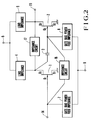
- Fig. 2 is a circuit diagram illustrating the embodiment of an amplifier circuit comprising a plurality of FETs successively connected to each other wherein by way of example, there is shown a two-stage amplifier circuit configured so that an input signal is applied to the gate of the first stage amplifier to produce an output signal from the drain of the next stage amplifier.
- the embodiment of the present invention is characterized in that there are provided a first impedance circuit means 16 for negative feedback which connects the gate G1 of the first-stage FET 1 to the gate G2 of the next-stage FET 2, and a second impedance circuit means 17 for negative feedback which connects the drain D1 of the first-stage FET 1 to the drain D2 of the next stage FET 2.
- first and second impedance circuit means provide impedance of feedback circuits provided in the first and second amplifier stages comprising FET 1 and the FET 2, respectively.
- Each impedance circuit means functions to allow a dc component of a feedback signal to pass therethrough. That is, this impedance circuit means is configured as an impedance circuit of less capacitive nature.
- the impedance circuit comprises a resistance element, an inductance element, or a network comprising resistance and inductance elements coupled to each other.
- An input signal from the input terminal 14 is applied to the gate G1 of the first-stage FET 1 and is amplified thereby.
- An output signal from the drain D1 of the first-stage FET 1 is inputted to the gate G2 of the next-stage FET 2 and is amplified thereby.
- an output signal is produced on the output terminal 15 connected to the drain D2 of the next-stage FET 2.
- the circuit component 16 functioning as impedance for negative feedback which provides a feedback impedance of the first-stage FET 1 between both gates G1 and G2 of the FET 1 and FET 2, at which potentials are equal to each other.
- the amplifier circuit when the amplifier circuit is caused to be operative under the condition where no current flows between the gate bias terminal 9 and each gate of the FETs, either of circuit elements 7 and 8 providing gate bias power feed impedance can be omitted.
- a potential at the drain D1 of the FET 1 can be equal to a potential at the drain D2 of the FET 2.
- a circuit component 17 functioning as impedance for negative feedback between the drains D1 and D2 of the FET 1 and the FET 2 and as a feedback circuit of the second-stage FET 2 it is possible to constitute a feedback type amplifier circuit without a dc block capacitor in the feedback loop.
- the present invention is applied to the two-stage amplifier circuit.
- the present invention is not limited to this embodiment. It is needless to say that the present invention is applicable to a multistage amplifier circuit comprising a plurality of FETs cascade-connected to each other.
- the number of dc block capacitors required therefor is (n - l).
- the improved amplifier circuit makes it possible to reduce the number of capacitors to less than one-half as compared to the (2n - l) capacitors required for the conventional amplifier circuit. Further, it is possible to omit each dc block capacitor provided in the feedback loop except for the dc block capacitor of the elementary feedback circuit in the first-amplifier stage. Thus, circuit configuration becomes simple, resulting in low cost and improvement in frequency characteristics in a low frequency range.
- the present invention can provide a simplified circuit configuration by improving the feedback system in a multistage type amplifier without using complicated means. Accordingly, this circuit is extremely advantageous in a practical use as follows: It is possible to reduce the required number of dc block capacitors to less than one-half when compared to the prior art circuit and to reduce the area of capacitors which is an important factor for determining the chip area when realizing an integrated circuit. Further, the feedback loop newly employed by the present invention is not provided with a dc block capacitor, thus enabling the improvement in frequency characteristics of the amplifier in a low frequency range. In addition, the amplifier circuit of the invention is quite effective in that the price can be reduced due to realization of simplified configuration.
Landscapes
- Engineering & Computer Science (AREA)
- Power Engineering (AREA)
- Multimedia (AREA)
- Amplifiers (AREA)
Claims (16)
- Verstärkerschaltung mit einer Anzahl n von Verstärkerstufen, die jeweils einen Feldeffekttransistor (1)(2) aufweisen, und miteinander über Zwischenstufenkondensatoren (3) miteinander kaskadenverbunden sind (wobei n eine ganze Zahl ist gleich oder größer 2), wobei ein Signal in die erste Stufe eingegeben und von der n-ten Stufe ausgegeben wird, dadurch gekennzeichnet, daßa) die (i -1)-te Verstärkerstufe (wobei i = 2, 3, 4 ... n ist) mit einer negativen Rückkopplungsschaltung (16) versehen ist, die eine Impedanzschaltungseinrichtung aufweist, die dazu dient eine DC-Komponente eines Rückkopplungssignals durchzulassen, wobei die in der (i - 1)-ten Verstärkerstufe vorgesehene Impedanzschaltungseinrichtung zwischen den zugehörigen Gates (G₁) (G₂) der Feldeffekttransistoren der (i - 1)-ten Stufe und i-ten Stufe verbunden ist, und daßb) die i-te Verstärkerstufe mit einer negativen Rückkopplungsschaltung (17) versehen ist mit einer Impedanzschaltungseinrichtung, die die gleiche Funktion wie die Impedanzschaltungseinrichtung der in der (i-1)-ten Verstärkerstufe vorgesehenen Rückkopplungsschaltung hat, wobei die in der i-ten Verstärkerstufe vorgesehene Impedanzschaltungseinrichtung zwischen zugehörigen Drains (D₁) (D₂) der i-ten und der (i-1)-ten Verstärkerstufen verbunden ist.
- Verstärkerschaltung nach Anspruch 1, dadurch gekennzeichnet, daß die Impedanzschaltungseinrichtungen (16) (17) jeweils als eine Impedanzschaltung mit niedriger Kapazität ausgeführt sind.
- Verstärkerschaltung nach Anspruch 1 oder Anspruch 2, dadurch gekennzeichnet, daß die Impedanzschaltungen (16) (17) jeweils ein Widerstandselement, ein Induktivitätselement oder ein Netzwerk aus miteinander verbundenen Widerstands- und Induktivitätselementen sind.
- Verstärkerschaltung nach einem der vorstehenden Ansprüche, dadurch gekennzeichnet, daß das Gate des Feldeffekttransistors der (i-1)-ten Stufe das gleiche Potential aufweist, wie das des Feldeffekttransistors der zweiten Stufe.
- Verstärkerschaltung nach einem der vorstehenden Ansprüche, dadurch gekennzeichnet, daß das Drain des Feldeffekttransistor der i-ten Stufe das gleiche Potential aufweist wie das des Feldeffekttransistors der (i - 1)ten Stufe.
- Verstärkerschaltung nach einem der vorstehenden Ansprüche, dadurch gekennzeichnet, daß die Gates der Anzahl n Feldeffekttransistoren jeweils über Impedanzelemente (7) (8) gemeinsam mit einem Gatevorspannungsanschluß (9) verbunden sind.
- Verstärkerschaltung nach Anspruch 6, dadurch gekennzeichnet, daS die Verstärkerschaltung unter der Bedingung betrieben werden kann, bei der die Anzahl der Impedanzelemente (7)(8) auf mindestens die Hälfte reduziert ist, wenn kein Strom zwischen jedem der Gates (G₁)(G₂) der Anzahl n Feldeffekttransistoren und dem Gatevorspannungsanschluß (9) fließt.
- Verstärkerschaltung nach einem der vorstehenden Ansprüche, dadurch gekennzeichnet, daß die Drains der Anzahl n Feldeffekttransistoren jeweils über Lastimpedanzelemente (4)(5) gemeinsam mit einem Drainvorspannung-Spannungsversorgungsanschluß (6) verbunden sind.
- Verstärkerschaltung nach einem der vorstehenden Ansprüche, dadurch gekennzeichnet, daß der Feldeffekttransistor (G₁) der ersten Stufe mit einem Eingangsanschluß (14) der mit dessen Gate verbunden ist, versehen ist, und daß der Feldeffekttransistor (G₂) der letzten Stufe mit einem Ausgangsanschluß (15), der mit dessen Drain (D₂) verbunden ist, versehen ist.
- Verstärkerschaltung von mindestens zwei Stufen von miteinander kaskadenverbundenen Feldeffekttransistoren (1)(2), einem Eingangsanschluß (14) für ein Eingangssignal, der in dem Feldeffekttransistor der ersten Stufe vorgesehen ist, einem Zwischenstufenkondensator (3), der zwischen aufeinanderfolgend verbundene Feldeffekttransistoren (1)(2) verbunden ist, und einem Ausgangsanschluß (15), der mit dem Drain (D₂) des Feldeffekttransistors der letzten Stufe verbunden ist, so daß ein verstärktes Signal von dem Ausgangsanschluß (15) ausgegeben wird, gekennzeichnet durch eine erste Impedanzschaltungseinrichtung (16) zum Bereitstellen einer negativen Rückkopplung, die es ermöglicht, daß eine DC-Komponente eines Rückkopplungssignals hindurchgelassen wird, wobei die erste Impedanzschaltungseinrichtung (16) zwischen zugehörigen Gates (G₁) (G₂) der Feldeffekttransistoren (1)(2) der ersten Stufe und der zweiten Stufe verbunden ist, eine zweite Impedanzschaltungseinrichtung (17) zum Bereitstellen einer negativen Rückkopplung, die die gleiche Funktion wie die erste Impedanzschaltungseinrichtung (16) hat, wobei die zweite Impedanzschaltungseinrichtung (17) zwischen den Drains (D₁) (D₂) des ersten und des zweiten Feldeffekttransistors (1)(2) verbunden ist.
- Verstärkerschaltung nach Anspruch 10, dadurch gekennzeichnet, daß die erste und die zweite Impedanzschaltungseinrichtung (16)(17) als eine Impedanzschaltung mit niedriger Kapazität ausgebildet ist.
- Verstärkerschaltung nach Anspruch 11, dadurch gekennzeichnet, daß eine Impedanzschaltung ein Widerstandselement, ein Induktivitätselement oder ein Netzwerk mit miteinander verbundenem Widerstand und Induktivität aufweist.
- Verstärkerschaltung nach Anspruch 10 oder Anspruch 11, dadurch gekennzeichnet, daß das Gate (G₁) des Feldeffekttransistors der ersten Stufe das gleiche Potential aufweist, wie das des Feldeffekttransistors der zweiten Stufe.
- Verstärkerschaltung nach Anspruch 10, wobei das Drain (D₁)(D₂) jeweils des ersten und des zweiten Feldeffekttransistors mit der zweiten Impedanzschaltungseinrichtung (17) verbunden ist, so daß das gleiche Potential vorhanden ist.
- Verstärkerschaltung nach Anspruch 10, dadurch gekennzeichnet, daß die Gates (G₁)(G₂) der Feldeffekttransistoren (1)(2), die miteinander in Kaskaden verbunden sind, jeweils über Impedanzelemente (7)(8) gemeinsam mit einem Gatevorsprungsanschluß (9) verbunden sind.
- Verstärkerschaltung nach Anspruch 10, dadurch gekennzeichnet, daß die Drains (D₁) (D₂) der Feldeffekttransistoren (1)(2), die miteinander in Kaskade verbunden sind, jeweils über Lastimpedanzelemente (4)(5) gemeinsam mit einem Drainvorspannungs-Spannungsversorgungsanschluß (6) verbunden sind.
Applications Claiming Priority (2)
| Application Number | Priority Date | Filing Date | Title |
|---|---|---|---|
| JP90225/84 | 1984-05-08 | ||
| JP59090225A JPS60235513A (ja) | 1984-05-08 | 1984-05-08 | 増幅回路 |
Publications (3)
| Publication Number | Publication Date |
|---|---|
| EP0161885A2 EP0161885A2 (de) | 1985-11-21 |
| EP0161885A3 EP0161885A3 (en) | 1988-01-20 |
| EP0161885B1 true EP0161885B1 (de) | 1992-01-02 |
Family
ID=13992539
Family Applications (1)
| Application Number | Title | Priority Date | Filing Date |
|---|---|---|---|
| EP85303172A Expired EP0161885B1 (de) | 1984-05-08 | 1985-05-03 | Verstärkerschaltung |
Country Status (6)
| Country | Link |
|---|---|
| US (1) | US4591802A (de) |
| EP (1) | EP0161885B1 (de) |
| JP (1) | JPS60235513A (de) |
| AU (1) | AU571816B2 (de) |
| CA (1) | CA1208315A (de) |
| DE (1) | DE3585050D1 (de) |
Families Citing this family (13)
| Publication number | Priority date | Publication date | Assignee | Title |
|---|---|---|---|---|
| DE3814041A1 (de) * | 1988-04-26 | 1989-11-09 | Standard Elektrik Lorenz Ag | Steuerbarer wechselspannungsverstaerker |
| FR2633119B1 (fr) * | 1988-06-21 | 1990-11-09 | Labo Electronique Physique | Circuit actif hyperfrequences du type passe-tout |
| FR2640444B1 (de) * | 1988-12-09 | 1991-03-15 | Labo Electronique Physique | |
| FR2644653B1 (fr) * | 1989-03-14 | 1991-05-31 | Labo Electronique Physique | Dispositif semiconducteur integre incluant un circuit isolateur actif |
| DE4240881C1 (de) * | 1992-12-04 | 1994-03-31 | Sel Alcatel Ag | Transistorverstärkerkaskade |
| JP2570961B2 (ja) * | 1993-04-14 | 1997-01-16 | 日本電気株式会社 | 半導体集積回路 |
| US5590412A (en) * | 1993-11-19 | 1996-12-31 | Sanyo Electric Co., Ltd. | Communication apparatus using common amplifier for transmission and reception |
| FR2763183A1 (fr) * | 1997-05-07 | 1998-11-13 | Philips Electronics Nv | Dispositif incluant un circuit amplificateur large-bande |
| US5977834A (en) * | 1998-04-03 | 1999-11-02 | Cbs Corporation | Preamplifier system |
| US6008694A (en) * | 1998-07-10 | 1999-12-28 | National Scientific Corp. | Distributed amplifier and method therefor |
| JP4652130B2 (ja) * | 2004-06-04 | 2011-03-16 | パナソニック株式会社 | 多段増幅装置、並びにそれを用いた受信回路及び送信回路 |
| US7128264B2 (en) * | 2004-07-23 | 2006-10-31 | Symbol Technologies, Inc: | Electro-optical reader with improved performance in high intensity ambient light |
| WO2008093477A1 (ja) * | 2007-01-30 | 2008-08-07 | Renesas Technology Corp. | Rf増幅装置 |
-
1984
- 1984-05-08 JP JP59090225A patent/JPS60235513A/ja active Granted
-
1985
- 1985-05-03 EP EP85303172A patent/EP0161885B1/de not_active Expired
- 1985-05-03 US US06/730,335 patent/US4591802A/en not_active Expired - Lifetime
- 1985-05-03 DE DE8585303172T patent/DE3585050D1/de not_active Expired - Lifetime
- 1985-05-06 CA CA000480791A patent/CA1208315A/en not_active Expired
- 1985-05-07 AU AU42032/85A patent/AU571816B2/en not_active Expired
Also Published As
| Publication number | Publication date |
|---|---|
| CA1208315A (en) | 1986-07-22 |
| EP0161885A2 (de) | 1985-11-21 |
| JPH0257722B2 (de) | 1990-12-05 |
| DE3585050D1 (de) | 1992-02-13 |
| EP0161885A3 (en) | 1988-01-20 |
| US4591802A (en) | 1986-05-27 |
| AU4203285A (en) | 1985-11-14 |
| AU571816B2 (en) | 1988-04-21 |
| JPS60235513A (ja) | 1985-11-22 |
Similar Documents
| Publication | Publication Date | Title |
|---|---|---|
| US4591802A (en) | Feedback amplifier circuit including cascade connected field effect transistors | |
| JP3811557B2 (ja) | 複数周波数帯域高効率線形電力増幅器 | |
| US6784749B1 (en) | Limiting amplifier with active inductor | |
| JPH01137710A (ja) | 広帯域増幅器 | |
| US20040169551A1 (en) | Active filter circuit with dynamically modifiable gain | |
| US5889426A (en) | Integrated circuit device having a bias circuit for an enhancement transistor circuit | |
| JPH06232657A (ja) | 高周波増幅器 | |
| US6496066B2 (en) | Fully differential operational amplifier of the folded cascode type | |
| US5367267A (en) | Broadband amplifier having individual input circuits with pluralities of capacitors and resistors | |
| JPH0758563A (ja) | ステップ減衰器 | |
| US4609889A (en) | Microwave frequency power combiner | |
| US5059922A (en) | High speed low offset CMOS amplifier with power supply noise isolation | |
| JP2682415B2 (ja) | 半導体集積回路 | |
| US7098743B2 (en) | Cascode amplifier | |
| US4943785A (en) | Controllable AC voltage amplifier | |
| JP2501311B2 (ja) | アクティブ・ロ−パス・フィルタ | |
| US5268650A (en) | Amplifier circuit with bipolar and field-effect transistors | |
| JP2594624B2 (ja) | 分布型増幅器 | |
| JPS63268303A (ja) | レベルシフト回路 | |
| JP3318149B2 (ja) | リミッタ増幅器 | |
| JPS59146229A (ja) | チユ−ナ装置 | |
| JPH0488708A (ja) | スイツチ回路 | |
| JPH06103808B2 (ja) | 分布型増幅器 | |
| JPH07112134B2 (ja) | 高周波増幅器 | |
| JPS63224508A (ja) | モノリシツクマイクロ波集積回路多段増幅器 |
Legal Events
| Date | Code | Title | Description |
|---|---|---|---|
| PUAI | Public reference made under article 153(3) epc to a published international application that has entered the european phase |
Free format text: ORIGINAL CODE: 0009012 |
|
| 17P | Request for examination filed |
Effective date: 19850510 |
|
| AK | Designated contracting states |
Designated state(s): DE FR GB NL |
|
| PUAL | Search report despatched |
Free format text: ORIGINAL CODE: 0009013 |
|
| AK | Designated contracting states |
Kind code of ref document: A3 Designated state(s): DE FR GB NL |
|
| 17Q | First examination report despatched |
Effective date: 19900312 |
|
| GRAA | (expected) grant |
Free format text: ORIGINAL CODE: 0009210 |
|
| AK | Designated contracting states |
Kind code of ref document: B1 Designated state(s): DE FR GB NL |
|
| REF | Corresponds to: |
Ref document number: 3585050 Country of ref document: DE Date of ref document: 19920213 |
|
| ET | Fr: translation filed | ||
| PLBE | No opposition filed within time limit |
Free format text: ORIGINAL CODE: 0009261 |
|
| STAA | Information on the status of an ep patent application or granted ep patent |
Free format text: STATUS: NO OPPOSITION FILED WITHIN TIME LIMIT |
|
| 26N | No opposition filed | ||
| PGFP | Annual fee paid to national office [announced via postgrant information from national office to epo] |
Ref country code: NL Payment date: 19970531 Year of fee payment: 13 |
|
| PG25 | Lapsed in a contracting state [announced via postgrant information from national office to epo] |
Ref country code: NL Free format text: LAPSE BECAUSE OF NON-PAYMENT OF DUE FEES Effective date: 19981201 |
|
| NLV4 | Nl: lapsed or anulled due to non-payment of the annual fee |
Effective date: 19981201 |
|
| PGFP | Annual fee paid to national office [announced via postgrant information from national office to epo] |
Ref country code: DE Payment date: 20000502 Year of fee payment: 16 |
|
| PGFP | Annual fee paid to national office [announced via postgrant information from national office to epo] |
Ref country code: GB Payment date: 20000503 Year of fee payment: 16 |
|
| PGFP | Annual fee paid to national office [announced via postgrant information from national office to epo] |
Ref country code: FR Payment date: 20000510 Year of fee payment: 16 |
|
| PG25 | Lapsed in a contracting state [announced via postgrant information from national office to epo] |
Ref country code: GB Free format text: LAPSE BECAUSE OF NON-PAYMENT OF DUE FEES Effective date: 20010503 |
|
| GBPC | Gb: european patent ceased through non-payment of renewal fee |
Effective date: 20010503 |
|
| PG25 | Lapsed in a contracting state [announced via postgrant information from national office to epo] |
Ref country code: FR Free format text: LAPSE BECAUSE OF NON-PAYMENT OF DUE FEES Effective date: 20020131 |
|
| PG25 | Lapsed in a contracting state [announced via postgrant information from national office to epo] |
Ref country code: DE Free format text: LAPSE BECAUSE OF NON-PAYMENT OF DUE FEES Effective date: 20020301 |