EP0161928A2 - Drehvorrichtung für ein tellerförmiges Übergabesystem - Google Patents
Drehvorrichtung für ein tellerförmiges Übergabesystem Download PDFInfo
- Publication number
- EP0161928A2 EP0161928A2 EP85303335A EP85303335A EP0161928A2 EP 0161928 A2 EP0161928 A2 EP 0161928A2 EP 85303335 A EP85303335 A EP 85303335A EP 85303335 A EP85303335 A EP 85303335A EP 0161928 A2 EP0161928 A2 EP 0161928A2
- Authority
- EP
- European Patent Office
- Prior art keywords
- transfer plate
- transfer
- pressure plate
- wafer
- chamber
- Prior art date
- Legal status (The legal status is an assumption and is not a legal conclusion. Google has not performed a legal analysis and makes no representation as to the accuracy of the status listed.)
- Granted
Links
Images




Classifications
-
- H—ELECTRICITY
- H10—SEMICONDUCTOR DEVICES; ELECTRIC SOLID-STATE DEVICES NOT OTHERWISE PROVIDED FOR
- H10P—GENERIC PROCESSES OR APPARATUS FOR THE MANUFACTURE OR TREATMENT OF DEVICES COVERED BY CLASS H10
- H10P72/00—Handling or holding of wafers, substrates or devices during manufacture or treatment thereof
- H10P72/30—Handling or holding of wafers, substrates or devices during manufacture or treatment thereof for conveying, e.g. between different workstations
- H10P72/33—Handling or holding of wafers, substrates or devices during manufacture or treatment thereof for conveying, e.g. between different workstations into and out of processing chamber
- H10P72/3308—Vertical transfer of a single workpiece
-
- C—CHEMISTRY; METALLURGY
- C23—COATING METALLIC MATERIAL; COATING MATERIAL WITH METALLIC MATERIAL; CHEMICAL SURFACE TREATMENT; DIFFUSION TREATMENT OF METALLIC MATERIAL; COATING BY VACUUM EVAPORATION, BY SPUTTERING, BY ION IMPLANTATION OR BY CHEMICAL VAPOUR DEPOSITION, IN GENERAL; INHIBITING CORROSION OF METALLIC MATERIAL OR INCRUSTATION IN GENERAL
- C23C—COATING METALLIC MATERIAL; COATING MATERIAL WITH METALLIC MATERIAL; SURFACE TREATMENT OF METALLIC MATERIAL BY DIFFUSION INTO THE SURFACE, BY CHEMICAL CONVERSION OR SUBSTITUTION; COATING BY VACUUM EVAPORATION, BY SPUTTERING, BY ION IMPLANTATION OR BY CHEMICAL VAPOUR DEPOSITION, IN GENERAL
- C23C14/00—Coating by vacuum evaporation, by sputtering or by ion implantation of the coating forming material
- C23C14/22—Coating by vacuum evaporation, by sputtering or by ion implantation of the coating forming material characterised by the process of coating
- C23C14/56—Apparatus specially adapted for continuous coating; Arrangements for maintaining the vacuum, e.g. vacuum locks
- C23C14/564—Means for minimising impurities in the coating chamber such as dust, moisture, residual gases
- C23C14/566—Means for minimising impurities in the coating chamber such as dust, moisture, residual gases using a load-lock chamber
-
- C—CHEMISTRY; METALLURGY
- C23—COATING METALLIC MATERIAL; COATING MATERIAL WITH METALLIC MATERIAL; CHEMICAL SURFACE TREATMENT; DIFFUSION TREATMENT OF METALLIC MATERIAL; COATING BY VACUUM EVAPORATION, BY SPUTTERING, BY ION IMPLANTATION OR BY CHEMICAL VAPOUR DEPOSITION, IN GENERAL; INHIBITING CORROSION OF METALLIC MATERIAL OR INCRUSTATION IN GENERAL
- C23C—COATING METALLIC MATERIAL; COATING MATERIAL WITH METALLIC MATERIAL; SURFACE TREATMENT OF METALLIC MATERIAL BY DIFFUSION INTO THE SURFACE, BY CHEMICAL CONVERSION OR SUBSTITUTION; COATING BY VACUUM EVAPORATION, BY SPUTTERING, BY ION IMPLANTATION OR BY CHEMICAL VAPOUR DEPOSITION, IN GENERAL
- C23C14/00—Coating by vacuum evaporation, by sputtering or by ion implantation of the coating forming material
- C23C14/22—Coating by vacuum evaporation, by sputtering or by ion implantation of the coating forming material characterised by the process of coating
- C23C14/56—Apparatus specially adapted for continuous coating; Arrangements for maintaining the vacuum, e.g. vacuum locks
- C23C14/568—Transferring the substrates through a series of coating stations
-
- Y—GENERAL TAGGING OF NEW TECHNOLOGICAL DEVELOPMENTS; GENERAL TAGGING OF CROSS-SECTIONAL TECHNOLOGIES SPANNING OVER SEVERAL SECTIONS OF THE IPC; TECHNICAL SUBJECTS COVERED BY FORMER USPC CROSS-REFERENCE ART COLLECTIONS [XRACs] AND DIGESTS
- Y10—TECHNICAL SUBJECTS COVERED BY FORMER USPC
- Y10S—TECHNICAL SUBJECTS COVERED BY FORMER USPC CROSS-REFERENCE ART COLLECTIONS [XRACs] AND DIGESTS
- Y10S414/00—Material or article handling
- Y10S414/135—Associated with semiconductor wafer handling
- Y10S414/139—Associated with semiconductor wafer handling including wafer charging or discharging means for vacuum chamber
Definitions
- the present invention relates to processing substrates in a vacuum chamber. More particularly, the field of the invention is sputter coating of semiconductor wafers, and apparatus for effecting such metallization coating of wafers individually, and on a serial, continuous basis.
- the invention is an improvement in the arrangement for rotating the transfer plate which carries the wafers from station to station within the sputtering apparatus.
- a wafer is introduced through the load lock and mounted in a transfer plate.
- the load lock is then pumped and the transfer plate is then rotated to move the wafer to a work station. While processing of the wafer is being conducted at the work station, a finished wafer is being unloaded at the load lock and a new wafer loaded.
- the pressure plate moves away from the transfer plate and the transfer plate moves away from the front wall.
- the transfer plate moves away from the front wall.
- the rotation is accomplished by a chain drive and hub system coupled to a motor.
- the chain drive is bulky and cumbersome.
- the rotational axis necessitates dynamic 0-ring seals which can cause vacuum leakage problems.
- the axial motion is mechanically independent, but synchronized by the controlling computer.
- the vacuum chamber of the wafer coating system is a large cylinder.
- the end walls are subject to considerable pressure which necessitates means for reinforcing the end walls.
- ribs were welded on these walls. The welding of the ribs causes problems of warping of the end walls.
- the object of the invention is to provide an improved transfer plate rotation system for use in coating systems which is rugged, compact, avoids dynamic 0-ring seals, provides greater precision of rotation angle, strengthens the vacuum chamber and integrates the rotational and axial motions.
- the coating apparatus includes internal wafer support means positioned within the chamber immediately inside of the entrance thereof, including means for releasably and resiliently gripping edgewise an individual wafer, to immediately accept a wafer upon insertion and permit instant release and removal upon completion of coating.
- the apparatus also includes load lock means including a movable closure member within the chamber to seal the wafer support means off from the remainder of the chamber interior and when the door of the entrance is opened, isolating the wafer and support means from the chamber environment during insertion and removal of a wafer.
- the support means includes an internal wafer transfer plate which rotates around a central axis in order to move wafers from the load lock to work stations within the coating apparatus and back to the load lock.
- a pressure plate aids in sealing the transfer plate to the front wall of the vacuum chamber.
- the system for rotating the transfer plate consists of a transfer plate driver assembly on the outside of the chamber at the axis and a transfer plate rotator assembly inside the chamber.
- the driver assembly consists of a pneumatic actuator for linear motion, a barrel cam which translates the linear motion into rotary motion with high torque at starting and stopping positions, and a rotary feedthrough all in a structural housing.
- the rotator assembly comprises a central hub with means for supporting the end walls, a transfer plate hub assembly and a ratchet arm connected to the rotary feedthrough. As the pressure plate assembly is drawn back by the ram, it in turn draws back the transfer plate and engages the ratchet arm with the transfer plate hub. The actuator then rotates the transfer plate. The ram then reverses direction, the ratchet arm disengages and is returned to its initial position.
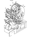
- the wafer coating system of FIG. 1 principally includes a generally cylindrical vacuum processing chamber 10 having five work stations, one of which comprises load lock arrangement 12, and one of which comprises coating station 14. Remaining further elements of the coating system found within chamber 10 may be seen in more detail in FIG. 2, which also shows a wafer 15 within load lock 12, and also a wafer at coating station 14. Further elements include pressure plate 16, wafer transfer plate assembly 18, and clip assemblies 20 (better shown in FIG. 3), by which a wafer is retained within wafer transfer plate assembly 18.
- These elements, together with cassette load/unload assembly 24 and the various ancillary vacuum pumps 25 for chamber and load lock evacuation, and control means, are all housed compactly in cabinet 26.
- the system desirably includes several other work stations other than load lock arrangement 12 and coating station 14, in particular wafer heating station 28, auxiliary station 29, and wafer cooling station 130. All five work stations are equally spaced laterally from each other and from the central axis 36 of the vacuum chamber. Also included are two pneumatic rams 30 and 31 which function to drive pressure plate 16 and wafer transfer plate assembly 18 against the front wall 32 of chamber 10, and transfer plate drive assembly 202 provides rotation of the transfer plate assembly about the central axis 36 of the vacuum processing chamber, as hereinafter described in detail in connection with FIGS. 8 and 9.
- wafers are individually presented and loaded by door assembly 22 into load lock arrangement 12 and thereby within wafer transfer plate 18.
- the wafer is then passed in turn to each of the work stations, where it is heated for completion of outgassing and/or sputter-etch cleaned, coated, optionally coated with a second layer, cooled, and then returned again to load lock 12 for removal from wafer transfer plate assembly 18, again by door assembly 22.
- the load lock arrangement 12 through which a wafer 15 must be passed in order to enter the evacuated environment of the chamber is of key importance.
- FIGS. 4-6 are especially important in appreciating the operation of the movable elements of load lock 12.
- the load lock is defined by a sandwich arrangement of elements between the chamber door assembly in its closed position against the front wall of the processing chamber and the pressure plate in its driven position.
- the load lock is built around a circular aperture 37 within wafer transfer plate assembly 18, which is positioned internally of the chamber just inside the chamber entrance 23 associated with load lock 12, with plate assembly 18 generally parallel to wall 32 and the pressure plate 16, positioned within the chamber rearwardly of plate assembly 18. Wafer 15 is loaded and held within the load lock and within the plate assembly by means which will be described below.
- the controlled subatmospheric environment which may be provided within chamber 10 for certain wafer processing operations may be, for example, up to 20 microns of argon or other inert gas for sputter coating operations. Because of this evacuated environment, the load lock region must be sealed off from the remainder of the chamber interior whenever door 22 is open in order to preserve the evacuated environment.
- Pressure plate 16 serves the function of isolating the load lock area from the chamber interior (and also several other functions simultaneously at other work stations, as will be shown below).
- Both pressure plate 16 and chamber front wall 32 are equipped with O-rings 38 arranged in a circular pattern concentric with chamber entrance 23 provide vacuum seals in the sandwich arrangement of elements defining the load lock.
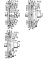
- FIGS. 4 and 6 show the completed load lock, with pressure plate 16 in its forward, advanced position, compressing plate assembly 18 against chamber wall 32, and sealing off aperture 37; and door 22 closed to seal off chamber entrance 23 to form the load lock about aperture 37, which is only of a size no larger than necessary to accommodate a single wafer.
- FIG. 5 shows pressure plate 16 in its withdrawn, rest position, and with the wafer already secured within plate assembly 18 within the chamber.
- wafer transfer plate assembly 18 which includes a plurality of circular apertures such as at 37 (as best seen in FIG. 2) matching the number and spacing of work stations within chamber 10.
- the apertures 37 are of a diameter larger than the wafers, are equally spaced from” each other, and centered at the same radial distance from the central axis of the processing chamber.
- the aforementioned work stations are likewise spaced, so that when any aperture of the wafer transfer plate assembly 18 is aligned with any work station of the processing chamber, the remaining apertures are each similarly aligned with a respective one of the remaining work stations.
- each of such wafers can be individually processed at a work station simultaneously with the processing of other wafers respectively at the remaining work stations.
- a wafer is individually processed at a given station, yet during the same time, several other wafers may also undergo other operations at the remaining work stations.
- another wafer may be coated at coating station 14, while still another wafer may be heated at heating station 28.
- the transfer plate driver assembly 202 intermittently operates to move plate assembly 18 by the distance of one station so as to serially present each of the wafers in turn to each of the processing stations in a counterclockwise direction, until a given wafer finally returns to the load lock for unloading therefrom.
- the details of the transfer plate rotation assembly 204 are not shown in FIG. 2 but are discussed hereinafter in connection with FIGS. 8 and 9.
- wafer carrier aperture 37 is of a diameter such that both a wafer and a set of clip assemblies 20 can be accommodated within the periphery of the aperture, and recessed and parallel with the transfer plate, thereby protecting the wafer.
- the set of thin edgewise-acting clip assemblies also is important to the formation of the thin load lock arrangement 12, and edgewise resiliently supports the wafer in an upright position within plate assembly 18. An especially advantageous form of such an edgewise acting clip assembly is shown in cross section in FIGS.
- a set of four clip assemblies 20 is mounted within retaining rings 41 which are removably attached to the disc-like circular wafer transfer plate 42 concentrically with each of plate apertures 37, thus forming the complete wafer transfer plate assembly 18.
- This arrangement mounts a set of clip assemblies 20 in spaced relationship within the periphery of each circular aperture 37.
- Retaining rings 41 are of U-shaped cross section, with each having flanges 46 and 47 defining the inner and outer peripheries thereof, and clip assemblies 20 are recessed within these flanges.
- clip assemblies 20 each include a block 50 of generally rectangular cross section, which may be of insulating material for applications such as sputter etch for which electrical isolation of the wafer is desired, and an elongated spring clip 53 firmly engaged in wraparound fashion about block 50.
- Each clip 53 includes at the end thereof opposite the block an arcuate finger portion or tip 55, which is of a curvature in radius appropriate to gripping an edge of a wafer.
- proximal flat portion 56 Extending from block 50 is proximal flat portion 56, which lies within a plane closely adjacent and parallel with the plane defined by plate aperture 37.
- distal portion 57 is angled away from portion 56 down toward the plane of plate aperture 37, and defines an obtuse angle with portion 56.
- This clip arrangement results in a plurality of arcuate tips 55 lying on a circular pattern of diameter somewhat less than that of a typical wafer 15 (such circular pattern also lies within the plane of wafer transfer plate 42).
- Wafer insertion into load lock 12 may be effected manually by simply pushing a wafer by its edge or rear face into clip assemblies 20. This will, however, involve some edge rubbing of the wafer against distal portion 56, to spread apart the clips somewhat to accept the wafer within tips 55. In order to insert a wafer without such rubbing contact therewith, the clips must first be slightly spread, and then allowed to rebound against the edge of the wafer upon insertion thereof into the load lock. Although both wafer insertion and clip spreading may be done manually, it is far preferable to avoid all such manual operations, and the consequent added risk of damage, error, and contamination associated therewith.
- Chamber door assembly 22 carries thereon a vacuum chuck 60 centrally axially therethrough, and a plurality of clip actuating means 62 near the periphery thereof. These elements, along with wafer cassette load/unload assembly 24, provide an automated wafer loading and unloading arrangement for load lock 12 which avoids all such manual handling of the wafers, and automates the loading process.
- chamber door assembly 22 is attached to front wall 32 of chamber 10 by a heavy-duty hinge 63 having a vertical axis, to allow the door to open and close in a conventional manner to a fully open position as shown, wherein the door and its inside face 64 are vertical and perpendicular to the plane of chamber entrance 23, as well as to plate assembly 18.
- Vacuum chuck 60 which extends axially and centrally through the door so that the active end thereof forms part of the inside face 64 of the door, engages a wafer presented vertically to the inside face of the door and holds the wafer by vacuum suction as the door is closed, whereupon the vacuum chuck axially extends from the inner door face as shown in FIG.
- the vacuum chuck will then withdraw, and wafer 15 is held in the chamber by the clip assemblies and undergoes processing, and movement to the various work stations in turn by rotation of plate assembly 18.
- the vertical presentation of the wafer to the inside face 64 of the door is effected by load/unload assembly 24, as will be further detailed below.
- the load lock arrangement, wafer transfer plate assembly 18, and door assembly 22 need not be limited to a vertical orientation, although this is preferred to help obviate any possibility of debris settling upon a surface of the wafer or sputter target.
- the clip assembly, transfer plate and load lock arrangement of the invention, as well as all of the work stations, function equally well if oriented horizontally.
- the load/unload assembly 24 for the vertically-oriented wafer cassettes is meant for vertical operation
- the door assembly 22 could easily be made to load wafers into the load lock in a horizontal plane, yet accept wafers in a vertical orientation, by suitable modification of its manner of mounting to the chamber wall in a conventional manner.
- each clip actuating means 62 is mounted so as to be in registration with a corresponding one of clip assemblies 20 when the door is in its closed position.
- Each clip actuating means 62 shown in detail in FIG.
- pins 66 are each in registration with one of flat proximal clip portions 56 when the door is in its closed position. With door 22 closed, pins 66 are extended just prior to insertion of a wafer, or as a wafer is to be withdrawn. The pressure of a pin 66 against the facing flat clip proximal portion 56 presses the clip and causes the tip 55 to swing back and outwardly, thereby releasing the clips, to facilitate insertion or removal of a wafer without rubbing contact therewith.
- cassette load/unload assembly 24 which includes wafer elevator assembly 68 and wafer cassette conveyor assembly 69.
- the conveyor assembly Extending below and on either side of chamber entrance 23 and attached to wall 32 of the chamber is the conveyor assembly, which moves cassettes 70 of wafers generally along from the right of the entrance as shown in FIG. 1 to left.
- the cooperating wafer elevator assembly 68 lifts wafers individually from the cassettes conveyed by conveyor assembly 69 to the operative end of vacuum chuck 60 within the inside face 64 of door assembly 22, or lowers such wafers from the door upon completion of processing.
- Conveyor assembly 69 includes a spaced pair of parallel rails 72 and 73 extending horizontally and longitudinally across the front of wafer processing chamber 10.
- the rails support and convey cassettes 70, and the spacing of rails 72 and 73 is such that the sidewalls of the cassettes straddle the rail and enable the cassettes to be slidably moved along the rails across the conveyor assembly.
- Motive power for the movement of the cassettes is provided by chain drive means 75 which includes various guides and gear arrangements causing a roller chain to be moved alongside rail 72.
- the chain is provided at regular intervals with guide pins 76, which engage a matching cutout on the bottom of cassette wall 77 adjacent rail 72.
- a stepper motor means 80 is provided as the driving power for the chain means 75, to provide precise control over the movement of the cassettes, so that any chosen individual wafer within a cassette may be positioned for interaction with the wafer elevator assembly 68.
- the cassettes 70 hold a plurality of the wafers 15 in spaced, facing, aligned and parallel relationship, and are open at the top as well as over a substantial portion of their bottom, to permit access from below and above the wafers. They must be loaded so that the front faces of the wafers, which contain the grooves, steps, and other features defining the microcircuit components, face away from the inside face 64 of the open door 22, and so that the rear faces of the wafers face toward the door assembly. This ensures that when the vacuum chuck 60 engages the wafer, no contact is made with the front face containing the delicate microcircuits, and that the wafer is properly positioned upon insertion into the load lock 12 so that it will be oriented properly with respect to processing equipment within the processing chamber 10.
- the wafer elevator assembly 68 is positioned below and just to the left side of chamber entrance 23 and includes an upper guide plate 82, a blade-like elevator member 83, and an actuating cylinder 84 connecting to the lower end of member 83.
- Elevator blade member 83 is guided for movement up and down in a vertical path intersecting at right angles conveyor 69 between rails a72 and 73 to inside face 64 of door 22.
- Guide slot 85 in guide plate 82 just below the inside face of the door in the open position provides the uppermost guide for blade 83, while a vertical guide member 86 extending below the conveyor toward the actuating cylinder also aids in retaining blade 83 on its vertical path.
- the width of blade 83 is less than that of the spacing between rails 72 and 73, and also less than the spacing between the main walls of the cassettes 70 which straddle rails 72 and 73. Blade 83 is also thinner than the spacing between adjacent wafers retained in cassettes 70.
- Blade member 83 is further provided with an arcuate upper end 87 shaped to match the curvature of the wafers, and a groove within this end adapted to match the thickness of a wafer and retain a wafer edgewise therewithin.
- elevator blade member 83 passes between guide rails 72 and 73 and intersects conveyor and cassette at right angles thereto, upon stepper motor means 80 and chain drive 75 bringing a cassette and wafer into registration over the path of the blade.
- the cassettes are constructed to allow access from below to the wafers, and to allow elevator blade 83 to pass completely therethrough.
- blade 83 moves upwardly between the conveyor rails to engage from below a wafer within the groove of its upper end 87, and elevate the wafer upwardly to a position in registration concentrically with and immediately adjacent inside face 64 of chamber door 22 in its open position. Note that since the wafers are vertically oriented, gravity aids in holding the wafers firmly yet gently and securely in the grooved end 87 of the blade.
- vacuum chuck 60 engages wafer 15 at its rear face by suction, and elevator blade 83 then is lowered through guide slot 85 and the cassette to a point below conveyor 69.
- Door 22 then closes with the wafer retained by the chuck 60, and the wafer is thereby loaded into the load lock arrangement 12 and chamber entrance 23 sealed simultaneously as described above for processing within chamber 10.
- still further wafers may be loaded within the remaining ones of apertures 37 of plate assembly 18; therefore the stepper motor and chain drive step the cassette one wafer position to move the next wafer serially in position over blade 83.
- Blade 83 then rises to repeat its operation of moving this next wafer upwardly to the open door, whose vacuum chuck then again engages that wafer for insertion into the load lock.
- vacuum chuck 60 again extends to the backside of the wafer while the door is still in its closed position, and clip actuating means 62 simultaneously depress the clips to disengage same from the wafer to enable the removal thereof by chuck 60, whereupon the door is opened and the wafer again positioned over the path of blade 83.
- stepper motor means 80 and chain means 75 move the cassette back so that the original position of wafer 15 is presented over the blade path.
- Blade 83 then rises through conveyor rails 72 and 73 and slot 85 upwardly to engage the lower edge of wafer 15, whereupon chuck 60 releases the wafer, and enables blade 83 to lower the wafer back into its original position within the cassette. The cassette is then propelled forward to the position of the next wafer to be processed serially.
- FIGS. 4 and 5 show in more detail the relative positioning of the pressure plate and wafer trasnfer plate, with FIG. 4 showing the aforementioned sandwich arrangement of the elements defining the load lock arrangement 12, and FIG. 5 showing the relative positioning of the elements when the pressure plate is in its withdrawn position.
- FIG. 4 shows vacuum chuck 60 in its extended position as the wafer is inserted into clip assemblies 20 with pins 67 of clip actuating means 62 partially extended after having spread the clips; while in FIG.
- the vacuum chuck has withdrawn, as have the pins of the clip actuating means, and the wafer is now securely mounted in wafer transfer plate assembly 18. With pressure plate 16 withdrawn, the wafer is now ready to be rotated to subsequent processing stations.
- the vacuum chuck is also in the withdrawn position; however, the vacuum suction is operative, and the wafer is shown in its position against the inner face 64 of chamber door 22. This is, of course, the position of the elements of the load lock and the wafer just after the wafer has been withdrawn from clip assemblies 20, prior to its being removed from the load lock; or, it also represents the position of the elements just after'-the door has been closed and the vacuum chuck has not yet advanced the wafer to its position within aperture 51 of the wafer carrier assembly. Pins 67 of the clip actuating means 62 are shown bearing upon the clips just prior to depressing same to spread the clips in order to accept the wafer therewithin.
- the load lock chamber Upon completion of loading of the load lock with a wafer 15, the load lock chamber is pumped down to a level compatable with the processing chamber environment before the pressure plate is withdrawn as shown in FIG. 5, and the wafer 15 rotated to the first work station.
- pressure plate 16 While a wafer is being loaded into and/or unloaded from load lock station 12, pressure plate 16 is in its active advanced position of FIG. 4, whereby plate assembly 18 is forced against front wall 32 of the chamber, the pressure plate is similarly urging wafers in the remaining stations into contact or closer, working cooperation with the processing devices at those stations; for example, the first or heating station 28.
- the next station (see FIGS. 1 and 9) to which the wafer is advanced is coating station 14, where a sputter coating source 100 is mounted on the back plate 99 of the chamber, and for which an aperture 101 of circular form is made within the pressure plate, to enable the sputtering source to direct coating therethrough to a wafer advanced by transfer plate assembly 18 into registration at the coating station.
- a shutter 102 is also provided to enable the coating material to be blocked during rotation of the transfer plate assembly and when a wafer is not present at the coating station.
- the next station to which the wafer 15 is advanced is a second coating station 128.
- station 130 which may be a cooling station.
- the final station to which wafer 15 is advanced is the load lock station 12, from which the wafer is removed and returned by means of load/unload assembly 24 to the same slot in the cassette 70 from which it originally came.
- the entire load/unload operation was described in detail earlier.
- the wafer 15 is presented vertically to the inside face of chamber door 22, where it is engaged by vacuum chuck 60.
- Vacuum chuck 60 and clip actuating means 62 are mounted within the chamber door 22.
- Chamber door 22 is the outer door of load lock arrangement 12.
- a further embodiment is one in which the wafer loading/unloading means retracts after loading the wafer into wafer transfer plate assembly 18, following which a separate O-ring-sealed door is brought into position to effect the outer seal for the load lock.
- the transfer plate rotation system is shown in FIGS. 8 and 9.
- the front wall plate 32 of the chamber separates the transfer plate driver assembly 202 from the transfer plate rotation assembly 204.
- a pneumatic or electromechanical activator 206 drives a barrel cam 210 axially along the direction of arrow line 205 by means of shaft 207.
- the barrel cam 210 is supported by'two cam rollers 208 in straight slots 220 formed into opposite sides of the barrel. Each cam roller 208 is mounted through a boss 256 and fastened with a nut 254.
- Cam rollers 222 riding in the sine slots 218 are attached to the center drive shaft 219 of a rotary feedthrough 212 such as those sold by the Ferrofluidic Corp.
- Axial movement of shaft 207 causes axial movement of cam 210 and thus rotational movement of feedthrough shaft 217.
- the sine slots 218 are cut in a sinusoidal shape so as to develop maximum torque at the beginning and end of each movement.
- the rotary feedthrough 212 is threaded into the front plate 32 and sealed with the 0-ring 258.
- the transfer plate driver assembly is in a structural housing 214.
- a first bushing 250 is made of a polyimide material such as "VESPEL®", sold by E. I. Dupont de Nemours and Company. First bushing 250 supports the shaft and ratchet arm 238 having ratchet tip 240.
- the transfer plate assembly 18 is attached to the transfer plate hub assembly 230.
- the pressure plate 16 is attached to the pressure plate hub assembly 228. Between the central hub 232 and the transfer plate hub assembly 230, there are second bushing 246 and third bushing 248. Between the transfer plate hub assembly 230 and the pressure plate hub assembly 228 there are fourth bushing 242 and fifth bushing 244. All bushings are made of the same material.
- a yoke 234 is bolted with spacing tubes 235 to the pressure plate hub assembly 228.
- the yolk 234 is fastened to the shaft 200 of a single pneumatic ram 31.
- Oversize holes are. formed in yoke 234 on its opposite edges to permit free passage two bolts 236 which are threaded into central hub 232.
- Bolts 236 are screwed outwardly to contact rear wall 99. In this way atmospheric pressure on the outside of the large flat walls 32 and 99 is prevented from bowing the walls inward when the inside of the chamber is under vacuum.
- a transfer plate index socket 252 of hardened steel is fastened to the end of the transfer plate hub assembly 230.
- the yolk 234 is drawn back which in turn draws back the pressure plate hub assembly 228 and the pressure plate 16.
- the fifth bushing 244 contacts the transfer plate index socket 252 which in turn draws back the transfer plate hub assembly 230 and the transfer plate 18.
- the transfer plate index socket 252 moves back one of five recesses 260 therein engages the ratchet tip 240.
- the transfer plate driver assembly 202 is used to apply torque via the actuator 206, the barrel cam 210, the rotary feedthrough 212, and the shaft 217 to the ratchet arm 238 which rotates by the appropriate angle.
- the appropriate angle would be 72 degrees.
- the ram shaft 200 is now forced toward the front of the chamber locking the pressure plate 16 and transfer plate assembly 18 in place to form the load lock seal as shown in FIGS. 4 and 6.
- the transfer plate driver assembly 202 is reversed, returning the ratchet arm 238 to its original position.
- the motion ratchet arm 238 is only back and forth through 72 degrees (for a five station system) so arm 238 does not contact bolts 236 or spacing collars 235.
- the motion of arm 238 is between the position of recesses 260a and 260b as shown in FIG. 9.
Landscapes
- Chemical & Material Sciences (AREA)
- Chemical Kinetics & Catalysis (AREA)
- Engineering & Computer Science (AREA)
- Materials Engineering (AREA)
- Mechanical Engineering (AREA)
- Metallurgy (AREA)
- Organic Chemistry (AREA)
- Physical Vapour Deposition (AREA)
- Testing Or Measuring Of Semiconductors Or The Like (AREA)
- Multi-Process Working Machines And Systems (AREA)
- Attitude Control For Articles On Conveyors (AREA)
- Container, Conveyance, Adherence, Positioning, Of Wafer (AREA)
Applications Claiming Priority (2)
| Application Number | Priority Date | Filing Date | Title |
|---|---|---|---|
| US611551 | 1984-05-17 | ||
| US06/611,551 US4548699A (en) | 1984-05-17 | 1984-05-17 | Transfer plate rotation system |
Related Child Applications (2)
| Application Number | Title | Priority Date | Filing Date |
|---|---|---|---|
| EP89114251.5 Division-Into | 1985-05-10 | ||
| EP89114251A Division EP0344823A3 (de) | 1984-05-17 | 1985-05-10 | Anlage zur Behandlung von Werkstücken |
Publications (3)
| Publication Number | Publication Date |
|---|---|
| EP0161928A2 true EP0161928A2 (de) | 1985-11-21 |
| EP0161928A3 EP0161928A3 (en) | 1987-10-28 |
| EP0161928B1 EP0161928B1 (de) | 1990-09-12 |
Family
ID=24449480
Family Applications (2)
| Application Number | Title | Priority Date | Filing Date |
|---|---|---|---|
| EP85303335A Expired EP0161928B1 (de) | 1984-05-17 | 1985-05-10 | Drehvorrichtung für ein tellerförmiges Übergabesystem |
| EP89114251A Withdrawn EP0344823A3 (de) | 1984-05-17 | 1985-05-10 | Anlage zur Behandlung von Werkstücken |
Family Applications After (1)
| Application Number | Title | Priority Date | Filing Date |
|---|---|---|---|
| EP89114251A Withdrawn EP0344823A3 (de) | 1984-05-17 | 1985-05-10 | Anlage zur Behandlung von Werkstücken |
Country Status (4)
| Country | Link |
|---|---|
| US (1) | US4548699A (de) |
| EP (2) | EP0161928B1 (de) |
| JP (1) | JPH0621357B2 (de) |
| DE (1) | DE3579622D1 (de) |
Cited By (3)
| Publication number | Priority date | Publication date | Assignee | Title |
|---|---|---|---|---|
| EP0448782A3 (en) * | 1990-03-26 | 1991-12-04 | Leybold Aktiengesellschaft | Apparatus for loading and unloading an article into a vacuum chamber |
| EP0389820B1 (de) * | 1989-03-30 | 1993-06-16 | Leybold Aktiengesellschaft | Vorrichtung zum Ein- und Ausschleusen eines Werkstücks in eine Vakuumkammer |
| EP0589416A1 (de) * | 1992-09-21 | 1994-03-30 | Nissin Electric Company, Limited | Schichtbildende Vorrichtung |
Families Citing this family (49)
| Publication number | Priority date | Publication date | Assignee | Title |
|---|---|---|---|---|
| DE3413001A1 (de) * | 1984-04-06 | 1985-10-17 | Leybold-Heraeus GmbH, 5000 Köln | Katodenzerstaeubungsanlage mit nebeneinander angeordneten stationen |
| JPS6169966A (ja) * | 1984-09-14 | 1986-04-10 | Hitachi Ltd | 真空処理装置 |
| US4790921A (en) * | 1984-10-12 | 1988-12-13 | Hewlett-Packard Company | Planetary substrate carrier method and apparatus |
| JPH07105345B2 (ja) * | 1985-08-08 | 1995-11-13 | 日電アネルバ株式会社 | 基体処理装置 |
| US4728863A (en) * | 1985-12-04 | 1988-03-01 | Wertheimer Michael R | Apparatus and method for plasma treatment of substrates |
| US4909695A (en) * | 1986-04-04 | 1990-03-20 | Materials Research Corporation | Method and apparatus for handling and processing wafer-like materials |
| CA1300357C (en) * | 1986-04-04 | 1992-05-12 | Materials Research Corporation | Method and apparatus for handling and processing wafer-like materials |
| US4915564A (en) * | 1986-04-04 | 1990-04-10 | Materials Research Corporation | Method and apparatus for handling and processing wafer-like materials |
| US5308431A (en) * | 1986-04-18 | 1994-05-03 | General Signal Corporation | System providing multiple processing of substrates |
| US4715921A (en) * | 1986-10-24 | 1987-12-29 | General Signal Corporation | Quad processor |
| US6103055A (en) * | 1986-04-18 | 2000-08-15 | Applied Materials, Inc. | System for processing substrates |
| US5102495A (en) * | 1986-04-18 | 1992-04-07 | General Signal Corporation | Method providing multiple-processing of substrates |
| CA1331163C (en) * | 1986-04-18 | 1994-08-02 | Applied Materials, Inc. | Multiple-processing and contamination-free plasma etching system |
| US5013385A (en) * | 1986-04-18 | 1991-05-07 | General Signal Corporation | Quad processor |
| US4670126A (en) * | 1986-04-28 | 1987-06-02 | Varian Associates, Inc. | Sputter module for modular wafer processing system |
| DE3716498C2 (de) * | 1987-05-16 | 1994-08-04 | Leybold Ag | Vorrichtung zum Ein- und Ausschleusen von Werkstücken in eine Beschichtungskammer |
| US4851101A (en) * | 1987-09-18 | 1989-07-25 | Varian Associates, Inc. | Sputter module for modular wafer processing machine |
| GB8729262D0 (en) * | 1987-12-15 | 1988-01-27 | Vg Instr Group | Sample treatment apparatus |
| US4795300A (en) * | 1988-01-20 | 1989-01-03 | The Perkin-Elmer Corporation | Loading apparatus for a work chamber |
| US5076205A (en) * | 1989-01-06 | 1991-12-31 | General Signal Corporation | Modular vapor processor system |
| US5259942A (en) * | 1989-03-30 | 1993-11-09 | Leybold Aktiengesellschaft | Device for transferring a workpiece into and out from a vacuum chamber |
| DE3912297C2 (de) * | 1989-04-14 | 1996-07-18 | Leybold Ag | Katodenzerstäubungsanlage |
| DE3912295C2 (de) * | 1989-04-14 | 1997-05-28 | Leybold Ag | Katodenzerstäubungsanlage |
| DE3943482C2 (de) * | 1989-05-08 | 1994-07-07 | Balzers Hochvakuum | Werkstückträger für ein scheibenförmiges Werkstück, sowie Vakuumprozeßkammer |
| IT1232241B (it) * | 1989-09-11 | 1992-01-28 | Cetev Cent Tecnolog Vuoto | Dispositivo per il caricamento veloce di substrati in impianti da vuoto |
| JPH07116586B2 (ja) * | 1990-05-31 | 1995-12-13 | 株式会社芝浦製作所 | バルブ機構を備えた配管装置 |
| JP3066507B2 (ja) * | 1990-11-30 | 2000-07-17 | 日本テキサス・インスツルメンツ株式会社 | 半導体処理装置 |
| DE4110490C2 (de) * | 1991-03-30 | 2002-02-28 | Unaxis Deutschland Holding | Kathodenzerstäubungsanlage |
| US5223112A (en) * | 1991-04-30 | 1993-06-29 | Applied Materials, Inc. | Removable shutter apparatus for a semiconductor process chamber |
| AU4652993A (en) | 1992-06-26 | 1994-01-24 | Materials Research Corporation | Transport system for wafer processing line |
| US5248371A (en) * | 1992-08-13 | 1993-09-28 | General Signal Corporation | Hollow-anode glow discharge apparatus |
| DE4302851A1 (de) * | 1993-02-02 | 1994-08-04 | Leybold Ag | Vorrichtung zum Anbringen und/oder Entfernen einer Maske an einem Substrat |
| GB9324002D0 (en) * | 1993-11-22 | 1994-01-12 | Electrotech Ltd | Processing system |
| US5753795A (en) * | 1996-05-10 | 1998-05-19 | Hewlett-Packard Company | Demountable vacuum-sealing plate assembly |
| JP3704883B2 (ja) * | 1997-05-01 | 2005-10-12 | コニカミノルタホールディングス株式会社 | 有機エレクトロルミネセンス素子及びその製造方法 |
| DE19742923A1 (de) | 1997-09-29 | 1999-04-01 | Leybold Systems Gmbh | Vorrichtung zum Beschichten eines im wesentlichen flachen, scheibenförmigen Substrats |
| US6328814B1 (en) | 1999-03-26 | 2001-12-11 | Applied Materials, Inc. | Apparatus for cleaning and drying substrates |
| US6413381B1 (en) | 2000-04-12 | 2002-07-02 | Steag Hamatech Ag | Horizontal sputtering system |
| US6264804B1 (en) | 2000-04-12 | 2001-07-24 | Ske Technology Corp. | System and method for handling and masking a substrate in a sputter deposition system |
| WO2003041131A2 (en) * | 2001-11-02 | 2003-05-15 | Applied Materials, Inc. | Single wafer dryer and drying methods |
| US7513062B2 (en) * | 2001-11-02 | 2009-04-07 | Applied Materials, Inc. | Single wafer dryer and drying methods |
| US7001491B2 (en) * | 2003-06-26 | 2006-02-21 | Tokyo Electron Limited | Vacuum-processing chamber-shield and multi-chamber pumping method |
| DE10355683B4 (de) * | 2003-11-28 | 2008-08-14 | Singulus Technologies Ag | Vakuumschleusenanordnung, Verfahren zum Transportieren eines Objekts mit der Vakuumschleusenanordnung und Verwendung der Vakuumschleusenanordnung zum Beschichten und Reinigen von Objekten |
| KR100614649B1 (ko) * | 2004-07-27 | 2006-08-23 | 삼성전자주식회사 | 웨이퍼 로딩 장치, 이를 이용한 반도체 제조 설비 및웨이퍼 로딩 방법 |
| JP5665679B2 (ja) * | 2011-07-14 | 2015-02-04 | 住友重機械工業株式会社 | 不純物導入層形成装置及び静電チャック保護方法 |
| RU2471883C1 (ru) * | 2011-11-23 | 2013-01-10 | Федеральное государственное унитарное предприятие "Научно-производственное предприятие "Исток" (ФГУП НПП "Исток") | Устройство для вакуумного нанесения материала |
| DE102016107990A1 (de) * | 2016-04-29 | 2017-11-02 | Von Ardenne Gmbh | Vakuumprozesskammer |
| CN111620086A (zh) * | 2020-05-20 | 2020-09-04 | 苏州悦力佳智能科技有限公司 | 一种应用于智慧工业的物料输送装置 |
| CN112366160B (zh) * | 2020-11-30 | 2021-08-20 | 杭州闻典通讯技术有限公司 | 一种计算机用节能型usb接口芯片自动生产设备 |
Family Cites Families (8)
| Publication number | Priority date | Publication date | Assignee | Title |
|---|---|---|---|---|
| FR1235463A (fr) * | 1959-05-27 | 1960-07-08 | Commissariat Energie Atomique | Perfectionnements aux dispositifs pour la production d'un mouvement de rotation discontinu |
| DE2034213C3 (de) * | 1969-10-10 | 1985-04-25 | Ferrofluidics Corp., Burlington, Mass. | Magnetdichtung zur Abdichtung von Dichtungsspalten |
| US3620584A (en) * | 1970-05-25 | 1971-11-16 | Ferrofluidics Corp | Magnetic fluid seals |
| US3796649A (en) * | 1971-12-13 | 1974-03-12 | Varian Associates | Coaxial sputtering apparatus |
| US4274936A (en) * | 1979-04-30 | 1981-06-23 | Advanced Coating Technology, Inc. | Vacuum deposition system and method |
| US4311427A (en) * | 1979-12-21 | 1982-01-19 | Varian Associates, Inc. | Wafer transfer system |
| US4756815A (en) * | 1979-12-21 | 1988-07-12 | Varian Associates, Inc. | Wafer coating system |
| US4416759A (en) * | 1981-11-27 | 1983-11-22 | Varian Associates, Inc. | Sputter system incorporating an improved blocking shield for contouring the thickness of sputter coated layers |
-
1984
- 1984-05-17 US US06/611,551 patent/US4548699A/en not_active Expired - Lifetime
-
1985
- 1985-05-09 JP JP60096853A patent/JPH0621357B2/ja not_active Expired - Lifetime
- 1985-05-10 EP EP85303335A patent/EP0161928B1/de not_active Expired
- 1985-05-10 EP EP89114251A patent/EP0344823A3/de not_active Withdrawn
- 1985-05-10 DE DE8585303335T patent/DE3579622D1/de not_active Expired - Lifetime
Cited By (5)
| Publication number | Priority date | Publication date | Assignee | Title |
|---|---|---|---|---|
| EP0389820B1 (de) * | 1989-03-30 | 1993-06-16 | Leybold Aktiengesellschaft | Vorrichtung zum Ein- und Ausschleusen eines Werkstücks in eine Vakuumkammer |
| EP0448782A3 (en) * | 1990-03-26 | 1991-12-04 | Leybold Aktiengesellschaft | Apparatus for loading and unloading an article into a vacuum chamber |
| EP0589416A1 (de) * | 1992-09-21 | 1994-03-30 | Nissin Electric Company, Limited | Schichtbildende Vorrichtung |
| US5482607A (en) * | 1992-09-21 | 1996-01-09 | Nissin Electric Co., Ltd. | Film forming apparatus |
| US5674368A (en) * | 1992-09-21 | 1997-10-07 | Nissin Electric Co., Ltd. | Film forming apparatus |
Also Published As
| Publication number | Publication date |
|---|---|
| EP0344823A2 (de) | 1989-12-06 |
| DE3579622D1 (de) | 1990-10-18 |
| JPS60244711A (ja) | 1985-12-04 |
| EP0161928B1 (de) | 1990-09-12 |
| EP0344823A3 (de) | 1990-01-03 |
| JPH0621357B2 (ja) | 1994-03-23 |
| EP0161928A3 (en) | 1987-10-28 |
| US4548699A (en) | 1985-10-22 |
Similar Documents
| Publication | Publication Date | Title |
|---|---|---|
| EP0161928B1 (de) | Drehvorrichtung für ein tellerförmiges Übergabesystem | |
| US4534314A (en) | Load lock pumping mechanism | |
| US4647266A (en) | Wafer coating system | |
| US4306731A (en) | Wafer support assembly | |
| US4311427A (en) | Wafer transfer system | |
| US4670126A (en) | Sputter module for modular wafer processing system | |
| US5096364A (en) | Wafer arm handler mechanism | |
| KR100483902B1 (ko) | 이온주입시스템용로드락어셈블리 | |
| JP3391623B2 (ja) | 半導体加工装置のためのローディング及びアンローディング用ステーション | |
| US8377210B2 (en) | Film forming apparatus | |
| US4717461A (en) | System and method for processing workpieces | |
| KR920005622B1 (ko) | 음극 스퍼터링 장치 | |
| JPS6379969A (ja) | ウェ−ハの貯蔵および移送方法および装置 | |
| US4779877A (en) | Wafer support assembly | |
| KR19990077004A (ko) | 이온주입 시스템용 이온빔 실드 | |
| EP1749116B1 (de) | Verfahren und vorrichtungen zur führung von gegenständen durch eine ladeschleusenkammer unter vakuum | |
| EP0244950B1 (de) | Verfahren und Vorrichtung zur Handhabung und Behandlung von scheibenartigen Materialien | |
| US5004924A (en) | Wafer transport apparatus for ion implantation apparatus | |
| US4873447A (en) | Wafer transport apparatus for ion implantation apparatus | |
| JP2884753B2 (ja) | イオン処理装置 | |
| JPH06132379A (ja) | 真空処理装置及び真空処理方法 | |
| JPH0367451A (ja) | イオン注入装置 | |
| JPS60214526A (ja) | 半導体製造装置 | |
| JPS635898B2 (de) | ||
| JPS6143158B2 (de) |
Legal Events
| Date | Code | Title | Description |
|---|---|---|---|
| PUAI | Public reference made under article 153(3) epc to a published international application that has entered the european phase |
Free format text: ORIGINAL CODE: 0009012 |
|
| AK | Designated contracting states |
Designated state(s): CH DE FR GB IT LI NL |
|
| 17P | Request for examination filed |
Effective date: 19860212 |
|
| PUAL | Search report despatched |
Free format text: ORIGINAL CODE: 0009013 |
|
| AK | Designated contracting states |
Kind code of ref document: A3 Designated state(s): CH DE FR GB IT LI NL |
|
| 17Q | First examination report despatched |
Effective date: 19890322 |
|
| GRAA | (expected) grant |
Free format text: ORIGINAL CODE: 0009210 |
|
| AK | Designated contracting states |
Kind code of ref document: B1 Designated state(s): CH DE FR GB IT LI NL |
|
| ITF | It: translation for a ep patent filed | ||
| ET | Fr: translation filed | ||
| REF | Corresponds to: |
Ref document number: 3579622 Country of ref document: DE Date of ref document: 19901018 |
|
| PGFP | Annual fee paid to national office [announced via postgrant information from national office to epo] |
Ref country code: GB Payment date: 19910501 Year of fee payment: 7 |
|
| PGFP | Annual fee paid to national office [announced via postgrant information from national office to epo] |
Ref country code: NL Payment date: 19910531 Year of fee payment: 7 Ref country code: DE Payment date: 19910531 Year of fee payment: 7 |
|
| PGFP | Annual fee paid to national office [announced via postgrant information from national office to epo] |
Ref country code: CH Payment date: 19910606 Year of fee payment: 7 |
|
| PLBE | No opposition filed within time limit |
Free format text: ORIGINAL CODE: 0009261 |
|
| STAA | Information on the status of an ep patent application or granted ep patent |
Free format text: STATUS: NO OPPOSITION FILED WITHIN TIME LIMIT |
|
| 26N | No opposition filed | ||
| PG25 | Lapsed in a contracting state [announced via postgrant information from national office to epo] |
Ref country code: GB Effective date: 19920510 |
|
| PG25 | Lapsed in a contracting state [announced via postgrant information from national office to epo] |
Ref country code: LI Effective date: 19920531 Ref country code: CH Effective date: 19920531 |
|
| PG25 | Lapsed in a contracting state [announced via postgrant information from national office to epo] |
Ref country code: NL Effective date: 19921201 |
|
| GBPC | Gb: european patent ceased through non-payment of renewal fee |
Effective date: 19920510 |
|
| NLV4 | Nl: lapsed or anulled due to non-payment of the annual fee | ||
| REG | Reference to a national code |
Ref country code: CH Ref legal event code: PL |
|
| PG25 | Lapsed in a contracting state [announced via postgrant information from national office to epo] |
Ref country code: DE Effective date: 19930202 |
|
| ITTA | It: last paid annual fee | ||
| PGFP | Annual fee paid to national office [announced via postgrant information from national office to epo] |
Ref country code: FR Payment date: 19940413 Year of fee payment: 10 |
|
| PG25 | Lapsed in a contracting state [announced via postgrant information from national office to epo] |
Ref country code: FR Effective date: 19960229 |
|
| REG | Reference to a national code |
Ref country code: FR Ref legal event code: ST |
|
| REG | Reference to a national code |
Ref country code: FR Ref legal event code: ST |