EP0163538B1 - Matériel pour la formation d'images, sa fabrication et son emploi - Google Patents
Matériel pour la formation d'images, sa fabrication et son emploi Download PDFInfo
- Publication number
- EP0163538B1 EP0163538B1 EP85303811A EP85303811A EP0163538B1 EP 0163538 B1 EP0163538 B1 EP 0163538B1 EP 85303811 A EP85303811 A EP 85303811A EP 85303811 A EP85303811 A EP 85303811A EP 0163538 B1 EP0163538 B1 EP 0163538B1
- Authority
- EP
- European Patent Office
- Prior art keywords
- resist
- resist material
- pattern
- coating
- layer
- Prior art date
- Legal status (The legal status is an assumption and is not a legal conclusion. Google has not performed a legal analysis and makes no representation as to the accuracy of the status listed.)
- Expired
Links
Images


Classifications
-
- G—PHYSICS
- G03—PHOTOGRAPHY; CINEMATOGRAPHY; ANALOGOUS TECHNIQUES USING WAVES OTHER THAN OPTICAL WAVES; ELECTROGRAPHY; HOLOGRAPHY
- G03F—PHOTOMECHANICAL PRODUCTION OF TEXTURED OR PATTERNED SURFACES, e.g. FOR PRINTING, FOR PROCESSING OF SEMICONDUCTOR DEVICES; MATERIALS THEREFOR; ORIGINALS THEREFOR; APPARATUS SPECIALLY ADAPTED THEREFOR
- G03F7/00—Photomechanical, e.g. photolithographic, production of textured or patterned surfaces, e.g. printing surfaces; Materials therefor, e.g. comprising photoresists; Apparatus specially adapted therefor
- G03F7/004—Photosensitive materials
- G03F7/075—Silicon-containing compounds
- G03F7/0757—Macromolecular compounds containing Si-O, Si-C or Si-N bonds
-
- Y—GENERAL TAGGING OF NEW TECHNOLOGICAL DEVELOPMENTS; GENERAL TAGGING OF CROSS-SECTIONAL TECHNOLOGIES SPANNING OVER SEVERAL SECTIONS OF THE IPC; TECHNICAL SUBJECTS COVERED BY FORMER USPC CROSS-REFERENCE ART COLLECTIONS [XRACs] AND DIGESTS
- Y10—TECHNICAL SUBJECTS COVERED BY FORMER USPC
- Y10S—TECHNICAL SUBJECTS COVERED BY FORMER USPC CROSS-REFERENCE ART COLLECTIONS [XRACs] AND DIGESTS
- Y10S438/00—Semiconductor device manufacturing: process
- Y10S438/942—Masking
- Y10S438/948—Radiation resist
Definitions
- the present invention relates to lithography, more particularly, to a pattern-forming resist or resist material suitable for forming a high quality resist pattern on a substrate or base material, usually a semiconductor, in the production of semiconductor integrated circuits and other semiconductor devices, for example, large-scale integrated circuits and bubble memory devices.
- the pattern-forming material is sensitive to high-energy radiation such as electron beams, X-rays, soft X-rays, and ion beams and is thermally stable.
- a plurality of pattern-forming resist materials is available for the purpose of recording the high-energy radiation described above.
- multi-layered resist coatings such as duplitized or two-layered resist coatings, and three-layered resist coatings.
- a multilayered resist coating is useful in the formation of fine patterns on uneven substrate using, for example, submicron electron beam lithography. This is because, as described hereinafter, the multi-layered resist coating effectively decreases scattering of electron beams and has an adverse influence on patterning, and/or a proximity effect. The differences in effect between a single resist layer and a duplitized resist coating in the electron beam lithographic process will be described with reference to Figs. 1 and 2.
- Figure 1 illustrates steps of a pattern formation process using a single resist layer.
- a substrate 1 has a single layer 2 of the resist material applied thereon.
- the resist layer 2 is irradiated with a pattern of electon beams (e-).
- the electron beams are undesirably scattered within the resist layer 2 (Scattering of electron means is shown by arrows a and b). Scattering a is caused due to the properties of the resist layer 2, while scattering b is caused by back scattering of the electron beams from the substrate 1.
- the illustrated scattering of the electron beams adversely affects the accuracy of the resulting resist pattern.
- the resulting resist pattern will show extension of the pattern ends.
- the width of the resist pattern will be increased due to back scattering of an electron beam on striking the substrate 1. In both of these cases, it is impossible or difficult to form fine resist patterns on the underlying substrate.
- the insufficient and undesirable patterning of the resist layer is apparent from Fig. 1(c), a cross-sectional view of the developed resist layer 12.
- Figure 2 shows a typical example of the use of the duplitized resist coating.
- the principle of the illustrated method is also applicable to the pattern-forming process of this invention.
- the substrate 1 has applied thereon a lower resist layer 3 and an upper resist layer 4 thinner than the layer 3.
- the thicker layer 3 is sandwiched between the substrate 1 and the thinner layer 4 and is formed from an organic resin having no sensitivity to the energy radiation used during the patterning of the layer 4.
- the layer 3 is also effective for levelling an uneven surface of the underlying substrate, for example, the surface of LSI chips, and therefore is generally referred to as a leveling layer.
- the exposed area of the upper resist layer 4 is insolubilized due to cross-linking of the resist material (see reference number 14 of Fig. 2(b)). Development is then carried out to remove the unexposed area of the resist layer 4.
- the patterned resist layer 14 is obtained.
- the pattern of the layer 14 is transferred to the underlying layer 3 by dry etching the layer 3 through the patterned layer 14, which acts as a mask or masking element.
- the patterned resist layer is shown in Fig. 2(c).
- the duplitized resist coating (3 plus 4) is free from scattering of the electron beams, since the upper layer 4 is very thin and the lower layer 3 is not effected by the electron beams during patterning of the upper layer 4. This effectively diminishes lateral extension of the pattern width. The effect is greater with lesser layer thicknesses of the layer 4. Further, increase of the layer thickness of the lower layer 3 diminishes the influence of back scattering of electron beams onto the patterning, thereby resulting in a decreased proximity effect. As a result, fine resist patterns with a high accuracy and a high aspect ratio can be obtained.
- the term "aspect ratio" used herein, as is generally recognized in the art, means the ratio of the layer thickness to the pattern width of the resist pattern. A high aspect ratio means that the resist pattern has a high accuracy of size.
- a prior art upper-layer forming resist material is chloromethylated polydiphenylsiloxane of the structural formula: which is referred to as SNR in this field.
- the resist material has a high resistance to oxygen plasma etching used in the etching of the underlying resist layer and shows an electron beam sensitivity of about 5 pC/cm 2 and a submicron resolution capability.
- P(SiSt-CMS) Another prior art upper layer-forming resist material, P(SiSt-CMS) reported in N. Suzuki et al: "Resist material for duplitized structure", 44th Symposium Preprint, 26a-U-7, Japan Society of Applied Physics, P.258, Sept. 1983.
- P(SiSt-CMS) namely, the copolymer of trimethyl- silylstyrene and chloromethyl styrene of the structure formula: is resistant to oxygen plasma and has an electron beam sensitivity of about 4 pC/cm 2 and a submicron resolution capability. Both of these resist materials, however, cause corrosion of the underlying aluminum or other metal circuit because they contain chlorine atoms.
- silicone resins having a ladder structure is highly sensitive to high-energy radiation such as electron beams or X-rays and is highly resistant to reactive ion etching, plasma etching spatter etching, or other dry etching and therefore is useful as a pattern-forming resist material (Japanese Unexamined Patent Publication (Kokai) No. 56 ⁇ 49540 and EP-A-00491 B).
- the resist material can be effectively used in the formation of the upper resist layer discussed above, but there are several difficulties when it is used in such a lithography process. First, the described resist material easily hardens when its coating is heated to evaporate the solvent therefrom.
- the hardened resist coating is insoluble in the developing solution and therefore cannot be used in the subsequent patterning steps. Heating of the coating resist material at a relatively low temperature is not desirable since it means a longer processing time. Second, the described resist material is thermally unstable and, therefore, cannot be stored for a long period without change of its properties. Third, it is impossible to prepare a monodispersed sample of the resist material which shows a high resolution capability. This is because the dependence of the solubility of the resist material or polysilsesquioxane on its hydroxyl equivalent and molecular weight makes the fractional precipitation process necessary for such preparation difficult.
- a high-energy radiation-sensitive pattern-forming resist material having improved sensitivity to electron beams, X-rays, proton beams and other high-energy radiation exposure, resistance to reactive ion etching, sputter etching, plasma etching, and other dry etching, improved resolution capability based on monodispersibility of the material or polymer, and thermal stability.
- the material should not cause corrosion of the underlying aluminum or other metal circuit if it is used in the production of semiconductor devices. Further, the material should be capable of being uniformly and thinly coated and should be effectively usable in the formation of a single resist layer as well as an upper layer of the duplitized resist coating.
- the coating comprises a substrate having coated thereon a leveling layer, a plasma etching-resistant layer, and a resist layer and therefore it necessitates lots of complicated and troublesome process steps.
- a pattern-forming resist material which consists of polysilsesquioxane having no hydroxyl group in its molecule has an improved sensitivity to high-energy radiation of up to an order of about 1 pC/cm 2 and a high resolution capability of about 0.3 to 0.5 pm I/s.
- the resist material is stable at a high temperature. It does not harden for about one hour at a temperature of less than 300°C, for example. Since the resist coating is not hardened during prebaking at about 100°C to 120°C, wherein the solvent is evaporated and adhesion to the underlying layer to be processed improved, the molecular weight of polysilsesquioxane and therefore the sensitivity and resolution capability of the resist coating can be maintained without deterioration.
- the resist material can be effectively used in the production of LSI's, very-large-small integrated circuits (VLSI's) and other semiconductor devices.
- the polysilsesquioxane of this invention suitable as the resist material, particularly negative-working resist material, is that represented by the formula: in which
- the polysilsesquioxane is trimethylsilylated polysilsesquioxane of the formula: in which R 1 , R 2 and m are defined above.
- a process for the production of a high-energy radiation-sensitive pattern-forming resist material which comprises condensing a trifunctional siloxane and removing active hydrogen atoms of the remaining unreacted hydroxy groups in the molecule, particularly its end portions and/or other portions, of the resulting condensate, by reacting the condensate with a monohalogenated silane as silylating agent thereby forming polysilsesquioxane having no hydroxyl group in its molecule.
- a useful silylating agent is monohalogenated silane of the formula: wherein groups R 4 may be the same or different and each represents hydrogen, a substituted or unsubstituted alkyl group or a substituted or unsubstituted aryl group, and X is a halogen, for example chlorine.
- Typical examples of the preferred silylating agents are (CH 3 ) 3 SiCl, (CICH 2 )(CH 3 ) 2 SiCl, (BrCH 2 )(CH 3 ) 2 SiCl, (C s H s )(CH 3 ) Z SICI, [(CH 3 ) 2 Si] 2 0 and NC(CH 2 ) 3 (CH 3 ) 2 SiCl.
- the silylating process is preferably carried out by using trimethylchlorosilane.
- the active hydrogen in the remaining hydroxyl group is reacted with the chlorine in the silane compound to form hydrogen chloride, which is then removed from the reaction system.
- a process for the formation of a resist pattern or an underlying substrate, such as semiconductor, or layer to be processed which comprises the steps of: coating on the substrate or layer a solution of a resist material according to the invention; drying the coated resist material in an inert gas; exposing the dried coating of the resist material to a desired pattern of high-energy radiation for patterning; and developing the patterned coating of the resist material.
- the resist material used in the pattern formation process of this invention is preferably a polysilsesquioxane represented by the formula (II) described above.
- the pattern formation process may further comprise dry etching the underlying substrate or layer through a mask, namely, pattern-wise developed coating of the resist material.
- the dry etching may be carried out by conventional means, such as plasma etching, a reactive ion etching, or sputter etching.
- another pattern formation process which comprises the steps of: coating on the substrate or layer a solution of a lower layer-forming first resist material which consists of an organic resin; drying the coated first resist material in an inert gas; further coating on the dried coating of the first resist material a solution of the upper layer-forming second resist material which consists of a polysilsesquioxane according to this invention; drying the overcoated second resist material in an inert gas; exposing the dried coating of the second resist material to a desired pattern of high-energy radiation for patterning; developing the patterned coating of the second resist material; and dry etching the underlying coating of the first resist material through a pattern-wise developed coating of the second resist material which acts as a mask, thereby transferring a pattern of the second resist coating to the underlying first resist coating.
- the organic resin suitable for the formation of the lower or first resist layer is preferably phenol resin, polyimide resin, or polystyrene resin. Epoxy resin, novolack resin, or related organic resins are also useful. Novolak resin or photoresist is commercially available, for example, from Shipley Co. under the tradename: MICROPOSIT AZ-1350.
- the organic resin is not limited to those resins, so long as it has no sensitivity to radiation used in the patterning of the upper resist layer, is not removed during development of the exposed upper resist layer, and has a high resistance to dry etching used to selectively etch the underlying substrate or layer. Of course, the organic resin should have no resistance to oxygen plasma etching, when such etching is used to transfer a pattern of the upper resist layer to the lower resist layer of the organic resin.
- the resist material suitable for the formation of the upper or second resist layer is preferably polysilsesquioxane of the above formula (I), more preferably, silylated polysilsesquioxane of the above formula (11) or (IIA).
- the upper resist layer is preferably thinner than the lower resist layer.
- the use of a thin layer is effective for obtaining a fine resist pattern having a high sensitivity and resolution capability.
- a satisfactorily high resistance to dry etching is also obtained.
- the lower resist layer is thick, it is possible to level the uneven features appearing on the surface of the substrate or layer to be selectively etched.
- the thickness of the upper resist layer is preferably about 0.2 to 0.5 11m and that of the lower resist layer preferably about 1.5 to 3.0 pm.
- the pattern formation process may further comprise dry etching the underlying substrate or layer through a pattern-wise etched coating of the first resist material which acts as a mask.
- the coating of the second resist material remaining on the first resist coating is generally removed during the dry etching step.
- a process for the production of semiconductor devices using a lithography technique which comprises dry etching the material to be etched through a mask formed from a high-energy radiation-sensitive pattern-forming resist material consisting of polysilsesquioxane having no hydroxyl group in its molecule, as discussed above.
- polysilsesquioxane can be easily produced by condensing trifunctional siloxanes.
- polymethylsilsesquioxane can be produced by the following reaction scheme: Namely, methyltrichlorosilane (IV) is first subjected to hydrolysis, and then the resulting hydrolysate (V) is condensed to form polymethylsilsesquioxane (VI).
- the finally resulting condensation product is not polymethylsilsesquioxane of the above formula (VI), but, in fact, polymethylsilsesquioxane having the following portions, for example: from which it is apparent that there are unreacted hydroxyl groups in the molecule of the condensation product.
- MIBK methyl isobutyl ketone
- TSA triethylamine
- Infrared (IR) spectrophotometric analysis of the resulting condensation product indicated that the product has the structure of formula (VII) described above. Further, gel permeation chromatography (GPC) using a column of polystyrene gel showed that the product (VII) had a molecular weight of about 20,000. The product, however, hardened after heating at about 80°C for 10 minutes, because of the presence of the unreacted hydroxyl groups.
- the polymethylsilsesquioxane used in this example starting to harden after heating at 60°C for 10 minutes.
- the resulting PMSS had a molecular weight of 4,000 and a degree of dispersion of 1.2. PMSS did not harden after heating at 150°C for 1 hour.
- mono-dispersed PMSS is effective to increase the resolution capability of the pattern-forming material. Such preparation is carried out by using a fractional precipitation process, which generally depends on two factors, namely, the hydroxyl equivalent and molecular weight of the polysilsesquioxane to be monodispersed. According to this invention, monodispersed PMSS having a degree of dispersion of less than 2.0 can be easily prepared, thereby resulting in fine resist patterns having a resolution capability of less than 0.5 pm I/s.
- PMSS of this invention has no hydroxyl groups and therefore the fractional precipitation process used in the preparation of monodispersed PMSS can be carried out on the sole basis of the differences of the molecular weight.
- the prior art polysilsesquioxane having hydroxyl groups is not suitable for the formation of monodispersed polysilsesquioxanes.
- PMSS (Molecular weight: 20,000; Degree of dispersion: 1.5) produced in Example 1 was dissolved in toluene.
- the toluene solution of PMSS as is shown in Fig. 3(a), was spin-coated on a silicon wafer or substrate 1 at a layer thickness of 0.5 pm.
- the PMSS resist layer 5 was then dried at 80°C for 15 minutes in a stream of nitrogen. After drying, the silicon wafer was conveyed into an electron beam exposure device (not shown) and was exposed to a pattern of electron beams at an accelation voltage of 20 kV. The irradiation of electron beams is shown with the reference symbol e- in Fig. 3(b).
- the irradiated area 15 of the resist layer was cross-linked and therefore insolubilized to a developer used in the subsequent development step.
- the silicon wafer was then dipped in a solution of methyl isobutyl ketone (MIBK) for one minute to develop the irradiated area 15 of the resist layer.
- MIBK methyl isobutyl ketone
- a fine resist pattern 15 having a resolution capability of 0.5 ⁇ m l/s was obtained (see Fig. 3(c)).
- the sensitivity was 7.0 x 10- 6 C/cm 2 .
- Example 3 The procedure of Example 3 was repeated, except that PMSS of Example 1 was replaced with PMSS (Molecular weight: 4,000; Degree of dispersion: 1.2) produced in Example 2 described above. A fine resist pattern having a resolution capability of 0.3 ⁇ m I/s was obtained. The sensitivity was 4.0 x 10- 5 C/cm 2 .
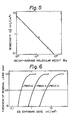
- FIG. 5 shows the relation between the weight-average molecular weight (Mw) of PMSS and its sensitivity (D g i ).
- PMSS-4 of this invention has a low (Mw) x (Dg l ) value.
- the value is lower in turn than that of PGMA, which is a prior art resist having a remarkably high sensitivity and the lowest among three silicone resists described in the table.
- the reason why PMSS having no functional group shows a remarkably high sensitivity is considered to be that it contains silicon atoms whose molecular weight is higher than that of the carbon atom, and the ratio of the silicon atoms contained in PMSS is higher than that of the other resist materials, and therefore shows notable internal scattering of electrons in the resist layer.
- Fig. 6 shows a sensitivity curve for each of PMSS-2, PMSS-3, and PMSS-4. From these graphs, it is clear that the higher the molecular weight of PMSS, the higher the sensitivity.
- PMSS of this invention exhibits a molecular weight and sensitivity of resolution capability of a relation similar to that of the prior art negative-working resist.
- the sensitivity is increased, but the resolution capability is decreased.
- the sensitivity and the resolution capability are in an inverse relation.
- PMSS is compared with that of the prior art resist, its decrease with the increase of the molecular weight is less than that of the prior art, since PMSS is a rigid high polymer having a ladder structure and no or little interlock of the molecular chains and therefore is rapidly soluble in a solvent.
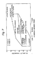
- Figure 7 is a graph of the range of good solvents for PMSS-2 and PMSS-4 of this invention.
- the graph indicates that the solubility of PMSS in a solvent varies remarkably depending upon its molecular weight.
- the polymeric compounds when their molecular weight is increased, tend to show a decreased solubility due to limitation of their movement in the solution. PMSS of this invention has this tendency, too.
- the tendency of PMSS is ramarkably greater than that of the polymeric compounds described above.
- PMSS of this invention is a high sensitivity resist material.
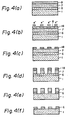
- Figures 4(a) through 4(f) are referred to.
- the silicon wafer was pattern-wise irradiated with an electron beam e- at an accelerating voltage of 20 KV.
- the irradiated area 18 of the upper PMSS layer was insolubilized.
- the silicon wafer was developed by dipping it in methyl isobutyl ketone (MIBK) for 30 seconds. The nonirradiated area of the upper PMSS layer was therefore removed. Subsequent to the development, the silicon wafer was rinsed in isopropyl alcohol (IPA) for 30 seconds and then postbacked at 80°C for 15 minutes in a gas stream of nitrogen. The result is illustrated in Fig. 4(c).
- MIBK methyl isobutyl ketone
- the silicon wafer was conveyed into a dry etching device of a parallel plate-shaped electrode type and dry etched with oxygen plasma (Gas pressure: 2PA; Applied power density: 0.22 W/cm 2 ) for 5 minutes.
- a dry etching device of a parallel plate-shaped electrode type and dry etched with oxygen plasma (Gas pressure: 2PA; Applied power density: 0.22 W/cm 2 ) for 5 minutes.
- the pattern of the upper PMSS layer 18 was transferred to the underlying photoresist layer 7.
- the upper PMSS layer 18 acted as an intermediate mask in the dry etching step.
- the tantalum coating 6 was etched with the plasma of the mixed gas CCl 4 /CF4(2:1) using a mask of the lower photoresist layer 7.
- the gas pressure was 8 Pa
- the applied power density was 0.33 W/cm 2
- the etching time was 4 minutes.
- the upper PMSS layer 18 was removed during the dry etching step.
- the remaining mask 7 of the photoresist was removed using a conventional removal technique.
- the silicon wafer having the patterned tantalum coating 6 was obtained.
- the resultion capability of the tantalum pattern was 0.25 11m I/S.
- the sensitivity was 10 ⁇ C/cm 2 .
- the resulting pattern of tantalum on the silicon wafer is unexpectedly effective as a mask for X-ray exposure, since X-rays do not permeate the tantalum patterns.
- tantalum atomic number 73, and atomic weight 181
- tantalum shows a large electron scattering characteristic or power, and therefore results in unacceptably large back scattering of the electron beam within the single resist layer.
- tantalum for X-ray exposure could not be produced.
- the resulting resist patterns had unacceptable bridges extending over the adjacent patterns.
- the tantalum patterns had a resolution capability of more than 1.5 Ilm I/s.
- This example is included to explain resist characteristics obtained when PMSS of this invention having a high glass transition temperature (Tg) is used as an upper layer-forming resist material in the duplitized resist process.
- Tg glass transition temperature
- Novolak photoresist Microposit 1350 commercially available from Shipley Co. was coated on a silicon wafer with a spin-coater and then baked at 200°C for one hour in a stream of nitrogen. A lower resist layer having a thickness of 1.5 11m was formed. Next, 0.4 g of PMSS was dissolved in 1.5 ml of toluene. The resulting upper layer-forming resist solution was spin-coated on the previously formed lower resist layer and baked at 80°C for 10 minutes in a stream of nitrogen. The dry thickness of the upper resist layer was 0.5 11m.
- the silicon wafer with the duplitized resist coating described above was pattern-wise exposed to an electron beam using an acceleration voltage of 20 KV.
- the exposure dose was controlled by varying the exposure time at a constant beam current.
- the upper resist layer was developed by dipping the wafer in a mixed solution of xylene and p-dichlorobenzene (3: 1) at a temperature of 23°C for 90 to 120 seconds. Thereafter, the lower resist layer was dry etched with oxygen plasma using a mask of the patterned upper resist layer.
- the applied power density was 0.33 W/cm 2 , gas pressure was 8 Pa, and etching time was 10 minutes.
- the pattern of the upper resist layer was transferred exactly to the underlying lower resist layer.
- PMSS and Microposit 1350 were tested as to the thickness of the residual layer as a function of the etching time. The results are plotted in Fig. 8.
- Figure 8 indicates that a PMSS resist layer does not cause a drop in layer thickness within the first 10 minutes of oxygen plasma etching, namely, it has a high resistance to oxygen plasma.
- the Microposit 1350 resist layer 1.5 pm thickness was gradually etched with time and was completely removed in about 6 to 7 minutes.
- 0.5% by weight of benzimidazole was added as a hardening accelerator to a mixture having a functional group equivalent ratio of 1:1.
- the resulting mixture was dissolved in cyclohexane to prepare a leveling solution.
- the leveling solution was spin-coated on a silicon substrate and baked at 200°C for 30 minutes in a gas stream of nitrogen. A leveling layer having a layer thickness of 2.0 pm was formed. Thereafter, a solution of PMSS resist was spin-coated on the leveling layer and baked at 80°C for 20 minutes in a stream of nitrogen. A 0.2 ⁇ m thick upper resist layer was formed.
- the silicon wafer with the duplitized resist coating described above was pattern-wise exposed to an electron beam using an acceleration voltage of 20 KV.
- the EB exposure dose was controlled by varying the exposue time at a constant beam current.
- the upper resist layer was developed by dipping the wafer in 4-methyl-2-pentanone for 60 seconds and then, in order to remove the developer, rinsing the wafer by dipping it in a mixed solution of acetone and isopropyl alcohol (IPA) (1:1) for 30 seconds.
- IPA isopropyl alcohol
- the underlying lower resist or leveling layer was dry etched with oxygen plasma using a mask of the patterned upper resist layer. The etching served to transfer a pattern of the upper resist layer to the leveling layer.
- the etch rate was determined after the 2 pm thick leveling layer was etched for a predetermined period. Further, the depth of the undercut or lateral etch was determined using a scanning electron microscope (SEM), after completion of the dry etching of the leveling layer with oxygen plasma using a mask of the patterned upper resist layer.
- SEM scanning electron microscope
- Fig. 9 indicates that the etch rate is increased with the increase of the applied power density, and that a peak for the etch rate is attained when the oxygen gas pressure is from 10 to 13 Pa. It is believed that a peak forthe etch rate curve occurs due to an increase or decrease of the oxygen gas pressure. The higher the gas pressure, the smaller the bestowed energy to the individual oxygen radical. At the same time, however the lower will be the total number of oxygen radicals.
- the leveling layer was dry etched using different oxygen gas pressures. Two power densities of 0.22 and 0.33 W/cm 2 were applied in the dry etching process. The results are plotted in Fig. 10.
- Figure 10 showing the variation of the'depth of the undercut as a function of the oxygen gas pressure, indicates that the lower the oxygen gas pressure or the higher the applied power density, the smaller the depth of the undercut. For example, when a power density of 0.22 W/cm 2 is applied, pattern transfer at an oxygen gas pressure of 2.0 Pa results in a small undercut of 0.07 pm. The depth of the undercut is increased with the increase of the gas pressure.
- the depth, at a gas pressure of about 10 to 13 Pa, at which pressure the etch rate of the leveling layer shows the highest value, is about 0.25 pm. It is, therefore, considered that, when the depth of the undercut is to be reduced to attain a high dimensional accuracy, the etching of the leveling layer must be carried out at a reduced gas pressure and at the same time the etch rate must be lowered. Further, when the applied power density is increased to attain a higher etch rate, much resist residue is formed on the substrate.
- the transfer time of the upper resist pattern to the leveling layer is shortened to about 16 minutes and the depth of the undercut is diminished to about 0.07 pm.
- the duplitized resist coating comprising an upper PMSS ⁇ 4 layer (0.2 pm thick) and a lower leveling layer (2.0 ⁇ m thick) was prepared, and tested as to its sensitivity characteristics.
- the results are plotted in Fig. 11.
- Figure 11 indicates that PMSS-4, when it is used as an upper layer of the duplitized resist coating, shows a remarkably improved sensitivity of 0.8 ⁇ C/cm 2 .
- the exposed upper PMSS-4 layer was developed with 4-methyl-2-pentanone and then rinsed with a mixed solution of acetone and isopropyl alcohol (IPA) (1:1). Thereafter, the lower leveling layer was dry etched with plasma oxygen at an oxygen gas pressure of 2.0 Pa and applied power density of 0.22 W/cm 2 .
- IPA isopropyl alcohol
- the silicon substrate a resist pattern of 0.5/0.7 pm I/s was formed on the substrate. Further, for the aluminium substrate, a resist pattern of 2.0/0.5 ⁇ m was formed. Furthermore, these submicron patterns showed a high aspect ratio of 4.4.
Landscapes
- Physics & Mathematics (AREA)
- General Physics & Mathematics (AREA)
- Spectroscopy & Molecular Physics (AREA)
- Photosensitive Polymer And Photoresist Processing (AREA)
- Exposure And Positioning Against Photoresist Photosensitive Materials (AREA)
- Materials For Photolithography (AREA)
Claims (14)


Applications Claiming Priority (4)
| Application Number | Priority Date | Filing Date | Title |
|---|---|---|---|
| JP59108521A JPS60254036A (ja) | 1984-05-30 | 1984-05-30 | パタ−ン形成方法 |
| JP108521/84 | 1984-05-30 | ||
| JP109503/84 | 1984-05-31 | ||
| JP59109503A JPS60254132A (ja) | 1984-05-31 | 1984-05-31 | パタ−ン形成材料 |
Publications (3)
| Publication Number | Publication Date |
|---|---|
| EP0163538A2 EP0163538A2 (fr) | 1985-12-04 |
| EP0163538A3 EP0163538A3 (en) | 1986-09-03 |
| EP0163538B1 true EP0163538B1 (fr) | 1989-11-23 |
Family
ID=26448377
Family Applications (1)
| Application Number | Title | Priority Date | Filing Date |
|---|---|---|---|
| EP85303811A Expired EP0163538B1 (fr) | 1984-05-30 | 1985-05-30 | Matériel pour la formation d'images, sa fabrication et son emploi |
Country Status (4)
| Country | Link |
|---|---|
| US (2) | US4657843A (fr) |
| EP (1) | EP0163538B1 (fr) |
| KR (1) | KR900002364B1 (fr) |
| DE (1) | DE3574418D1 (fr) |
Families Citing this family (57)
| Publication number | Priority date | Publication date | Assignee | Title |
|---|---|---|---|---|
| US4670299A (en) * | 1984-11-01 | 1987-06-02 | Fujitsu Limited | Preparation of lower alkyl polysilsesquioxane and formation of insulating layer of silylated polymer on electronic circuit board |
| JPS61144639A (ja) * | 1984-12-19 | 1986-07-02 | Hitachi Ltd | 放射線感応性組成物及びそれを用いたパタ−ン形成法 |
| JPS62502071A (ja) * | 1985-03-07 | 1987-08-13 | ヒュ−ズ・エアクラフト・カンパニ− | イオンビ−ムと電子ビ−ムリソグラフイのためのポリシロキサンレジスト |
| FR2593953B1 (fr) * | 1986-01-24 | 1988-04-29 | Commissariat Energie Atomique | Procede de fabrication d'un dispositif de visualisation par cathodoluminescence excitee par emission de champ |
| DE3760030D1 (en) * | 1986-02-07 | 1989-02-02 | Nippon Telegraph & Telephone | Photosensitive and high energy beam sensitive resin composition containing substituted polysiloxane |
| DE3760773D1 (en) * | 1986-07-25 | 1989-11-16 | Oki Electric Ind Co Ltd | Negative resist material, method for its manufacture and method for using it |
| US4764247A (en) * | 1987-03-18 | 1988-08-16 | Syn Labs, Inc. | Silicon containing resists |
| US4818732A (en) * | 1987-03-19 | 1989-04-04 | The Standard Oil Company | High surface area ceramics prepared from organosilane gels |
| JPH01118126A (ja) * | 1987-10-31 | 1989-05-10 | Fujitsu Ltd | パターン形成方法 |
| JP2608429B2 (ja) * | 1987-11-09 | 1997-05-07 | 東レ・ダウコーニング・シリコーン株式会社 | パターン形成用材料およびパターン形成方法 |
| EP0345534A1 (fr) * | 1988-05-25 | 1989-12-13 | Toray Silicone Company, Limited | Polyorganosiloxane ayant des groupes chlorométhyles |
| US5057396A (en) * | 1988-09-22 | 1991-10-15 | Tosoh Corporation | Photosensitive material having a silicon-containing polymer |
| JP2737225B2 (ja) * | 1989-03-27 | 1998-04-08 | 松下電器産業株式会社 | 微細パターン形成材料およびパターン形成方法 |
| US5098816A (en) * | 1989-10-10 | 1992-03-24 | International Business Machines Corporation | Method for forming a pattern of a photoresist |
| US5115095A (en) * | 1989-10-10 | 1992-05-19 | International Business Machines Corporation | Epoxy functional organosilicon polymer |
| US5110711A (en) * | 1989-10-10 | 1992-05-05 | International Business Machines Corporation | Method for forming a pattern |
| US5059512A (en) * | 1989-10-10 | 1991-10-22 | International Business Machines Corporation | Ultraviolet light sensitive photoinitiator compositions, use thereof and radiation sensitive compositions |
| US5252430A (en) * | 1989-10-25 | 1993-10-12 | Matsushita Electric Industrial Co., Ltd. | Fine pattern forming method |
| EP0432905B1 (fr) * | 1989-11-15 | 1998-02-04 | Fujitsu Limited | Polysilphénylènesiloxane, son procédé de préparation, compositions photoréserves et semi-conducteurs |
| FR2656617A1 (fr) * | 1989-12-28 | 1991-07-05 | Thomson Csf | Procede de synthese de polysilsesquioxanes et applications des produits contenus. |
| JP2646289B2 (ja) * | 1990-06-01 | 1997-08-27 | 富士写真フイルム株式会社 | レジスト組成物 |
| JP2928341B2 (ja) * | 1990-07-03 | 1999-08-03 | 三菱電機株式会社 | シリコーンラダー系樹脂塗布液組成物 |
| US5689428A (en) | 1990-09-28 | 1997-11-18 | Texas Instruments Incorporated | Integrated circuits, transistors, data processing systems, printed wiring boards, digital computers, smart power devices, and processes of manufacture |
| JP2752786B2 (ja) * | 1990-11-19 | 1998-05-18 | 三菱電機株式会社 | カラーフィルターの表面保護膜 |
| JPH04330709A (ja) * | 1991-04-25 | 1992-11-18 | Matsushita Electric Ind Co Ltd | 微細パターン形成材料およびパターン形成方法 |
| US5260172A (en) * | 1991-12-17 | 1993-11-09 | International Business Machines Corporation | Multilayer photoresist comprising poly-(vinylbenzoic acid) as a planarizing layer |
| US5338818A (en) * | 1992-09-10 | 1994-08-16 | International Business Machines Corporation | Silicon containing positive resist for DUV lithography |
| US5567550A (en) * | 1993-03-25 | 1996-10-22 | Texas Instruments Incorporated | Method of making a mask for making integrated circuits |
| KR0140472B1 (ko) * | 1994-10-12 | 1998-06-15 | 김주용 | 감광막 패턴 형성방법 |
| US5738976A (en) * | 1995-03-16 | 1998-04-14 | Shin-Etsu Chemical Co., Ltd. | Photo-curable organopolysiloxane composition and a method for producing a (meth) acryloyloxyl group-containing organopolysiloxane used therein |
| TW434458B (en) * | 1995-04-04 | 2001-05-16 | Shinetsu Chemical Co | Chemically amplified positive resist compositions |
| JP2697680B2 (ja) * | 1995-05-31 | 1998-01-14 | 日本電気株式会社 | 珪素含有高分子化合物および感光性樹脂組成物 |
| US5958630A (en) * | 1997-12-30 | 1999-09-28 | Kabushiki Kaisha Toshiba | Phase shifting mask and method of manufacturing the same |
| US6087064A (en) * | 1998-09-03 | 2000-07-11 | International Business Machines Corporation | Silsesquioxane polymers, method of synthesis, photoresist composition, and multilayer lithographic method |
| JP2003502449A (ja) * | 1999-06-10 | 2003-01-21 | ハネウエル・インターナシヨナル・インコーポレーテツド | フォトリソグラフィ用スピンオンガラス反射防止コーティング |
| US6368400B1 (en) | 2000-07-17 | 2002-04-09 | Honeywell International | Absorbing compounds for spin-on-glass anti-reflective coatings for photolithography |
| JP3920015B2 (ja) * | 2000-09-14 | 2007-05-30 | 東京エレクトロン株式会社 | Si基板の加工方法 |
| JP3754337B2 (ja) * | 2001-09-28 | 2006-03-08 | 株式会社クラレ | 樹脂成形品の製造方法、樹脂成形品及び金型の製造方法 |
| US8053159B2 (en) | 2003-11-18 | 2011-11-08 | Honeywell International Inc. | Antireflective coatings for via fill and photolithography applications and methods of preparation thereof |
| KR100589123B1 (ko) * | 2004-02-18 | 2006-06-14 | 학교법인 서강대학교 | 기공형성용 템플레이트로 유용한 사이클로덱스트린유도체와 이를 이용하여 제조된 저유전체 |
| US7741003B2 (en) * | 2004-03-30 | 2010-06-22 | Hitachi Global Storage Technologies Netherlands B.V. | Photoresist transfer pads |
| JP2007019161A (ja) * | 2005-07-06 | 2007-01-25 | Dainippon Screen Mfg Co Ltd | パターン形成方法及び被膜形成装置 |
| US7745339B2 (en) * | 2006-02-24 | 2010-06-29 | Hynix Semiconductor Inc. | Method for forming fine pattern of semiconductor device |
| KR100694412B1 (ko) * | 2006-02-24 | 2007-03-12 | 주식회사 하이닉스반도체 | 반도체소자의 미세패턴 형성방법 |
| US8642246B2 (en) | 2007-02-26 | 2014-02-04 | Honeywell International Inc. | Compositions, coatings and films for tri-layer patterning applications and methods of preparation thereof |
| KR100843552B1 (ko) * | 2007-07-19 | 2008-07-04 | 한국전자통신연구원 | 나노 임프린트 공정을 이용한 나노 전극선 제조 방법 |
| WO2009084775A1 (fr) * | 2007-12-28 | 2009-07-09 | Seoul National University Industry Foundation | Réserve pour lithographie par faisceau d'électrons |
| US8557877B2 (en) | 2009-06-10 | 2013-10-15 | Honeywell International Inc. | Anti-reflective coatings for optically transparent substrates |
| US8795952B2 (en) | 2010-02-21 | 2014-08-05 | Tokyo Electron Limited | Line pattern collapse mitigation through gap-fill material application |
| US9333454B2 (en) | 2011-01-21 | 2016-05-10 | International Business Machines Corporation | Silicone-based chemical filter and silicone-based chemical bath for removing sulfur contaminants |
| US8900491B2 (en) | 2011-05-06 | 2014-12-02 | International Business Machines Corporation | Flame retardant filler |
| US8864898B2 (en) | 2011-05-31 | 2014-10-21 | Honeywell International Inc. | Coating formulations for optical elements |
| US9186641B2 (en) | 2011-08-05 | 2015-11-17 | International Business Machines Corporation | Microcapsules adapted to rupture in a magnetic field to enable easy removal of one substrate from another for enhanced reworkability |
| US8741804B2 (en) | 2011-10-28 | 2014-06-03 | International Business Machines Corporation | Microcapsules adapted to rupture in a magnetic field |
| US9716055B2 (en) | 2012-06-13 | 2017-07-25 | International Business Machines Corporation | Thermal interface material (TIM) with thermally conductive integrated release layer |
| JP6803842B2 (ja) | 2015-04-13 | 2020-12-23 | ハネウェル・インターナショナル・インコーポレーテッドHoneywell International Inc. | オプトエレクトロニクス用途のためのポリシロキサン製剤及びコーティング |
| KR102898764B1 (ko) | 2019-08-16 | 2025-12-10 | 도쿄엘렉트론가부시키가이샤 | 확률 중심 결함 교정을 위한 방법 및 공정 |
Family Cites Families (6)
| Publication number | Priority date | Publication date | Assignee | Title |
|---|---|---|---|---|
| JPS5760330A (en) * | 1980-09-27 | 1982-04-12 | Fujitsu Ltd | Resin composition |
| JPS57141642A (en) * | 1981-02-26 | 1982-09-02 | Fujitsu Ltd | Formation of pattern |
| DE3139316A1 (de) * | 1981-10-02 | 1983-04-21 | Bayer Ag, 5090 Leverkusen | Verfahren zur herstellung von polydiorganosiloxanen mit triorganosilylendgruppen |
| DE3278567D1 (en) * | 1981-10-03 | 1988-07-07 | Japan Synthetic Rubber Co Ltd | Solvent-soluble organopolysilsesquioxanes, processes for producing the same, and compositions and semiconductor devices using the same |
| US4551417A (en) * | 1982-06-08 | 1985-11-05 | Nec Corporation | Method of forming patterns in manufacturing microelectronic devices |
| JPS59347A (ja) * | 1982-06-23 | 1984-01-05 | Kuriintetsuku Kogyo:Kk | 静電浄化機用の集塵装置 |
-
1985
- 1985-05-30 KR KR1019850003764A patent/KR900002364B1/ko not_active Expired
- 1985-05-30 EP EP85303811A patent/EP0163538B1/fr not_active Expired
- 1985-05-30 DE DE8585303811T patent/DE3574418D1/de not_active Expired
-
1986
- 1986-03-03 US US06/835,741 patent/US4657843A/en not_active Expired - Lifetime
-
1987
- 1987-03-16 US US07/027,089 patent/US4863833A/en not_active Expired - Lifetime
Also Published As
| Publication number | Publication date |
|---|---|
| DE3574418D1 (en) | 1989-12-28 |
| KR900002364B1 (ko) | 1990-04-12 |
| US4863833A (en) | 1989-09-05 |
| US4657843A (en) | 1987-04-14 |
| KR850008565A (ko) | 1985-12-18 |
| EP0163538A2 (fr) | 1985-12-04 |
| EP0163538A3 (en) | 1986-09-03 |
Similar Documents
| Publication | Publication Date | Title |
|---|---|---|
| EP0163538B1 (fr) | Matériel pour la formation d'images, sa fabrication et son emploi | |
| EP1061560B1 (fr) | Composition antireflet d'un masque dur | |
| EP0049127B1 (fr) | Procédé de dessin et procédé pour la production de dispositifs électroniques en employant le procédé de dessin mentionné | |
| EP0130338B1 (fr) | Structure réserve, procédé pour la fabrication et la formation de l'image | |
| MacDonald et al. | Advances in the design of organic resist materials | |
| EP0192078A2 (fr) | Procédé pour la fabrication d'images négatives en relief | |
| JPS62136638A (ja) | フオトレジスト組成物 | |
| US4968583A (en) | Pattern forming method employing electron beam lithography | |
| EP0447111B1 (fr) | Composition de photorésiste et procédé de formation de micro-motifs | |
| US5565529A (en) | Dielectric structures having embedded gap filling RIE etch stop polymeric materials of high thermal stability | |
| US5079131A (en) | Method of forming positive images through organometallic treatment of negative acid hardening cross-linked photoresist formulations | |
| US5194364A (en) | Process for formation of resist patterns | |
| EP0333591B1 (fr) | Procédé pour l'obtention d'un modèle de réserve | |
| JP3998393B2 (ja) | パターン形成方法 | |
| US5326670A (en) | Process for forming resist pattern | |
| US4693960A (en) | Photolithographic etching process using organosilicon polymer composition | |
| US5093224A (en) | Process for producing fine patterns using cyclocarbosilane | |
| JPS6360892B2 (fr) | ||
| EP0285025A2 (fr) | Résines phénoliques siliconées | |
| Saigo et al. | A negative photoresist (TAS) for a bi‐layer resist system | |
| JP2667742B2 (ja) | 感光性樹脂組成物 | |
| JPH08193167A (ja) | 感光性樹脂組成物 | |
| EP0410268B1 (fr) | Formation d'une réserve par silylation interfaciale | |
| EP0199940B1 (fr) | Procédé photolithographic, et sa composition polyorganosiloxanique | |
| JPH05265210A (ja) | レジスト組成物及びそれを用いるパターン形成方法 |
Legal Events
| Date | Code | Title | Description |
|---|---|---|---|
| PUAI | Public reference made under article 153(3) epc to a published international application that has entered the european phase |
Free format text: ORIGINAL CODE: 0009012 |
|
| AK | Designated contracting states |
Designated state(s): DE FR GB NL |
|
| PUAL | Search report despatched |
Free format text: ORIGINAL CODE: 0009013 |
|
| AK | Designated contracting states |
Kind code of ref document: A3 Designated state(s): DE FR GB NL |
|
| 17P | Request for examination filed |
Effective date: 19870211 |
|
| 17Q | First examination report despatched |
Effective date: 19880624 |
|
| GRAA | (expected) grant |
Free format text: ORIGINAL CODE: 0009210 |
|
| AK | Designated contracting states |
Kind code of ref document: B1 Designated state(s): DE FR GB NL |
|
| ET | Fr: translation filed | ||
| REF | Corresponds to: |
Ref document number: 3574418 Country of ref document: DE Date of ref document: 19891228 |
|
| PLBE | No opposition filed within time limit |
Free format text: ORIGINAL CODE: 0009261 |
|
| STAA | Information on the status of an ep patent application or granted ep patent |
Free format text: STATUS: NO OPPOSITION FILED WITHIN TIME LIMIT |
|
| 26N | No opposition filed | ||
| PGFP | Annual fee paid to national office [announced via postgrant information from national office to epo] |
Ref country code: FR Payment date: 19960510 Year of fee payment: 12 |
|
| PGFP | Annual fee paid to national office [announced via postgrant information from national office to epo] |
Ref country code: GB Payment date: 19960521 Year of fee payment: 12 |
|
| PGFP | Annual fee paid to national office [announced via postgrant information from national office to epo] |
Ref country code: DE Payment date: 19960528 Year of fee payment: 12 |
|
| PGFP | Annual fee paid to national office [announced via postgrant information from national office to epo] |
Ref country code: NL Payment date: 19960529 Year of fee payment: 12 |
|
| PG25 | Lapsed in a contracting state [announced via postgrant information from national office to epo] |
Ref country code: GB Effective date: 19970530 |
|
| PG25 | Lapsed in a contracting state [announced via postgrant information from national office to epo] |
Ref country code: NL Effective date: 19971201 |
|
| GBPC | Gb: european patent ceased through non-payment of renewal fee |
Effective date: 19970530 |
|
| PG25 | Lapsed in a contracting state [announced via postgrant information from national office to epo] |
Ref country code: FR Free format text: LAPSE BECAUSE OF NON-PAYMENT OF DUE FEES Effective date: 19980130 |
|
| NLV4 | Nl: lapsed or anulled due to non-payment of the annual fee |
Effective date: 19971201 |
|
| PG25 | Lapsed in a contracting state [announced via postgrant information from national office to epo] |
Ref country code: DE Free format text: LAPSE BECAUSE OF NON-PAYMENT OF DUE FEES Effective date: 19980203 |
|
| REG | Reference to a national code |
Ref country code: FR Ref legal event code: ST |