EP0164450B1 - Eine, für eine arithmetische Operation hoher Geschwindigkeit geeignete, Übertragsschaltung - Google Patents
Eine, für eine arithmetische Operation hoher Geschwindigkeit geeignete, Übertragsschaltung Download PDFInfo
- Publication number
- EP0164450B1 EP0164450B1 EP84116331A EP84116331A EP0164450B1 EP 0164450 B1 EP0164450 B1 EP 0164450B1 EP 84116331 A EP84116331 A EP 84116331A EP 84116331 A EP84116331 A EP 84116331A EP 0164450 B1 EP0164450 B1 EP 0164450B1
- Authority
- EP
- European Patent Office
- Prior art keywords
- carry
- signal
- block
- circuit
- bits
- Prior art date
- Legal status (The legal status is an assumption and is not a legal conclusion. Google has not performed a legal analysis and makes no representation as to the accuracy of the status listed.)
- Expired
Links
Images

Classifications
-
- G—PHYSICS
- G06—COMPUTING OR CALCULATING; COUNTING
- G06F—ELECTRIC DIGITAL DATA PROCESSING
- G06F7/00—Methods or arrangements for processing data by operating upon the order or content of the data handled
- G06F7/38—Methods or arrangements for performing computations using exclusively denominational number representation, e.g. using binary, ternary, decimal representation
- G06F7/48—Methods or arrangements for performing computations using exclusively denominational number representation, e.g. using binary, ternary, decimal representation using non-contact-making devices, e.g. tube, solid state device; using unspecified devices
- G06F7/50—Adding; Subtracting
- G06F7/505—Adding; Subtracting in bit-parallel fashion, i.e. having a different digit-handling circuit for each denomination
- G06F7/506—Adding; Subtracting in bit-parallel fashion, i.e. having a different digit-handling circuit for each denomination with simultaneous carry generation for, or propagation over, two or more stages
- G06F7/507—Adding; Subtracting in bit-parallel fashion, i.e. having a different digit-handling circuit for each denomination with simultaneous carry generation for, or propagation over, two or more stages using selection between two conditionally calculated carry or sum values
Definitions
- the present invention relates to a carry circuit and more particularly to a carry circuit used in a digital processing unit which can execute a multi-bit adding operation.
- a well known ripple carry method is the most basic method to process the carry signal but is hard to perform an addition at a high-speed.
- CLA carry look ahead
- the carry signal is produced in accordance with a combination of contents of a pair of bits to be added. That is, if the both bits to be added are "1", the carry signal necessarily appears. Further, when either one of bits to be added is “1" and when a carry signal from the previous stage exists, the carry signal also appears. Except for the abovementioned combination, no carry signal appears.
- a decoding logic e.g. a programmable logic array
- two bits to be added are applied to input ends, respectively, and a carry signal is derived from an output end in accordance with a combination of these two input bits.
- EP 0075740 concerns a carry circuit having at least two stages each stage performing a carry operation according to a first carry signal from the previous stage and according to input data and producing a second carry signal to be transferred to the following stage each stage comprising means for generating first and second level signals, first and second means for processing two parallel carry operations according to the input data and said first and second level signals respectively, selecting means for selecting the output signal of either one of said first or second processing means in accordance with said first carry signal thereby providing said second carry signal for the following stage.
- the two parallel processing means also generate two sum signals one of which has to be selected according to the first carry signal.
- US-A-4031379 shows a sum and carry processing means as used in each stage of the invention.
- EP-A-0 130 397 is a document according to article 54(3) and relates to a similar carry circuit as in the present invention, but having a different configuration and operation of gates.
- each circuit can simultaneously start a carry operation without waiting a carry signal from the previous circuit.
- a carry propagation delay time can be remarkably reduced.
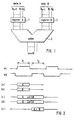
- An adder circuit is illustrated in Fig. 1.
- This circuit is well used in a data processing apparatus and has a register 1 storing a data A of n-bit length, a register 2 storing a data B of n-bit length and an adder 3.
- an adding operation is performed in accordance with a timing chart of Fig. 2.
- a period T 1 two data A and B are set in the registers 1 and 2, respectively, as shown in (a) and (b) of Fig. 2.
- This period is a data transmission period.
- a period T 2 is assigned to an adding operation as shown in (e) of Fig. 2.
- the registers 1 and 2 latch the respective data A and B in periods T 1 and T 2 as shown in (c) and (d) of Fig. 2.
- the adder performs an addition in bit parallel, a long period of time is required to the addition (period T 2 ) when a long bit length is manipulated, because a propagation delay time of a carry signal is long.
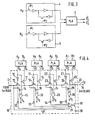
- the registers 1 and 2 of Fig. 1 have latches corresponding to a bit length of a data in number. For example, a bit Ao of the data A and a bit Bo of the data B are latched in the respective latches 4 and 5 of Fig. 3 and are applied to a decoding means 6 (a programmable logic array: PLA) in parallel.
- the PLA 6 decodes the input two bits Ao and Bo according to a predetermined logical algorithm shown in the following Table 1.
- the PLA can produce a sum of the bits Ao and Bo as shown in column SUM, that is the PLA 6 has an adding function of each bit and a carry signal producing function. Therefore, an adding operation is performed in accordance with outputs of the PLA 6.
- the adder 3 of Fig. 1 has a group of PLAs.
- a long data is divided into several blocks, for example a data of 32 bits is divided into 8 blocks each of which has 4 bits.
- a carry circuit corresponding to one of these 8 blocks is shown in Fig. 4.
- Fig. 4 shows a 2nd block 10 which includes bits A4 to A 7 and bits B 4 to B 7 and receives SUM signats S 4 to S 7 and CARRY signals C 4 to C 7 .
- the block 10 has four same stages each of which includes an inverter 12 (17, 22, 27) inverting the signal S 4 ( S 5 , S 6 , S 7 ), a switching transistor 11 (16, 21, 26), a transfer gate transistor 13 (18, 23, 28), an inverter 14 (19, 24, 29) and an exclusive NOR circuit 15 (20, 25, 30).
- a carry signal from the 1st stage is propagated through a carry signal propagation line 40 to the 3rd stage.
- the transfer gate transistors 13, 18, 23 and 28 are inserted into the propagation line 40 in series.
- the CARRY signals C 4 to C 7 are coupled to the propagation line 40 when the respective switching transistor (11, 16, 21, 26) is turned on in response to the SUM signal ( S 4 to S 7 ).
- the exclusive NOR circuits 15, 20, 25 and 30 are used to produce SUM signals S 4 to S 7 at each bit positions by adding the SUM signals S 4 to S 7 to a carry signal from the previous bit portion. Now, it is assumed in this embodiment that "0" level signal is propagated when the carry signal exists, while "1" level signal is propagated when no carry signal exists. Therefore, the carry signal from the previous bit portion is applied to the exclusive NOR circuits through inverters 14, 19, 24 and 29, respectively.
- the transfer gate transistor 13 is turned off, while the switching transistor 11 is turned on.
- "0" level signal indicating existence of a carry signal from the bit portion (A4, B 4 ) is propagated to the following bit portion (A 5 , B o ).
- the exclusive NOR circuit 15 produces “1” when a carry signal from the 1st block is present, while it produces “0” when the carry signal from the 1st block is absent.
- the carry circuit having the block 10 of Fig. 4 is driven on the basis of the CLA method.
- each block can not execute the carry operation until the carry signal from the previous block is received or is settled. Therefore, if each block has a carry propagation delay time ( ⁇ t), at least 8 ⁇ t delay time is required in the adding period T 2 of Fig. 2.
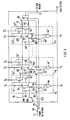
- FIG. 5 shows a second block 10' corresponding to Fig. 4.
- a carry propagation delay time (At) can be remarkably reduced.
- the block 10' includes four bit portions A4 to A 7 , in which A 6 is omitted. Each portion will be the same circuit design.
- the portion A4 includes two transfer gate transistors 50 and 51, four switching transistors 52 to 55 and an exclusive NOR circuit 56.
- a T 4 signal is directly applied to the exclusive NOR circuit 56 and is applied to the transfer gate transistors 50 and 51 via an inverter 57.
- One switching transistor 52 electrically couples a C 4 signal to a first propagation line 100 in response to the S 4 signal.
- the other switching transistor 53 electrically couples the C 4 signal to a second propagation line 101 in response to the S 4 signal.
- a first signal source 70 is coupled to an input end of the first propagation line 100 for supplying a "1" level signal.
- a second signal source 71 is coupled to an input end of the second propagation line 101 for supplying a "0" level signal.
- a V DD voltage source and a ground (GND) voltage source may be used as the first and second signal sources, respectively.
- the "1" level signal is propagated to a first selecting transistor 60 through the first transfer gate transistors 50, 50' and 50".
- the "0" level signal is propagated to a second selecting transistor 61 through the second transfer gate transistors 51,51' and 51".
- Buffer circuits 62 and 63 are used for buffering a propagation signal level, but may be omitted.
- the first and second propagation lines 100 and 101 are coupled to the other input end of the exclusive NOR circuit 56 via an inverter 58 and a third switching transistor 54 and an inverter 59 and a fourth switching transistor 55.
- a carry signal C 1 from the previous 1st block is applied to a first selecting line 102 via two inverters 80 and 81.
- An inverted signal of the carry signal C 1 is applied to a second selecting line 103 via the inverter 80.
- the first selecting line 102 is coupled to the third switching transistors 54, 54' and 54" and the first selecting transistor 60.
- the second selecting line 103 is coupled to the fourth switching transistor 55, 55' and 55" and the second selecting transistor 61.
- the first transfer gate transistor 50 and the first and third switching transistors 52 and 54 are valid. Since the first and second signal sources 70 and 71 supplies the fixed "1" and "0" level potential to the first and second propagation lines 100 and 101, respectively, regardless of the carry signal C 1 , the abovementioned two carry operations have been terminated before the carry signal C 1 from the 1st block arrives at the inverter 80. In other words, these two carry operations are performed as soon as the S 4 to S 7 signals and the C 4 to C 7 signals are applied to the four stages A4 to A 7 .
- a carry signal C 2 can be transferred to the 3rd block at a high-speed.
- the delay period of the 2nd block is only the sum of a transfer period of the carry signal on the lines 102 and 103 and a selecting period of the selecting transistors 60 and 61. Particularly, abovementioned two carry operations are performed within the data transfer period T 1 of Fig. 2. Therefore, the carry propagation delay time At is remarkably reduced.
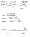
- Fig. 6 illustrates a carry circuit in a 32 bits adder and Fig. 7 shows a timing chart indicating a carry propagation delay time in Fig. 6.
- 8 blocks are required as shown in Fig. 6.
- a first block 200 is not received a carry signal at a carry input end, and therefore a delay period ⁇ T 1 , which is equal to the sum of delay times ⁇ So to AS 3 spent in the four bit portions (A o , B o to A3, B 3 ) is required.
- each carry operation is performed in a short delay time ⁇ t.
- total delay period is 8 ⁇ ⁇ T 1 , while it is only ⁇ T 1 +6 ⁇ t according to the embodiment shown in Fig. 6.
- Fig. 8 shows the carry circuit of another embodiment including a plurality of blocks.
- This carry circuit has a first carry block 300, a second carry block 301 coupled to the first block 300 via a buffer circuit 300a, and a third carry block 302 coupled to the second block 301 via a buffer circuit 301 a.
- Into the first block 300 are input the SUM signals of each bit S 1 to S 1+P and the CARRY signals C 1 to C 1+P , into the second block 301 the SUM signals S o to S n and the CARRY signals C o to C n , and into the third block 302 the SUM signals S "+ , to and the CARRY signals C n+ 1 to C n+m . respectively.
- a carry signal C 1 is obtained as a result of each delay At in each bit portion.
- the third block 302 may consist of 10 bits, because the arithmetic operation in the block 302 can be executed until the carry signal C 2 in the second block has been output, and this block 302 can process longer than the previous block 301 by AT, namely the process time for the two bits of sum signals S 24 , S25.
- This block 302 outputs a carry signal C 3 , to the following block after AT.
- each following block can execute arithmetic operation longer than its preceding block by ⁇ T, namely the time required for selecting operation of the transistors 60 and 61.
- the following block can not start a carry operation and a sum operation until a carry signal from the previous block has been applied thereto. While, according to the carry circuit shown in Fig. 6, each block can simultaneously start a carry operation and a sum operation because waiting a carry signal from the previous block is not necessary as shown in Fig. 7. With respect to the 1st block, since this block does not receive a carry signal, a first bit portion (A o , B o ) of the 1 st block may receive a "1" level signal indicating no carry signal. Therefore, the 1st block may have only the first propagation line 70 of Fig.
- each bit portion of the 1st block may have the inverter 57, the first transfer gate 50, the first switching transistor 52 and the exclusive NOR circuit 56. Therefore, the same operation period can be assigned to all of the 1st to 8th blocks. In other words, a carry operation for producing a carry signal from the each block and a sum operation for producing the result of the addition have been terminated in the same period if each block has the same bit portions.
- a selecting operation is added to the abovementioned two operations.
- the carry circuit shown in Fig. 8 can be provided.
- the number of divided blocks in an arithmetic operation of a long bit string (a long data) can be reduced.
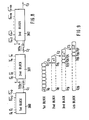
- Fig. 10 shows another embodiment of a preferred carry circuit to suit for an arithmetic operation of 64 bits.
- 4 bits are assigned to 1st to 4th blocks, respectively.
- 8 bits are assigned to 5th to 8th blocks, respectively.
- 16 bits are assigned to 9th block.
- Each carry operation time of 1st to 4th blocks is to, and each selecting period of these blocks is At o .
- the At o corresponds to 1 bit delay time of the carry operation
- the 5th block has a carry operation time t 1 equal to 8 bits delay time, so that the 5th block can manipulate 8 bits.
- the 9th block can manipulate 16 bits.
- a ⁇ t 1 is longer than the At o because the selecting lines 102 and 103 of the 5th block is longer than that of the 1st to 4th blocks.
- bits to be operated are assigned as shown in Fig. 10.
- a long data can be processed in a small number of blocks in accordance with a unit of bits to be transferred or to be accessed.
- the unit of bits is 4 bits per one address accessing.
Landscapes
- Physics & Mathematics (AREA)
- General Physics & Mathematics (AREA)
- Engineering & Computer Science (AREA)
- Computational Mathematics (AREA)
- Mathematical Analysis (AREA)
- Pure & Applied Mathematics (AREA)
- Theoretical Computer Science (AREA)
- Computing Systems (AREA)
- Mathematical Optimization (AREA)
- General Engineering & Computer Science (AREA)
- Compression, Expansion, Code Conversion, And Decoders (AREA)
- Logic Circuits (AREA)
Claims (1)
- Übertragsschaltung mit einer Vielzahl von Übertrags-Operationsstufen, wobei zumindest eine Stufe umfaßt ein erstes Übertragungstor (50), ein zweites Übertragungstor (51), ein erstes Schalttor (52), ein zweites Schalttor (53), eine ausschließende NOR-Schaltung (56), ein erstes Glied (100), das unabhängig versehen ist mit einem Übertragseingang (c1) zum Liefern eines ersten Signals (70) an einen Eingangsanschluß des ersten Übertragungstors (50), bevor an dem Übertragseingang (c1) ein Übertragssignal von der vorigen Stufe empfangen wird, ein zweites Glied (101), das unabhängig versehen ist mit einem Übertragseingang (c1) zum Liefern eines zweiten Signals (71) an einen Eingangsanschluß des zweiten Übertragungstors (51), bevor an dem Übertragseingang (c1) das Übertragssignal von der vorigen Stufe empfangen wird, ein Glied (57) zum Steuern des EIN- und AUS-Zustandes des ersten und zweiten Übertragungstores (50, 51) gemäß einem Summensignal (s4) aus zwei au addierenden Bits, wobei das Umkehrsignal des Summensignals (s4) an einen Eingangsanschluß der ausschließenden NOR-Schaltung (56) geliefert wird, einem Glied zum Liefern eines entsprechend einer Kombination aus zwei zu addierenden Bits erzeugten Umkehr-Übertragungssignals (c4) an Eingangsanschlüsse des ersten und zweiten Schalttores (52, 53), einem Glied zum Verbinden der Ausgangsanschlüsse des ersten und zweiten Schalttores (52, 53) an Ausgangsanschlüsse des ersten und zweiten Übertragungstores (50, 51), einem Glied zum Steuern des EIN- und AUS-Zustandes des ersten und zweiten Schalttores (52 und 53) entsprechend dem umgekehrten Signal des Summensignals (s4), einem Glied (60, 61, 80, 81) zum Wählen eines der Ausgangssignale des ersten und zweiten Übertragungstores (50, 51) entsprechend dem Übertragssignal (c1) von der vorigen Stufe, wobei das erste Glied (100) und das zweite Glied (101) wahlweise mit dem anderen Eingangsanschluß der ausschließenden NOR-Schaltung (56) über die Schalttore (54, 55) verbunden wird, in Abhängigkeit von dem Zustand des Übertragssignals (c1) von der vorigen Stufe, und einem Glied zum Übertragen des ausgewählten Ausgangssignals an die nachfolgende Stufe.
Applications Claiming Priority (4)
| Application Number | Priority Date | Filing Date | Title |
|---|---|---|---|
| JP25010583A JPS60140426A (ja) | 1983-12-27 | 1983-12-27 | キヤリ−回路 |
| JP250105/83 | 1983-12-27 | ||
| JP24700683A JPS60140425A (ja) | 1983-12-28 | 1983-12-28 | キヤリ−回路 |
| JP247006/83 | 1983-12-28 |
Publications (3)
| Publication Number | Publication Date |
|---|---|
| EP0164450A2 EP0164450A2 (de) | 1985-12-18 |
| EP0164450A3 EP0164450A3 (en) | 1986-04-23 |
| EP0164450B1 true EP0164450B1 (de) | 1990-03-07 |
Family
ID=26538015
Family Applications (1)
| Application Number | Title | Priority Date | Filing Date |
|---|---|---|---|
| EP84116331A Expired EP0164450B1 (de) | 1983-12-27 | 1984-12-27 | Eine, für eine arithmetische Operation hoher Geschwindigkeit geeignete, Übertragsschaltung |
Country Status (3)
| Country | Link |
|---|---|
| US (2) | US4763295A (de) |
| EP (1) | EP0164450B1 (de) |
| DE (1) | DE3481559D1 (de) |
Families Citing this family (17)
| Publication number | Priority date | Publication date | Assignee | Title |
|---|---|---|---|---|
| GB8531380D0 (en) * | 1985-12-20 | 1986-02-05 | Texas Instruments Ltd | Multi-stage parallel binary adder |
| US4737926A (en) * | 1986-01-21 | 1988-04-12 | Intel Corporation | Optimally partitioned regenerative carry lookahead adder |
| FR2596544B1 (fr) * | 1986-03-28 | 1988-05-13 | Radiotechnique Compelec | Circuit arithmetique et logique |
| FR2596543B1 (fr) * | 1986-03-28 | 1989-10-27 | Radiotechnique Compelec | Unite arithmetique et logique |
| EP0257362A1 (de) * | 1986-08-27 | 1988-03-02 | Siemens Aktiengesellschaft | Addierer |
| JPH07120271B2 (ja) * | 1987-04-28 | 1995-12-20 | 日本電気株式会社 | 算術論理装置 |
| FR2628232B1 (fr) * | 1988-03-07 | 1994-04-08 | Etat Francais Cnet | Additionneur de type recursif pour calculer la somme de deux operandes |
| JP2885402B2 (ja) * | 1988-06-15 | 1999-04-26 | 富士通株式会社 | 並列形全加算器の桁上げ伝搬回路 |
| US4982357A (en) * | 1989-04-28 | 1991-01-01 | International Business Machines Corporation | Plural dummy select chain logic synthesis network |
| US5301341A (en) * | 1990-11-28 | 1994-04-05 | International Business Machines Corporation | Overflow determination for three-operand alus in a scalable compound instruction set machine which compounds two arithmetic instructions |
| US5163019A (en) * | 1990-11-29 | 1992-11-10 | Brooktree Corporation | Binary carry circuitry |
| US5146424A (en) * | 1991-11-21 | 1992-09-08 | Unisys Corporation | Digital adder having a high-speed low-capacitance carry bypass signal path |
| EP0590251A2 (de) * | 1992-09-22 | 1994-04-06 | Motorola, Inc. | Hochgeschwindigkeitsaddierer |
| KR0137969Y1 (ko) * | 1993-03-26 | 1999-04-01 | 문정환 | 캐리전달회로 |
| KR950004225B1 (ko) * | 1993-04-16 | 1995-04-27 | 현대전자산업주식회사 | 고속 캐리 증가 가산기 |
| GB2342193B (en) | 1998-06-19 | 2003-06-04 | Sgs Thomson Microelectronics | Addition circuitry |
| US20060277243A1 (en) * | 2005-06-02 | 2006-12-07 | International Business Machines Corporation | Alternate representation of integers for efficient implementation of addition of a sequence of multiprecision integers |
Family Cites Families (9)
| Publication number | Priority date | Publication date | Assignee | Title |
|---|---|---|---|---|
| US3553446A (en) * | 1966-08-04 | 1971-01-05 | Honeywell Inc | Carry determination logic |
| US3717755A (en) * | 1971-05-21 | 1973-02-20 | Bell Telephone Labor Inc | Parallel adder using a carry propagation bus |
| US3728532A (en) * | 1972-01-21 | 1973-04-17 | Rca Corp | Carry skip-ahead network |
| US3843876A (en) * | 1973-09-20 | 1974-10-22 | Motorola Inc | Electronic digital adder having a high speed carry propagation line |
| US4031379A (en) * | 1976-02-23 | 1977-06-21 | Intel Corporation | Propagation line adder and method for binary addition |
| US4152775A (en) * | 1977-07-20 | 1979-05-01 | Intel Corporation | Single line propagation adder and method for binary addition |
| US4425623A (en) * | 1981-07-14 | 1984-01-10 | Rockwell International Corporation | Lookahead carry circuit apparatus |
| DE3138991A1 (de) * | 1981-09-30 | 1983-04-14 | Siemens AG, 1000 Berlin und 8000 München | Digitales rechenwerk und verfahren zu seinem betrieb |
| US4504924A (en) * | 1982-06-28 | 1985-03-12 | International Business Machines Corporation | Carry lookahead logical mechanism using affirmatively referenced transfer gates |
-
1984
- 1984-12-27 DE DE8484116331T patent/DE3481559D1/de not_active Expired - Lifetime
- 1984-12-27 US US06/686,802 patent/US4763295A/en not_active Expired - Lifetime
- 1984-12-27 EP EP84116331A patent/EP0164450B1/de not_active Expired
-
1988
- 1988-03-04 US US07/164,032 patent/US4845655A/en not_active Expired - Fee Related
Also Published As
| Publication number | Publication date |
|---|---|
| EP0164450A2 (de) | 1985-12-18 |
| US4763295A (en) | 1988-08-09 |
| US4845655A (en) | 1989-07-04 |
| DE3481559D1 (de) | 1990-04-12 |
| EP0164450A3 (en) | 1986-04-23 |
Similar Documents
| Publication | Publication Date | Title |
|---|---|---|
| EP0164450B1 (de) | Eine, für eine arithmetische Operation hoher Geschwindigkeit geeignete, Übertragsschaltung | |
| US5991209A (en) | Split sense amplifier and staging buffer for wide memory architecture | |
| EP0047440A1 (de) | Schiebeschaltung | |
| US4383304A (en) | Programmable bit shift circuit | |
| GB2117145A (en) | Memory control system | |
| EP0493835B1 (de) | Arithmetische Operationseinheit mit Bit-Invertierungsfunktion | |
| JPH061902B2 (ja) | プログラムド・ロジツク・アレイ | |
| US6317763B1 (en) | Circuits, barrel shifters, and methods of manipulating a bit pattern | |
| JPH0666682B2 (ja) | 集積回路構体 | |
| EP1406388A2 (de) | Integrierte Schaltungsanordnungen mit Dateninversion zur Verringerung von Störsignalen bei gleichzeitigem Schalten und Verschachtelung von Paralleldaten | |
| JPH0669813A (ja) | 可変長コードデコーディング装置 | |
| US5944775A (en) | Sum-of-products arithmetic unit | |
| EP0334103B1 (de) | Datenverarbeitungseinheit mit einem Umgehungsmechanismus | |
| US5416731A (en) | High-speed barrel shifter | |
| GB2401962A (en) | A sum bit generation circuit | |
| JPH0573268A (ja) | 加算器 | |
| CN1004306B (zh) | 信息处理装置 | |
| JPH0697431B2 (ja) | バレルシフタ | |
| EP0334131B1 (de) | Datenprozessor zur Durchführung einer Operation auf Daten mit einer Länge kürzer als ein Wort | |
| EP0271168B1 (de) | Dateneingangsauswahl | |
| JP3781573B2 (ja) | 論理回路 | |
| JP3038757B2 (ja) | シフトレジスタ回路 | |
| EP0354534B1 (de) | Halbleiter-Logikschaltung | |
| EP0496002A1 (de) | Registerschaltkreis | |
| KR100201030B1 (ko) | 이진-선택 인코더 네트워크 |
Legal Events
| Date | Code | Title | Description |
|---|---|---|---|
| PUAI | Public reference made under article 153(3) epc to a published international application that has entered the european phase |
Free format text: ORIGINAL CODE: 0009012 |
|
| 17P | Request for examination filed |
Effective date: 19841227 |
|
| AK | Designated contracting states |
Designated state(s): DE FR GB |
|
| PUAL | Search report despatched |
Free format text: ORIGINAL CODE: 0009013 |
|
| AK | Designated contracting states |
Kind code of ref document: A3 Designated state(s): DE FR GB |
|
| 17Q | First examination report despatched |
Effective date: 19871120 |
|
| GRAA | (expected) grant |
Free format text: ORIGINAL CODE: 0009210 |
|
| AK | Designated contracting states |
Kind code of ref document: B1 Designated state(s): DE FR GB |
|
| REF | Corresponds to: |
Ref document number: 3481559 Country of ref document: DE Date of ref document: 19900412 |
|
| ET | Fr: translation filed | ||
| PLBE | No opposition filed within time limit |
Free format text: ORIGINAL CODE: 0009261 |
|
| STAA | Information on the status of an ep patent application or granted ep patent |
Free format text: STATUS: NO OPPOSITION FILED WITHIN TIME LIMIT |
|
| 26N | No opposition filed | ||
| PGFP | Annual fee paid to national office [announced via postgrant information from national office to epo] |
Ref country code: FR Payment date: 19991208 Year of fee payment: 16 |
|
| PGFP | Annual fee paid to national office [announced via postgrant information from national office to epo] |
Ref country code: GB Payment date: 19991222 Year of fee payment: 16 |
|
| PGFP | Annual fee paid to national office [announced via postgrant information from national office to epo] |
Ref country code: DE Payment date: 19991230 Year of fee payment: 16 |
|
| PG25 | Lapsed in a contracting state [announced via postgrant information from national office to epo] |
Ref country code: GB Free format text: LAPSE BECAUSE OF NON-PAYMENT OF DUE FEES Effective date: 20001227 |
|
| GBPC | Gb: european patent ceased through non-payment of renewal fee |
Effective date: 20001227 |
|
| PG25 | Lapsed in a contracting state [announced via postgrant information from national office to epo] |
Ref country code: FR Free format text: LAPSE BECAUSE OF NON-PAYMENT OF DUE FEES Effective date: 20010831 |
|
| REG | Reference to a national code |
Ref country code: FR Ref legal event code: ST |
|
| PG25 | Lapsed in a contracting state [announced via postgrant information from national office to epo] |
Ref country code: DE Free format text: LAPSE BECAUSE OF NON-PAYMENT OF DUE FEES Effective date: 20011002 |