EP0164517A1 - Transistors à hétérojonction - Google Patents
Transistors à hétérojonction Download PDFInfo
- Publication number
- EP0164517A1 EP0164517A1 EP85104227A EP85104227A EP0164517A1 EP 0164517 A1 EP0164517 A1 EP 0164517A1 EP 85104227 A EP85104227 A EP 85104227A EP 85104227 A EP85104227 A EP 85104227A EP 0164517 A1 EP0164517 A1 EP 0164517A1
- Authority
- EP
- European Patent Office
- Prior art keywords
- region
- collector
- base
- electrode
- contact
- Prior art date
- Legal status (The legal status is an assumption and is not a legal conclusion. Google has not performed a legal analysis and makes no representation as to the accuracy of the status listed.)
- Granted
Links
Images
Classifications
-
- H—ELECTRICITY
- H10—SEMICONDUCTOR DEVICES; ELECTRIC SOLID-STATE DEVICES NOT OTHERWISE PROVIDED FOR
- H10D—INORGANIC ELECTRIC SEMICONDUCTOR DEVICES
- H10D10/00—Bipolar junction transistors [BJT]
- H10D10/40—Vertical BJTs
- H10D10/461—Inverted vertical BJTs
-
- H—ELECTRICITY
- H10—SEMICONDUCTOR DEVICES; ELECTRIC SOLID-STATE DEVICES NOT OTHERWISE PROVIDED FOR
- H10D—INORGANIC ELECTRIC SEMICONDUCTOR DEVICES
- H10D10/00—Bipolar junction transistors [BJT]
- H10D10/80—Heterojunction BJTs
- H10D10/821—Vertical heterojunction BJTs
-
- H—ELECTRICITY
- H10—SEMICONDUCTOR DEVICES; ELECTRIC SOLID-STATE DEVICES NOT OTHERWISE PROVIDED FOR
- H10D—INORGANIC ELECTRIC SEMICONDUCTOR DEVICES
- H10D30/00—Field-effect transistors [FET]
- H10D30/60—Insulated-gate field-effect transistors [IGFET]
- H10D30/67—Thin-film transistors [TFT]
- H10D30/6729—Thin-film transistors [TFT] characterised by the electrodes
- H10D30/6737—Thin-film transistors [TFT] characterised by the electrodes characterised by the electrode materials
- H10D30/6738—Schottky barrier electrodes
-
- H—ELECTRICITY
- H10—SEMICONDUCTOR DEVICES; ELECTRIC SOLID-STATE DEVICES NOT OTHERWISE PROVIDED FOR
- H10D—INORGANIC ELECTRIC SEMICONDUCTOR DEVICES
- H10D30/00—Field-effect transistors [FET]
- H10D30/60—Insulated-gate field-effect transistors [IGFET]
- H10D30/67—Thin-film transistors [TFT]
- H10D30/674—Thin-film transistors [TFT] characterised by the active materials
- H10D30/675—Group III-V materials, Group II-VI materials, Group IV-VI materials, selenium or tellurium
-
- H—ELECTRICITY
- H10—SEMICONDUCTOR DEVICES; ELECTRIC SOLID-STATE DEVICES NOT OTHERWISE PROVIDED FOR
- H10D—INORGANIC ELECTRIC SEMICONDUCTOR DEVICES
- H10D62/00—Semiconductor bodies, or regions thereof, of devices having potential barriers
- H10D62/80—Semiconductor bodies, or regions thereof, of devices having potential barriers characterised by the materials
- H10D62/85—Semiconductor bodies, or regions thereof, of devices having potential barriers characterised by the materials being Group III-V materials, e.g. GaAs
-
- H—ELECTRICITY
- H10—SEMICONDUCTOR DEVICES; ELECTRIC SOLID-STATE DEVICES NOT OTHERWISE PROVIDED FOR
- H10D—INORGANIC ELECTRIC SEMICONDUCTOR DEVICES
- H10D64/00—Electrodes of devices having potential barriers
- H10D64/20—Electrodes characterised by their shapes, relative sizes or dispositions
- H10D64/27—Electrodes not carrying the current to be rectified, amplified, oscillated or switched, e.g. gates
- H10D64/281—Base electrodes for bipolar transistors
-
- H—ELECTRICITY
- H10—SEMICONDUCTOR DEVICES; ELECTRIC SOLID-STATE DEVICES NOT OTHERWISE PROVIDED FOR
- H10D—INORGANIC ELECTRIC SEMICONDUCTOR DEVICES
- H10D64/00—Electrodes of devices having potential barriers
- H10D64/60—Electrodes characterised by their materials
- H10D64/62—Electrodes ohmically coupled to a semiconductor
-
- H—ELECTRICITY
- H10—SEMICONDUCTOR DEVICES; ELECTRIC SOLID-STATE DEVICES NOT OTHERWISE PROVIDED FOR
- H10D—INORGANIC ELECTRIC SEMICONDUCTOR DEVICES
- H10D64/00—Electrodes of devices having potential barriers
- H10D64/60—Electrodes characterised by their materials
- H10D64/64—Electrodes comprising a Schottky barrier to a semiconductor
-
- Y—GENERAL TAGGING OF NEW TECHNOLOGICAL DEVELOPMENTS; GENERAL TAGGING OF CROSS-SECTIONAL TECHNOLOGIES SPANNING OVER SEVERAL SECTIONS OF THE IPC; TECHNICAL SUBJECTS COVERED BY FORMER USPC CROSS-REFERENCE ART COLLECTIONS [XRACs] AND DIGESTS
- Y10—TECHNICAL SUBJECTS COVERED BY FORMER USPC
- Y10S—TECHNICAL SUBJECTS COVERED BY FORMER USPC CROSS-REFERENCE ART COLLECTIONS [XRACs] AND DIGESTS
- Y10S148/00—Metal treatment
- Y10S148/01—Bipolar transistors-ion implantation
-
- Y—GENERAL TAGGING OF NEW TECHNOLOGICAL DEVELOPMENTS; GENERAL TAGGING OF CROSS-SECTIONAL TECHNOLOGIES SPANNING OVER SEVERAL SECTIONS OF THE IPC; TECHNICAL SUBJECTS COVERED BY FORMER USPC CROSS-REFERENCE ART COLLECTIONS [XRACs] AND DIGESTS
- Y10—TECHNICAL SUBJECTS COVERED BY FORMER USPC
- Y10S—TECHNICAL SUBJECTS COVERED BY FORMER USPC CROSS-REFERENCE ART COLLECTIONS [XRACs] AND DIGESTS
- Y10S148/00—Metal treatment
- Y10S148/084—Ion implantation of compound devices
-
- Y—GENERAL TAGGING OF NEW TECHNOLOGICAL DEVELOPMENTS; GENERAL TAGGING OF CROSS-SECTIONAL TECHNOLOGIES SPANNING OVER SEVERAL SECTIONS OF THE IPC; TECHNICAL SUBJECTS COVERED BY FORMER USPC CROSS-REFERENCE ART COLLECTIONS [XRACs] AND DIGESTS
- Y10—TECHNICAL SUBJECTS COVERED BY FORMER USPC
- Y10S—TECHNICAL SUBJECTS COVERED BY FORMER USPC CROSS-REFERENCE ART COLLECTIONS [XRACs] AND DIGESTS
- Y10S148/00—Metal treatment
- Y10S148/14—Schottky barrier contacts
Definitions
- This invention relates to heterojunction transistors.
- heterojunction transistors made of more than one type of semiconductor material are known as heterojunction transistors. Such materials are usually of the intermetallic type such as gallium arsenide and gallium aluminum arsenide. These materials have some advantageous properties and some properties that require special consideration in use. In bipolar transistor structures, the size of the extrinsic base region may cause the base resistance to be higher than desirable and efforts to compensate usually involve positioning the base contact very close to either the collector electrode or the emitter electrode. Heterojunction transistors are also susceptible to saturation and steps must be taken to either prevent or control it.
- US-A-3,938,243 discloses a technique of saturation control in silicon devices by means of a metal electrode that bridges two regions but provides different impedances to the two regions.
- a heterojunction transistor is characterised, in accordance with the invention, in that it includes an electrode bridging and making contact with both the base region and either the collector region or the emitter region, the electrode and the regions of the transistor with which it makes contact being of such materials that the electrode forms an ohmic contact with the base region and a Schottky barrier contact with the collector region or the emitter region.
- the invention involves the use of a specific type of electrode over the interface of the collector or emitter and the base region of a heterojunction transistor which when in place operates to serve the combined functions of a base electrode closely spaced to a junction and a Schottky barrier saturation control clamp between the base and either the emitter or collector of the transistor.
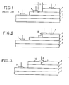
- FIG. 1 represents a known type of heterojunction transistor which typically has a substrate 1 of gallium arsenide.
- an n emitter region 2 of for example GaAlAs.
- An ohmic emitter electrode 3 is provided to the emitter region 2.
- a base region 4 of for example p-type GaAs or p-type graded GaAlAs.
- An ohmic base electrode contact 5 is provided to the base region 4.
- a collector region 6 of n-type semiconductor material which is different from that of the base region 4 so that a heterojunction is formed.
- the collector region may be of GaAlAs or GaAs.
- An ohmic collector electrode contact 7 is provided to the region 6.
- an electrode 8 of a selected metal is placed over the interface of the base region and the collector region.
- the metal electrode 8 forms an ohmic contact with the base region and forms a Schottky barrier contact with the collector region.
- the metal electrode 8 further serves as the combination of a closely spaced base contact coupled with a built-in collector-to-base Schottky barrier clamp.
- an n substrate is epitaxially joined to an n emitter 2 provided with an ohmic emitter contact 3.
- An epitaxial region 4 and a collector 6 forming a heterocollector junction are provided.
- An ohmic collector contact 7 is also provided.
- transistors may operate with a common emitter and hence may not have the contact 3.
- the point of departure for the invention is the contact 8, positioned across the interface between the base 4 and the collector 6, which forms both an ohmic contact with the base region 4 and a Schottky barrier contact with the collector region 6. Since the ohmic contact with the base region 4 is at the interface between the collector region 6 and the base region 4 it is at the minimum spacing and because of the Schottky barrier impedance with the collector 6, no processing accommodation need be made to prevent shorting.
- the electrode also serves as a clamp for the transistor. As the saturation condition is approached, the base region of these devices would reach a potential with respect to either the emitter or collector that is opposite to the normal potential but such situation is prevented because the Schottky barrier portion of the electrode of the invention at that point becomes forward biased.
- FIG. 3 an alternative embodiment of the invention is illustrated where a portion of the collector region 6 is converted, for example by ion implantation, to the same conductivity type as the base 4 and the electrode 8 positioned across the interface 9 forms an ohmic contact with the converted region 10 and a Schottky barrier rectifying contact with the region 6. While the conversion is shown for illustration as ending at an interface between layers, in practice it may penetrate as far as desired. All other reference numerals indicate items corresponding to those in the structures of the other Figures.
- the preferred method of carrying out the invention involves providing for the region 1 an n + GaAs substrate doped to approximately 10 18 atoms per cm 3 .
- the n-type GaAlAs emitter would be doped with silicon to about 10 17 atoms per cm 3 .
- the p-type base 4 would be doped with beryllium or magnesium to about 10 18 atoms per cm 3 , providing a 10 -2 ohm-cm base resistance.
- the n-type collector 6 of GaAs would be doped to about 10 17 atoms per cm3 with silicon.
- the base collector contact 8 would be made of palladium, platinum or nickel and their silicides sintered at an approximate temperature of about 500°C.
- the electrodes 3 and 7 would be conventional ohmic connections such as AuGe.
- the electrode 8 provides a simple solution to two well known problems.
- the preferred embodiments employs the intermetallic semiconductor materials GaAs and alloys thereof, it will be apparent that a number of semiconductor materials, such as GaInAs, AlInAs, GaInAl and InP, and suitable metal electrodes may be used.
- the metal electrode may alternatively be arranged to serve as a saturation clamp on the emitter, although the more prevalent use is as described above for a collector saturation clamp.
- an electrode that serves as a combined base to collector or base to emitter contact forming an ohmic contact to the base at the interface where the collector or emitter region joins the base and extends over the collector or emitter region forming a Schottky barrier contact thereto so that both a minimum spaced ohmic base to collector or emitter to base, contact is provided, together with a Schottky collector or emitter clamp for a heterojunction transistor.
Landscapes
- Bipolar Transistors (AREA)
- Electrodes Of Semiconductors (AREA)
Applications Claiming Priority (2)
| Application Number | Priority Date | Filing Date | Title |
|---|---|---|---|
| US609406 | 1984-05-11 | ||
| US06/609,406 US4586071A (en) | 1984-05-11 | 1984-05-11 | Heterostructure bipolar transistor |
Publications (2)
| Publication Number | Publication Date |
|---|---|
| EP0164517A1 true EP0164517A1 (fr) | 1985-12-18 |
| EP0164517B1 EP0164517B1 (fr) | 1989-11-29 |
Family
ID=24440677
Family Applications (1)
| Application Number | Title | Priority Date | Filing Date |
|---|---|---|---|
| EP85104227A Expired EP0164517B1 (fr) | 1984-05-11 | 1985-04-11 | Transistors à hétérojonction |
Country Status (4)
| Country | Link |
|---|---|
| US (1) | US4586071A (fr) |
| EP (1) | EP0164517B1 (fr) |
| JP (1) | JPH0732160B2 (fr) |
| DE (1) | DE3574529D1 (fr) |
Cited By (3)
| Publication number | Priority date | Publication date | Assignee | Title |
|---|---|---|---|---|
| EP0507454A1 (fr) * | 1991-03-06 | 1992-10-07 | Kabushiki Kaisha Toshiba | Transistor bipolaire à hétérojonction et procédé pour sa fabrication |
| EP0472262B1 (fr) * | 1990-03-30 | 1997-12-10 | Kabushiki Kaisha Toshiba | Transistor bipolaire à hétérojonction |
| CN110752256A (zh) * | 2019-10-22 | 2020-02-04 | 深圳第三代半导体研究院 | 一种碳化硅肖特基钳位晶体管及其制备方法 |
Families Citing this family (14)
| Publication number | Priority date | Publication date | Assignee | Title |
|---|---|---|---|---|
| JPH0626242B2 (ja) * | 1983-12-05 | 1994-04-06 | 富士通株式会社 | 半導体集積回路装置 |
| JPH0614536B2 (ja) * | 1985-09-17 | 1994-02-23 | 株式会社東芝 | バイポ−ラ集積回路 |
| US4872040A (en) * | 1987-04-23 | 1989-10-03 | International Business Machines Corporation | Self-aligned heterojunction transistor |
| US4833517A (en) * | 1987-04-27 | 1989-05-23 | International Business Machines Corporation | Theta device with improved base contact |
| US4835580A (en) * | 1987-04-30 | 1989-05-30 | Texas Instruments Incorporated | Schottky barrier diode and method |
| JP2619407B2 (ja) * | 1987-08-24 | 1997-06-11 | 株式会社日立製作所 | 半導体装置の製造方法 |
| US4821082A (en) * | 1987-10-30 | 1989-04-11 | International Business Machines Corporation | Heterojunction bipolar transistor with substantially aligned energy levels |
| US4871686A (en) * | 1988-03-28 | 1989-10-03 | Motorola, Inc. | Integrated Schottky diode and transistor |
| US4981807A (en) * | 1988-10-31 | 1991-01-01 | International Business Machines Corporation | Process for fabricating complementary vertical transistor memory cell |
| US4939562A (en) * | 1989-04-07 | 1990-07-03 | Raytheon Company | Heterojunction bipolar transistors and method of manufacture |
| KR20070032824A (ko) * | 2004-07-20 | 2007-03-22 | 코닌클리즈케 필립스 일렉트로닉스 엔.브이. | 반도체 디바이스 및 그 제조 방법 |
| KR20070026826A (ko) * | 2004-07-20 | 2007-03-08 | 코닌클리즈케 필립스 일렉트로닉스 엔.브이. | 반도체 디바이스 및 그 제조 방법 |
| CN111081769B (zh) * | 2019-12-17 | 2025-02-11 | 中证博芯(重庆)半导体有限公司 | NPN型肖特基集电区AlGaN/GaN HBT器件及其制备方法 |
| CN110797402B (zh) * | 2019-12-17 | 2025-02-14 | 中证博芯(重庆)半导体有限公司 | PNP型肖特基集电区AlGaN/GaN HBT器件及其制备方法 |
Citations (2)
| Publication number | Priority date | Publication date | Assignee | Title |
|---|---|---|---|---|
| US3780359A (en) * | 1971-12-20 | 1973-12-18 | Ibm | Bipolar transistor with a heterojunction emitter and a method fabricating the same |
| US3938243A (en) * | 1973-02-20 | 1976-02-17 | Signetics Corporation | Schottky barrier diode semiconductor structure and method |
Family Cites Families (9)
| Publication number | Priority date | Publication date | Assignee | Title |
|---|---|---|---|---|
| JPS4943583A (fr) * | 1972-08-30 | 1974-04-24 | ||
| US3943554A (en) * | 1973-07-30 | 1976-03-09 | Signetics Corporation | Threshold switching integrated circuit and method for forming the same |
| US4005469A (en) * | 1975-06-20 | 1977-01-25 | International Business Machines Corporation | P-type-epitaxial-base transistor with base-collector Schottky diode clamp |
| JPS546777A (en) * | 1977-06-17 | 1979-01-19 | Nec Corp | Field effect type transistor |
| US4379005A (en) * | 1979-10-26 | 1983-04-05 | International Business Machines Corporation | Semiconductor device fabrication |
| JPS56133874A (en) * | 1980-03-22 | 1981-10-20 | Semiconductor Res Found | Semiconductor device |
| JPS57166068A (en) * | 1981-04-07 | 1982-10-13 | Toshiba Corp | Semiconductor device |
| JPS57176762A (en) * | 1981-04-22 | 1982-10-30 | Nec Corp | Semiconductor device |
| JPS5821866A (ja) * | 1981-07-31 | 1983-02-08 | Toshiba Corp | 半導体装置 |
-
1984
- 1984-05-11 US US06/609,406 patent/US4586071A/en not_active Expired - Fee Related
-
1985
- 1985-01-14 JP JP60003412A patent/JPH0732160B2/ja not_active Expired - Lifetime
- 1985-04-11 DE DE8585104227T patent/DE3574529D1/de not_active Expired - Lifetime
- 1985-04-11 EP EP85104227A patent/EP0164517B1/fr not_active Expired
Patent Citations (2)
| Publication number | Priority date | Publication date | Assignee | Title |
|---|---|---|---|---|
| US3780359A (en) * | 1971-12-20 | 1973-12-18 | Ibm | Bipolar transistor with a heterojunction emitter and a method fabricating the same |
| US3938243A (en) * | 1973-02-20 | 1976-02-17 | Signetics Corporation | Schottky barrier diode semiconductor structure and method |
Non-Patent Citations (1)
| Title |
|---|
| ELECTRONICS LETTERS, vol. 16, no. 1, January 1980, Hitchin, GB; D. ANKRI et al. "Design and evaluation of a planar GaAIAs-GaAs bipolar transistor", pages 41-42 * |
Cited By (4)
| Publication number | Priority date | Publication date | Assignee | Title |
|---|---|---|---|---|
| EP0472262B1 (fr) * | 1990-03-30 | 1997-12-10 | Kabushiki Kaisha Toshiba | Transistor bipolaire à hétérojonction |
| EP0507454A1 (fr) * | 1991-03-06 | 1992-10-07 | Kabushiki Kaisha Toshiba | Transistor bipolaire à hétérojonction et procédé pour sa fabrication |
| US5331186A (en) * | 1991-03-06 | 1994-07-19 | Kabushiki Kaisha Toshiba | Heterojunction bipolar transistor with base electrode having Schottky barrier contact to the emitter |
| CN110752256A (zh) * | 2019-10-22 | 2020-02-04 | 深圳第三代半导体研究院 | 一种碳化硅肖特基钳位晶体管及其制备方法 |
Also Published As
| Publication number | Publication date |
|---|---|
| JPS60241262A (ja) | 1985-11-30 |
| EP0164517B1 (fr) | 1989-11-29 |
| DE3574529D1 (de) | 1990-01-04 |
| US4586071A (en) | 1986-04-29 |
| JPH0732160B2 (ja) | 1995-04-10 |
Similar Documents
| Publication | Publication Date | Title |
|---|---|---|
| EP0164517B1 (fr) | Transistors à hétérojonction | |
| EP0562272A2 (fr) | Transistors bipolaires hyperfréquence à hétérojonction ayant les émetteurs conçus par l'utilisation en haute puissance et méthode pour les fabriquer | |
| US5124270A (en) | Bipolar transistor having external base region | |
| EP0184016A1 (fr) | Transistor bipolaire à hétérojonction | |
| EP0256360A2 (fr) | Diode tunnel commandée | |
| TW201513290A (zh) | 具有非金歐姆接點的砷化鎵爲基的裝置 | |
| EP0177246B1 (fr) | Transistor bipolaire à hétérojonction et procédé de fabrication | |
| US6462362B1 (en) | Heterojunction bipolar transistor having prevention layer between base and emitter | |
| EP1291923B1 (fr) | Transistor bipolaire à hétérojonction et procédé pour sa fabrication | |
| US4979009A (en) | Heterojunction bipolar transistor | |
| US6873029B2 (en) | Self-aligned bipolar transistor | |
| US4910562A (en) | Field induced base transistor | |
| US6133594A (en) | Compound semiconductor device | |
| EP0384113A2 (fr) | Transistor bipolaire à hétérojonction à base multicouche | |
| JPH05136159A (ja) | ヘテロ接合型バイポーラトランジスタ及びその製造方法 | |
| US4812886A (en) | Multilayer contact apparatus and method | |
| Yanagihara et al. | 253-GHz f/sub max/AlGaAs/GaAs HBT with Ni/Ti/Pt/Ti/Pt-contact and L-shaped base electrode | |
| US5376822A (en) | Heterojunction type of compound semiconductor integrated circuit | |
| EP0472262B1 (fr) | Transistor bipolaire à hétérojonction | |
| JP3235574B2 (ja) | ヘテロバイポーラトランジスタを有する半導体装置の製造方法 | |
| JPH0513377B2 (fr) | ||
| JP2714096B2 (ja) | 半導体装置およびその製造方法 | |
| JP2906407B2 (ja) | 半導体装置 | |
| KR100347520B1 (ko) | 이종접합 쌍극자 소자 및 그 제조방법 | |
| JP4405060B2 (ja) | ヘテロ接合型バイポーラトランジスタ |
Legal Events
| Date | Code | Title | Description |
|---|---|---|---|
| PUAI | Public reference made under article 153(3) epc to a published international application that has entered the european phase |
Free format text: ORIGINAL CODE: 0009012 |
|
| AK | Designated contracting states |
Designated state(s): DE FR GB |
|
| 17P | Request for examination filed |
Effective date: 19860325 |
|
| 17Q | First examination report despatched |
Effective date: 19871002 |
|
| GRAA | (expected) grant |
Free format text: ORIGINAL CODE: 0009210 |
|
| AK | Designated contracting states |
Kind code of ref document: B1 Designated state(s): DE FR GB |
|
| REF | Corresponds to: |
Ref document number: 3574529 Country of ref document: DE Date of ref document: 19900104 |
|
| ET | Fr: translation filed | ||
| PLBE | No opposition filed within time limit |
Free format text: ORIGINAL CODE: 0009261 |
|
| PLBE | No opposition filed within time limit |
Free format text: ORIGINAL CODE: 0009261 |
|
| STAA | Information on the status of an ep patent application or granted ep patent |
Free format text: STATUS: NO OPPOSITION FILED WITHIN TIME LIMIT |
|
| 26N | No opposition filed | ||
| 26N | No opposition filed | ||
| PGFP | Annual fee paid to national office [announced via postgrant information from national office to epo] |
Ref country code: FR Payment date: 19950328 Year of fee payment: 11 |
|
| PGFP | Annual fee paid to national office [announced via postgrant information from national office to epo] |
Ref country code: DE Payment date: 19950428 Year of fee payment: 11 |
|
| PG25 | Lapsed in a contracting state [announced via postgrant information from national office to epo] |
Ref country code: FR Effective date: 19961227 |
|
| PG25 | Lapsed in a contracting state [announced via postgrant information from national office to epo] |
Ref country code: DE Effective date: 19970101 |
|
| REG | Reference to a national code |
Ref country code: FR Ref legal event code: ST |
|
| PGFP | Annual fee paid to national office [announced via postgrant information from national office to epo] |
Ref country code: GB Payment date: 19970325 Year of fee payment: 13 |
|
| PG25 | Lapsed in a contracting state [announced via postgrant information from national office to epo] |
Ref country code: GB Free format text: LAPSE BECAUSE OF NON-PAYMENT OF DUE FEES Effective date: 19980411 |
|
| GBPC | Gb: european patent ceased through non-payment of renewal fee |
Effective date: 19980411 |