EP0164604A2 - Elément amplificateur intégré à émission et réception de lumière - Google Patents
Elément amplificateur intégré à émission et réception de lumière Download PDFInfo
- Publication number
- EP0164604A2 EP0164604A2 EP85106017A EP85106017A EP0164604A2 EP 0164604 A2 EP0164604 A2 EP 0164604A2 EP 85106017 A EP85106017 A EP 85106017A EP 85106017 A EP85106017 A EP 85106017A EP 0164604 A2 EP0164604 A2 EP 0164604A2
- Authority
- EP
- European Patent Office
- Prior art keywords
- phototransistor
- layer
- conductivity type
- semiconductor laser
- semiconductor
- Prior art date
- Legal status (The legal status is an assumption and is not a legal conclusion. Google has not performed a legal analysis and makes no representation as to the accuracy of the status listed.)
- Granted
Links
- 239000004065 semiconductor Substances 0.000 claims abstract description 54
- 239000000758 substrate Substances 0.000 claims abstract description 17
- 238000002347 injection Methods 0.000 claims description 3
- 239000007924 injection Substances 0.000 claims description 3
- 238000004519 manufacturing process Methods 0.000 abstract description 5
- 230000003287 optical effect Effects 0.000 description 14
- 238000000034 method Methods 0.000 description 10
- 229910000530 Gallium indium arsenide Inorganic materials 0.000 description 4
- 230000015572 biosynthetic process Effects 0.000 description 4
- 238000010586 diagram Methods 0.000 description 4
- 239000000463 material Substances 0.000 description 4
- 230000000903 blocking effect Effects 0.000 description 3
- 238000005530 etching Methods 0.000 description 3
- 239000012535 impurity Substances 0.000 description 3
- 239000000203 mixture Substances 0.000 description 3
- 230000004888 barrier function Effects 0.000 description 2
- 238000004891 communication Methods 0.000 description 2
- 239000000470 constituent Substances 0.000 description 2
- 238000007796 conventional method Methods 0.000 description 2
- 230000010354 integration Effects 0.000 description 2
- 230000031700 light absorption Effects 0.000 description 2
- 230000010355 oscillation Effects 0.000 description 2
- 239000012071 phase Substances 0.000 description 2
- 239000000243 solution Substances 0.000 description 2
- 229910001218 Gallium arsenide Inorganic materials 0.000 description 1
- 230000001419 dependent effect Effects 0.000 description 1
- 238000009792 diffusion process Methods 0.000 description 1
- 125000005842 heteroatom Chemical group 0.000 description 1
- DKAGJZJALZXOOV-UHFFFAOYSA-N hydrate;hydrochloride Chemical compound O.Cl DKAGJZJALZXOOV-UHFFFAOYSA-N 0.000 description 1
- 239000007791 liquid phase Substances 0.000 description 1
- 229920002120 photoresistant polymer Polymers 0.000 description 1
- 238000000926 separation method Methods 0.000 description 1
Images


Classifications
-
- H—ELECTRICITY
- H01—ELECTRIC ELEMENTS
- H01S—DEVICES USING THE PROCESS OF LIGHT AMPLIFICATION BY STIMULATED EMISSION OF RADIATION [LASER] TO AMPLIFY OR GENERATE LIGHT; DEVICES USING STIMULATED EMISSION OF ELECTROMAGNETIC RADIATION IN WAVE RANGES OTHER THAN OPTICAL
- H01S5/00—Semiconductor lasers
- H01S5/02—Structural details or components not essential to laser action
- H01S5/026—Monolithically integrated components, e.g. waveguides, monitoring photo-detectors, drivers
- H01S5/0262—Photo-diodes, e.g. transceiver devices, bidirectional devices
-
- H—ELECTRICITY
- H01—ELECTRIC ELEMENTS
- H01S—DEVICES USING THE PROCESS OF LIGHT AMPLIFICATION BY STIMULATED EMISSION OF RADIATION [LASER] TO AMPLIFY OR GENERATE LIGHT; DEVICES USING STIMULATED EMISSION OF ELECTROMAGNETIC RADIATION IN WAVE RANGES OTHER THAN OPTICAL
- H01S5/00—Semiconductor lasers
- H01S5/20—Structure or shape of the semiconductor body to guide the optical wave ; Confining structures perpendicular to the optical axis, e.g. index or gain guiding, stripe geometry, broad area lasers, gain tailoring, transverse or lateral reflectors, special cladding structures, MQW barrier reflection layers
- H01S5/22—Structure or shape of the semiconductor body to guide the optical wave ; Confining structures perpendicular to the optical axis, e.g. index or gain guiding, stripe geometry, broad area lasers, gain tailoring, transverse or lateral reflectors, special cladding structures, MQW barrier reflection layers having a ridge or stripe structure
- H01S5/227—Buried mesa structure ; Striped active layer
- H01S5/2275—Buried mesa structure ; Striped active layer mesa created by etching
- H01S5/2277—Buried mesa structure ; Striped active layer mesa created by etching double channel planar buried heterostructure [DCPBH] laser
-
- H—ELECTRICITY
- H03—ELECTRONIC CIRCUITRY
- H03K—PULSE TECHNIQUE
- H03K17/00—Electronic switching or gating, i.e. not by contact-making and –breaking
- H03K17/94—Electronic switching or gating, i.e. not by contact-making and –breaking characterised by the way in which the control signals are generated
- H03K17/941—Electronic switching or gating, i.e. not by contact-making and –breaking characterised by the way in which the control signals are generated using an optical detector
-
- H—ELECTRICITY
- H10—SEMICONDUCTOR DEVICES; ELECTRIC SOLID-STATE DEVICES NOT OTHERWISE PROVIDED FOR
- H10F—INORGANIC SEMICONDUCTOR DEVICES SENSITIVE TO INFRARED RADIATION, LIGHT, ELECTROMAGNETIC RADIATION OF SHORTER WAVELENGTH OR CORPUSCULAR RADIATION
- H10F55/00—Radiation-sensitive semiconductor devices covered by groups H10F10/00, H10F19/00 or H10F30/00 being structurally associated with electric light sources and electrically or optically coupled thereto
- H10F55/10—Radiation-sensitive semiconductor devices covered by groups H10F10/00, H10F19/00 or H10F30/00 being structurally associated with electric light sources and electrically or optically coupled thereto wherein the radiation-sensitive semiconductor devices control the electric light source, e.g. image converters, image amplifiers or image storage devices
- H10F55/15—Radiation-sensitive semiconductor devices covered by groups H10F10/00, H10F19/00 or H10F30/00 being structurally associated with electric light sources and electrically or optically coupled thereto wherein the radiation-sensitive semiconductor devices control the electric light source, e.g. image converters, image amplifiers or image storage devices wherein the radiation-sensitive devices and the electric light source are all semiconductor devices
- H10F55/155—Radiation-sensitive semiconductor devices covered by groups H10F10/00, H10F19/00 or H10F30/00 being structurally associated with electric light sources and electrically or optically coupled thereto wherein the radiation-sensitive semiconductor devices control the electric light source, e.g. image converters, image amplifiers or image storage devices wherein the radiation-sensitive devices and the electric light source are all semiconductor devices formed in, or on, a common substrate
-
- H—ELECTRICITY
- H01—ELECTRIC ELEMENTS
- H01S—DEVICES USING THE PROCESS OF LIGHT AMPLIFICATION BY STIMULATED EMISSION OF RADIATION [LASER] TO AMPLIFY OR GENERATE LIGHT; DEVICES USING STIMULATED EMISSION OF ELECTROMAGNETIC RADIATION IN WAVE RANGES OTHER THAN OPTICAL
- H01S5/00—Semiconductor lasers
- H01S5/02—Structural details or components not essential to laser action
- H01S5/026—Monolithically integrated components, e.g. waveguides, monitoring photo-detectors, drivers
- H01S5/0261—Non-optical elements, e.g. laser driver components, heaters
-
- H—ELECTRICITY
- H01—ELECTRIC ELEMENTS
- H01S—DEVICES USING THE PROCESS OF LIGHT AMPLIFICATION BY STIMULATED EMISSION OF RADIATION [LASER] TO AMPLIFY OR GENERATE LIGHT; DEVICES USING STIMULATED EMISSION OF ELECTROMAGNETIC RADIATION IN WAVE RANGES OTHER THAN OPTICAL
- H01S5/00—Semiconductor lasers
- H01S5/02—Structural details or components not essential to laser action
- H01S5/026—Monolithically integrated components, e.g. waveguides, monitoring photo-detectors, drivers
- H01S5/0262—Photo-diodes, e.g. transceiver devices, bidirectional devices
- H01S5/0264—Photo-diodes, e.g. transceiver devices, bidirectional devices for monitoring the laser-output
Definitions
- the present invention relates to an integrated light emitting/receiving amplifier element, which is a principal constituent element of optical communication, optical exchange and optical data processing systems.
- One of the basic circuits used for optical communications, optical exchange and optical data processing is a light amplifier circuit.
- Basic study is under way on this kind of circuit, which is expected to permit simpler structure than other conventional electronic circuits.
- Light amplifier circuits can be classified into combinations of a light receiving element and a semiconductor laser and others whose principal constituent element is a semiconductor laser.
- a light amplifier circuit of the first category which is relatively easier to package and assemble and in itself less dependent on temperature can be even more simply structured by integrating the elements.
- An object of the present invention is to provide an integrated light emitting/receiving amplifier element which permits ready crystalline growth and requires only a simple manufacturing process.
- the integrated light emitting/receiving amplifier element of the present invention comprises a phototransistor over a semiconductor layer at the top of a semiconductor laser of a multilayered structure formed over a semiconductor substrate.
- the integrated light emitting/receiving element comprises: a semiconductor substrate of a first conductivity type; a semiconductor laser, formed over the semiconductor substrate, comprising a first semiconductor layer of the first conductivity type, a second semiconductor layer emitting light upon injection of an electric current, and a third semiconductor layer of a second conductivity type reverse to the first conductivity type; a phototransistor comprising a collector layer of the second conductivity type, a base layer of the first conductivity type and an emitter layer of the second conductivity type, successively formed over the semiconductor laser; a first electrode formed over the bottom of the semiconductor substrate; and a second electrode formed over the emitter, leaving an opening through which to let incident light in, the light emitting/receiving element amplifying light by injecting into the semiconductor laser a multiplied photocurrent generated by the phototransistor in response to incident light coming in through the opening.
- this structure requires only the laying of a semiconductor laser and a phototransistor over a semiconductor substrate, crystalline growth can be achieved by the conventional method, needing no more than one stage of crystalline growth unless the semiconductor laser is buried or two stages even if it is buried.
- the manufacturing procedure is simple because what is needed is, after electrode formation on one face following crystalline growth, merely to grind the other face to a desired thickness.
- an integrated light emitting/ receiving amplifier element 1 involves a semiconductor laser 2 and a phototransistor 3.
- the semiconductor laser 2 further involves semiconductor layers 101 through 107, and the phototransistor 3, semiconductor layer 108 through 110.
- this element over a p-type (hereinafter abbreviated to p-) InP substrate 100, there are successively grown a p-InP clad layer 101, a non- doped InGaAsP (1.3 microns in bandgap wavelength) active layer 102 and an n-InP clad layer 103 to form a double hetero substrate, over which is formed a mesa 104, positioned between two grooves, by applying photoresist and using conventional photolithographic and etching techniques.
- an n-InP first current blocking layer 105 an n-InP first current blocking layer 105, a p-InP second current blocking layer 106, an n-InP burying layer 107, an n-InGaAs (1 . 6 microns in bandgap wavelength, 10 15 cm -3 in impurity concentration) collector layer 108, a p-InGaAs (1.6 microns in bandgap wavelength, 10 18 cm -3 in impurity concentration) base layer 109 and an n-InP (10 17 cm -3 in impurity concentration) emitter layer 110 to complete crystalline growth.
- the central part of the vaporized film is etched with KI+I2 solution by the usual photolithographic technique to expose the emitter layer through which light is to be injected into the phototransistor 3 and thereby to form a light receiving face 111.
- the vaporized film 112, the n-InP emitter layer 110, the p-InGaAs base layer 109 and the n-InGaAs collector layer 108 are successively so etched by the conventional photolithographic and etching techniques with K I+I 2 solution, HCl-H 2 O mixture, H 2 SO 4 -H 2 O 2 -H 2 O mixture, and H 2 SO 4 -H 2 O 2 -H 2 O mixture, respectively, that each of these layers form a 30-micron wide stripe over the mesa 104.
- the part of the film 112 surviving this etching process constitutes a first n-electrode 112.
- the bottom of the p-InP substrate is ground to a desired thickness, usually 100 to 150 microns, to form a p-electrode 113.
- a desired thickness usually 100 to 150 microns
- Typical dimentions of this preferred embodiment are 1.5 microns for the width of the mesa 104, 300 microns for the resonator length, 3 microns for the thickness of the collector layer 108, 0.5 micron for that of the base layer 109, 3 microns for that of the emitter layer 110, and 20 microns x 30 microns for the area of the light receiving face 111.
- a laser output is provided from an end face of the mesa 104.
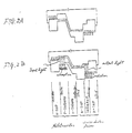
- Fig. 2A is an energy diagram illustrating the state of this preferred embodiment when a bias voltage is applied in the absence of optical input
- Fig. 2B is another energy diagram illustrating the state of the embodiment in the presence of an optical input, referring to light absorption, photocurrent and light emitting process at the same time.
- this structure requires only the laying of a semiconductor laser and a phototransistor over a semiconductor substrate, crystalline growth can be achieved by the conventional method, needing no more than one stage of crystalline growth unless the semiconductor laser is buried or two stages even if it is buried.
- the manufacturing procedure is simple because what is needed is, after electrode formation on one face following crystalline growth, merely to grind the other face to a desired thickness.
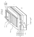
- Fig. 3 shows an oblique view of a second preferred embodiment of the present invention, wherein an electrode 115 for injecting electrons into a semiconductor laser 2 is newly formed in the axial direction of a resonator to reduce the load on its phototransistor.
- the phototransistor 3 is formed over approximately half the length of a mesa stripe 104 from an end face of the semiconductor laser 2; an n-InP layer 107 is subjected to Zn diffusion in a direction normal to that of the mesa stripe approximately in the middle of the mesa stripe to be converted into a p-type, and an electric separation layer (10 microns wide) 114 is formed as far as it reaches a second current blocking layer 106.
- a second n-electrode 115 is formed over an n-InP buried layer 107.
- the bottom of a substrate 100 includes the p-electrode 113.
- Fig. 4 shows an oblique view of a third preferred embodiment of the present invention, wherein another electrode is formed in a base layer 109 to control the current flowing through a phototransistor 3 with not only optical signals but also the current of the base layer 109.
- Crystalline growth and the formation of an n-electrode 112 and a light receiving face 111 of the phototransistor 3 are achieved in respectively the same manners as in the first preferred embodiment.
- This embodiment involves the phototransistor 3, whose light receiving face 111 and electrode 112 are formed, behind the mesa axis of a multilayered structure comprising a collector layer 108, a base layer 109 and an emitter layer 110, and an AuZn base electrode 116 formed over the base layer 109 before the mesa axis, where the emitter layer 110 is removed.
- the base electrode 116 since the base electrode 116 enables a base current to flow as well, it is possible to control the current flowing through the phototransistor 3 with not only optical signals but also the base current.
- the embodiments of the present invention can have many different versions.
- the dimensions of the light receiving face 111 of the phototransistor 3 are not particularly limited. Nor are the shape, dimensions and material of the n-electrode 112. Also acceptable is a combination of the second and third preferred embodiments, which has both a second n-electrode 115 for injecting electrons into the semiconductor laser 2 and a base electrode 116 for controlling the current in the phototransistor 3.
- the stripe of the semiconductor laser need not be buried, but can be structured in many other ways, for instance in a planar stripe form. In the foregoing embodiments, the n-type and p-type can be reversed. Although InP/InGaAsP-based semiconductor materials are used in these embodiments, other semiconductor materials, including GaAlAs/GaAs-based ones, can also be used.
Landscapes
- Physics & Mathematics (AREA)
- Condensed Matter Physics & Semiconductors (AREA)
- General Physics & Mathematics (AREA)
- Electromagnetism (AREA)
- Optics & Photonics (AREA)
- Geometry (AREA)
- Semiconductor Lasers (AREA)
- Light Receiving Elements (AREA)
- Solid State Image Pick-Up Elements (AREA)
- Photo Coupler, Interrupter, Optical-To-Optical Conversion Devices (AREA)
Applications Claiming Priority (2)
| Application Number | Priority Date | Filing Date | Title |
|---|---|---|---|
| JP59099122A JPH0682885B2 (ja) | 1984-05-17 | 1984-05-17 | 光増幅発光受光集積素子 |
| JP99122/84 | 1984-05-17 |
Publications (3)
| Publication Number | Publication Date |
|---|---|
| EP0164604A2 true EP0164604A2 (fr) | 1985-12-18 |
| EP0164604A3 EP0164604A3 (en) | 1987-08-19 |
| EP0164604B1 EP0164604B1 (fr) | 1991-08-07 |
Family
ID=14238965
Family Applications (1)
| Application Number | Title | Priority Date | Filing Date |
|---|---|---|---|
| EP85106017A Expired EP0164604B1 (fr) | 1984-05-17 | 1985-05-15 | Elément amplificateur intégré à émission et réception de lumière |
Country Status (4)
| Country | Link |
|---|---|
| US (1) | US4698821A (fr) |
| EP (1) | EP0164604B1 (fr) |
| JP (1) | JPH0682885B2 (fr) |
| DE (1) | DE3583702D1 (fr) |
Cited By (1)
| Publication number | Priority date | Publication date | Assignee | Title |
|---|---|---|---|---|
| EP0477086A1 (fr) * | 1990-09-21 | 1992-03-25 | Thomson-Csf | Convertisseur de fréquences lumineuses |
Families Citing this family (1)
| Publication number | Priority date | Publication date | Assignee | Title |
|---|---|---|---|---|
| JPS62194237A (ja) * | 1986-02-20 | 1987-08-26 | Kyohei Sakuta | 光増幅機能を有する3結合導波路光タツプ |
Family Cites Families (1)
| Publication number | Priority date | Publication date | Assignee | Title |
|---|---|---|---|---|
| US4349906A (en) * | 1979-09-18 | 1982-09-14 | Xerox Corporation | Optically controlled integrated current diode lasers |
-
1984
- 1984-05-17 JP JP59099122A patent/JPH0682885B2/ja not_active Expired - Lifetime
-
1985
- 1985-05-14 US US06/733,683 patent/US4698821A/en not_active Expired - Lifetime
- 1985-05-15 DE DE8585106017T patent/DE3583702D1/de not_active Expired - Lifetime
- 1985-05-15 EP EP85106017A patent/EP0164604B1/fr not_active Expired
Non-Patent Citations (2)
| Title |
|---|
| IEEE ELECTRON DEVICE LETTERS, vol. EDL-2, no. 4, April 1981, pages 99-100, New York, US; H. BENEKING "Full solid state image converter based on integration of phototransistors and LEDs" * |
| JAPANESE JOURNAL OF APPLIED PHYSICS. SUPPLEMENTS, vol. 22, supplement no. 22-1, 1983, pages 279, 282, Tokyo, JP; A. SASAKI et al.: "Monolithic integrated device for light amplification" * |
Cited By (3)
| Publication number | Priority date | Publication date | Assignee | Title |
|---|---|---|---|---|
| EP0477086A1 (fr) * | 1990-09-21 | 1992-03-25 | Thomson-Csf | Convertisseur de fréquences lumineuses |
| FR2667207A1 (fr) * | 1990-09-21 | 1992-03-27 | Thomson Csf | Convertisseur de frequences lumineuses. |
| US5247168A (en) * | 1990-09-21 | 1993-09-21 | Thomson-Csf | Light frequency converter having laser device connected in series with photodetector |
Also Published As
| Publication number | Publication date |
|---|---|
| JPH0682885B2 (ja) | 1994-10-19 |
| US4698821A (en) | 1987-10-06 |
| JPS60242688A (ja) | 1985-12-02 |
| EP0164604A3 (en) | 1987-08-19 |
| EP0164604B1 (fr) | 1991-08-07 |
| DE3583702D1 (de) | 1991-09-12 |
Similar Documents
| Publication | Publication Date | Title |
|---|---|---|
| US7199441B2 (en) | Optical module device driven by a single power supply | |
| US4742378A (en) | Junction-type semiconductor light emitting device with mesa | |
| Bar-Chaim et al. | GaAs integrated optoelectronics | |
| JPS6079788A (ja) | 光双安定素子 | |
| JPS6289391A (ja) | 集積型レ−ザ受光素子の製造方法 | |
| JP2980435B2 (ja) | 半導体装置 | |
| US4349906A (en) | Optically controlled integrated current diode lasers | |
| US5780880A (en) | High injection bipolar transistor | |
| JPH0738457B2 (ja) | 光・電子双安定素子 | |
| US5214663A (en) | Semiconductor laser | |
| US4698821A (en) | Integrated light emitting/receiving amplifier element | |
| US20040013146A1 (en) | Laser diode with a low absorption diode junction | |
| JPS63116489A (ja) | 光集積回路 | |
| US4779283A (en) | Semiconductor light emitting device | |
| JPH0312474B2 (fr) | ||
| JPS58207690A (ja) | 埋め込み形半導体レ−ザ | |
| JPH04144182A (ja) | 光半導体装置アレイ | |
| JP2000101186A (ja) | 半導体光素子およびその製造方法 | |
| JPS60239082A (ja) | 光増幅発光受光集積素子 | |
| JP2527197B2 (ja) | 光集積化素子 | |
| JPS60145690A (ja) | 光双安定発光受光集積素子 | |
| JPS5886789A (ja) | 半導体レ−ザ・フオトデイテクタ光集積化素子 | |
| JPS6119187A (ja) | 光集積回路素子 | |
| JPH067630B2 (ja) | 三端子半導体レ−ザ装置 | |
| JPH06101557B2 (ja) | 光集積回路 |
Legal Events
| Date | Code | Title | Description |
|---|---|---|---|
| PUAI | Public reference made under article 153(3) epc to a published international application that has entered the european phase |
Free format text: ORIGINAL CODE: 0009012 |
|
| 17P | Request for examination filed |
Effective date: 19850515 |
|
| AK | Designated contracting states |
Designated state(s): DE FR GB |
|
| PUAL | Search report despatched |
Free format text: ORIGINAL CODE: 0009013 |
|
| AK | Designated contracting states |
Kind code of ref document: A3 Designated state(s): DE FR GB |
|
| 17Q | First examination report despatched |
Effective date: 19880621 |
|
| GRAA | (expected) grant |
Free format text: ORIGINAL CODE: 0009210 |
|
| AK | Designated contracting states |
Kind code of ref document: B1 Designated state(s): DE FR GB |
|
| REF | Corresponds to: |
Ref document number: 3583702 Country of ref document: DE Date of ref document: 19910912 |
|
| ET | Fr: translation filed | ||
| PLBE | No opposition filed within time limit |
Free format text: ORIGINAL CODE: 0009261 |
|
| STAA | Information on the status of an ep patent application or granted ep patent |
Free format text: STATUS: NO OPPOSITION FILED WITHIN TIME LIMIT |
|
| 26N | No opposition filed | ||
| PGFP | Annual fee paid to national office [announced via postgrant information from national office to epo] |
Ref country code: GB Payment date: 19940511 Year of fee payment: 10 Ref country code: FR Payment date: 19940511 Year of fee payment: 10 |
|
| PGFP | Annual fee paid to national office [announced via postgrant information from national office to epo] |
Ref country code: DE Payment date: 19940729 Year of fee payment: 10 |
|
| PG25 | Lapsed in a contracting state [announced via postgrant information from national office to epo] |
Ref country code: GB Effective date: 19950515 |
|
| GBPC | Gb: european patent ceased through non-payment of renewal fee |
Effective date: 19950515 |
|
| PG25 | Lapsed in a contracting state [announced via postgrant information from national office to epo] |
Ref country code: DE Effective date: 19960201 |
|
| PG25 | Lapsed in a contracting state [announced via postgrant information from national office to epo] |
Ref country code: FR Effective date: 19960229 |
|
| REG | Reference to a national code |
Ref country code: FR Ref legal event code: ST |
|
| REG | Reference to a national code |
Ref country code: FR Ref legal event code: ST |